![[Search a list of Patent Appplications for class 438]](../as.gif) CLASS 438, CLASS 438, | SEMICONDUCTOR DEVICE MANUFACTURING: PROCESS |
| Click here for a printable version of this file | |
SECTION I - CLASS DEFINITION
A. This class provides for manufacturing a semiconductor containing a solid-state device by a combination of operations wherein:
(1) no other class provides for the overall combination, and
(2) the intent is to use the electrical properties of the semiconductor in the device for at least one of the following purposes: (a) conducting or modifying an electrical current, (b) storing electrical energy for subsequent discharge within a microelectronic integrated circuit, or (c) converting electromagnetic wave energy to electrical energy or electrical energy to electromagnetic energy.
B. This class provides for a species of Class 427 operations involving:
(1) coating a substrate with a semiconductive material, or
(2) coating a semiconductive substrate or substrate containing a semiconductive region;
wherein the intent is to use the electrical properties of the semiconductor in a solid-state device for at least one of the following purposes: (a) conducting or modifying an electrical current, (b) storing electrical energy for subsequent discharge within a microelectronic integrated circuit, or (c) converting electromagnetic wave energy to electrical energy or electrical energy to electromagnetic energy.
C. This class provides for a species of Class 216 operations involving etching a semiconductive substrate or etching a substrate containing a semiconductive region, wherein the intent is to use the electrical properties of the semiconductor in a solid-state device for at least one of the following purposes:
(1) conducting or modifying an electrical current,
(2) storing electrical energy for subsequent discharge within a microelectronic integrated circuit, or
(3) converting electromagnetic wave energy to electrical energy or electrical energy to electromagnetic energy.
D. This class provides for packaging (e.g., with mounting, encapsulating, etc.) or treatment of packaged semiconductor, when not elsewhere provided, wherein there are:
(1) multiple operations having a step of permanently attaching or securing a semiconductive substrate to a terminal, elongated conductor, or support (e.g., mounting, housing, lead frame, discrete heat sink, etc.),
(2) multiple operations having a step of shaping flowable plastic or flowable insulative material about a semiconductive substrate, or
(3) a step of treating an already packaged semiconductor substrate (e.g., coating, etching, etc.); if the following conditions are also met: (a) there is significant semiconductor chip structure (e.g., such as recited semiconductor junction, etc.) or named semiconductor device (e.g., DRAM, CMOS, EPROM, etc.), or (b) there is no significant semiconductor structure if also combined with a coating operation of this class (see B above) or etching operation of this class (see C above), and (c) the intent is to use the electrical properties of the semiconductor in a solid-state device for at least one of the following purposes: (i) conducting or modifying an electrical current, (ii) storing electrical energy for subsequent discharge within a microelectronic integrated circuit, or (iii) converting electromagnetic wave energy to electrical energy or electrical energy to electromagnetic energy;
| (1) Note. When Class 438 coating (see B above) or etching operations (see C above) are not included, Class 29, following historical precedence, provides for processes of mounting, packaging, molding, or encapsulating of semiconductors having no significant semiconductor chip structure (e.g., merely recited as semiconductor chip, per se, etc.) when not elsewhere provided. E. This is the generic class for operations not elsewhere provided for treating a semiconductive substrate or substrate containing a semiconductive region; wherein the intent is to use the semiconductor in a solid-state device for at least one of the following purposes: (1) conducting or modifying an electrical current, (2) storing electrical energy for subsequent discharge within a microelectronic integrated circuit, or (3) converting electromagnetic wave energy to electrical energy or electrical energy to electromagnetic energy. |
| (1) Note. Lacking an indication that the semiconducting material is to be used for a purpose other than (a) conducting or modifying an electrical current, (b) storing electrical energy for subsequent discharge within a microelectronic integrated circuit, or (c) converting electromagnetic wave energy to electrical energy or electrical energy to electromagnetic energy; it will be assumed that the process meets the Class 438 definition. |
| (2) Note. For this class certain materials will be considered to be semiconductors even if there is no other indication that semiconducting properties are present. Thus, if the criteria set forth under the (1) Note is met that there is no indication that the material is to be used for a purpose other than (a), (b), or (c), the following materials are to be considered semiconductive: silicon, germanium, selenium, tellurium, gallium nitride, gallium phosphide, gallium arsenide, aluminum phosphide, aluminum arsenide, and mercury cadmium telluride. |
SECTION II - LINES WITH OTHER CLASSES AND WITHIN THIS CLASS
Several classes provide for plural step operations for manufacturing semiconductor solid-state devices or components therefor. Combined operations for manufacturing semiconductor electrical devices or semiconductor-based components therefor having plural steps not encompassed by another class are proper for Class 438.
For example, while plural steps acceptable to Class 264 (e.g., injection molding and subsequent removal of flash, etc.) remain in Class 264, combinations of molding and adhesive bonding are provided for in Class 156, even though this involves multiple steps, one of which (i.e., molding) would be considered a Class 264 unit operation even if semiconductor material is involved. However, combinations of molding, adhesive bonding, and a Class 438 unit operation acting on a semiconductor substrate which is used for at least one of the following purposes: (a) conducting or modifying an electrical current, (b) storing electrical energy for subsequent discharge within a microelectronic integrated circuit, or (c) converting electromagnetic wave energy to electrical energy or electrical energy to electromagnetic energy, are considered proper for Class 438.
A. UNIT COATING OPERATIONS, COMBINED OPERATIONS INVOLVING COATING, AND PARTICLE BOMBARDMENT
The following search notes are intended to clarify the lines and distinctions for determining when coating operations are provided for in Class 438. Throughout this class, the term "coating" is used in the generic sense to include both surface coating and impregnation.
The unit coating operations in Class 438 may be viewed as a specie of a Class 427 process which was removed intact from Class 427 and transferred to Class 438 for the convenience of the searcher. Thus, plural step operations that were acceptable in Class 427 are now acceptable in Class 438 if the criteria for the semiconductor material as set forth hereinabove is met. Coating operations which do not meet the Class 438 definition may be classified in the classes identified in References to Other Classes, below.
B. UNIT ETCHING OPERATIONS AND COMBINED ETCHING OPERATIONS IN CLASS 438
In References to Other Classes, below, are search notes are intended to clarify the lines and distinctions for determining when an etching unit operation is provided for in Class 438. Throughout this class, the term "etching" is used in the generic sense to include the removal of a surface by chemical reaction or solvent action regardless of the composition thereof.
The unit etching operations in Class 438 may be viewed as a specie of a Class 216 process which was removed intact from Class 216 and transferred to Class 438 for the convenience of the searcher. Thus, plural step operations that were acceptable in Class 216 are now acceptable in Class 438 if the criteria for the semiconductor material as set forth hereinabove is met. Etching operations which do not meet the Class 438 definition may be found in References with Other Classes, below.
C. PACKAGING (E.G., WITH MOUNTING, ENCAPSULATING, ETC.) OR TREATMENT OF PACKAGED SEMICONDUCTOR
Packaging is a semiconductor art manufacturing term for integration, assembly, or surrounding of a semiconductive substrate (e.g., chip, die, etc.) with a permanent encasement, housing, capsule, or support. This is distinguished from package making found in Class 53 which is directed to preparing a manufactured product for passage through the channels of trade in a safe, convenient, and attractive condition, usually wrapped in a cover or in a container which is intended to be removed when the manufactured product is used.
Class 438 takes the following packaging or packaging related operations, if not elsewhere provided: (a) multiple operations having a step of permanently attaching or securing a semiconductive substrate to a terminal, elongated conductor, or support (e.g., mounting, housing, lead frame, discrete heat sink, etc.), (b) multiple operations having a step of shaping flowable plastic or flowable insulative material about a semiconductive substrate, or (c) a step of treating an already packaged semiconductor substrate (e.g., coating, etching, etc.).
However, other manufacturing classes have established historic lines with Class 438 that must be considered when determining proper placement. These lines with external classes revolve around such concepts as: whether there is significant semiconductor device structure, whether there is a unit operation or a so-called "multi-step" operation, etc. The search notes in References to Other Classes, below, are intended to clarify these established lines and to alert the searcher to other classes for related searches.
D. LINE NOTES TO OTHER MANUFACTURING OPERATIONS
See References to Other Classes, below for lines clarifying the relationship of other chemical classes to Class 438. For many of the chemical classes, inclusion of metal casting, working or deforming, or fusion bonding step is not acceptable if combined with an operation of the chemical class.
E. LOCATION OF SEMICONDUCTOR COMPOUND, COMPOSITION, OR STOCK
Class 438 does not provide for compound, composition, or stock material produced or utilized by a Class 438 process. A process of manufacture or use of a compound or composition is usually classified with the compound or composition. The process of manufacturing a semiconductor compound or composition and the formation of a semiconductor device or semiconductor junction takes combined operations to Class 438.
Also see References to Other Classes, below, identifying this section.
F. LINE TO HEATING CLASSES
This class (438), will take the process of (a) heating of semiconductor material to modify the microstructure or electrical properties thereof, (b) combined operations involving heating of semiconductor material to modify the semiconductor structure or electrical properties when not provided in another class, or (c) heating of semiconductor substrates that affects only the nonsemiconductor region of the substrate when combined with other operations acceptable to Class 438 or combined with the establishment of device structure (e.g., connects, insulating regions, electrodes, etc.).
See References to Other Classes, below, identified as heating classes.
G. LINE NOTES TO ELECTRICAL CLASSES
See References to Other Classes, below.
SECTION III - REFERENCES TO OTHER CLASSES
SEE OR SEARCH CLASS:
| 29, | Metal Working, especially
subclasses 729+ for electrical device manufacturing apparatus, subclasses
829+ for the assembly of electrical components to an insulative
base having a conductive path applied thereto, or formed
thereon or therein (e.g., a
printed circuit board). [See "Packaging (e.g., With
Mounting, Encapsulating, etc.)" above]
| ||||||
| 53, | Package Making, for passage through the channels of trade in a
safe, convenient, and attractive condition, usually
wrapped in a cover or in a container. In this context
of trade, Class 53 provides for methods of: (a) encompassing, encasing, or
completely surrounding goods or materials with a cover made from
sheet stock, (b) partially encasing or
surrounding goods and materials by a partial cover made from sheet stock, (c) assembling
or securing a separate closure to an aperture of a preformed receptacle
to complete encasement of contents, (d) depositing
articles and arranging fluent materials in preformed receptacles, (e) partial
or complete shaping of a cover about an article, and other
related package making processes. (See "Packaging (E.g., With
Mounting, Encapsulating, Etc.)" above)
| ||||||
| 65, | Glass Manufacturing, for processes of melting, shaping or forming, joining, or
heat treating of glass. Glass is defined in the Class
65 definitions (Glossary) as an inorganic material generally
including a glass former and having specific characteristics provided
in the definition. Included in Class 65 is joining, per
se, of glass to metal or glass. (See "Packaging (e.g., With
Mounting, Encapsulating, etc.)" above)
| ||||||
| 65, | Glass Manufacturing, for processes of melting, shaping or forming, joining, or
heat treating of glass. Glass is defined in the Class
65 definitions (Glossary) as an inorganic material generally
including a glass former and having specific characteristics provided
in the definition. It is noted that both silica and elemental silicon
are also included for Class 65. Thus, melting, shaping, or
fusion bonding of silicon dioxide, per se, or
silicon, per se, is also considered proper for
Class 65. Class 65 also takes combined operations whether
preparatory or subsequent to the melting, shaping or forming, joining
or heat treating of glass. Included in Class 65 is joining, per
se, of glass to metal, spinning, per
se, of glass fibers or joining through glass melting, per
se, of glass fibers to substrates such as semiconductor
substrates. (see "Line Notes To Other
Manufacturing Operations," above)
| ||||||
| 106, | Compositions: Coating or Plastic, subclasses 1.05+ for metal-deposition or substrate-sensitizing compositions; subclasses 286.1+ for inorganic materials only containing at least one metal atom; subclass 286.8 for inorganic materials only; subclasses 287.1+ for silicon containing other than solely as silicon dioxide as a part of an aluminum-containing compound, and subclasses 400+ for materials or ingredients. (see "Location Of Semiconductor Compound, Composition, Or Stock" above.) | ||||||
| 117, | Single-Crystal, Oriented-Crystal, and
Epitaxy Growth Processes; Non-Coating Apparatus Therefore, for processes of single crystal growth of semiconductor
material upon a seed or substrate and perfecting operations combined
therewith. See Class 117 definitions for examples of perfecting
operations generally acceptable to Class 117. See particularly
Class 117, Class Definition, (2) Note, Keywords
and (3) Note, Indicative Terminology, for
terms indicative of single crystal formation. Inclusion
of a nonperfecting single crystal forming operation on a semiconductor
substrate or producing a semiconductor product meeting the hereinabove
requirements of a semiconductor material or the definition of a
semiconductor substrate takes the original to Class 438, even if
there is present a single crystal forming step. (Coating
operation not meeting Class 438 definition)
| ||||||
| 134, | Cleaning and Liquid Contact With Solids, especially
subclass 1.2 and 1.3 for processes for cleaning a semiconductor
substrate including the application of electrical or wave energy to
the substrate. (Etching operation not meeting the
Class 438 definition)
| ||||||
| 148, | Metal Treatment, for unit coating operations on metal, particularly
subclasses 206+ wherein there is carburization or nitriding of
a metal surface by chemical reaction or diffusion of an externally
supplied source of carbon or nitrogen that reacts with the metal
surface wherein the metal substrate remains as part of the coating
and subclasses 240+wherein there
is reactive coating of a metal substrate with an external reactant (e.g., oxygen, etc.) wherein the
metal substrate remains as part of the coating. Class 148
also takes heat treatment of metallic compositions if during the
heat treatment there is either a change in the internal physical
structure (i.e., microstructure) or chemical
properties. (Coating operation not meeting Class
438 definition)
| ||||||
| 148, | Metal Treatment, subclasses 33.1+ for semiconductor stock which must be essentially homogeneous and have at least two contiguous layers differing in the number of unbound electrons and/or differing in energy gap levels, which exhibit a junction between the layers. (see "Location of Semiconductor Compound, Composition, or Stock" above.) | ||||||
| 148, | Metal Treatment, for processes of heat treating metals. Class 148 takes heat treatment of metallic compositions if during the heat treatment there is either a change in the internal physical structure (i.e., microstructure) or chemical properties. Since in certain instances metallic compositions could be semiconductor material meeting the Class 438 criteria, placement will go to Class 438 over Class 148 if the material is identified or perceived as semiconductor material. If perceived, a mandatory cross is made in Class 148. (heating class) | ||||||
| 156, | Adhesive Bonding and Miscellaneous Chemical Manufacture, subclasses 60 through 338for processes of adhesively bonding and subclasses 701-719 and 930-932 for processes of delaminating, per se, while retaining identity as semiconductive. Multistep processes for packaging semiconductors having no significant semiconductor chip structure are proper for Class 156 when claiming (a) adhesive bonding combined with shaping of nonmetals, (b) adhesive bonding combined with broad or nominally claimed metal-shaping steps, or (c) adhesive bonding including steps for assembling the parts to be bonded. An adhesive bonding unit operation for packaging or mounting operations on semiconductor devices goes as original to Class 156. Adhesive bonding combined with Class 438 coating of a semiconductor substrate or Class 438 etching of a semiconductor substrate places the original in Class 438. (See Packaging (e.g., With Mounting, Encapsulating, etc.) above). | ||||||
| 174, | Electricity: Conductors and Insulators, subclasses 15.1 through 16.3for fluid cooling of electrical conductors or insulator, subclasses 50-64 for housings with electric devices or mounting means, and subclasses 250-268 for printed circuit devices. | ||||||
| 204, | Chemistry: Electrical and Wave Energy, particularly
subclasses 192.1 through 192.37for sputter coating operations involving semiconductor
material or substrates including a semiconductor region, even
if the intent is to use the semiconductor material for (a) conducting
or modifying an electrical current, (b) storing electrical
energy for subsequent discharge within a microelectronic integrated
circuit, or (c) converting electromagnetic
wave energy to electrical energy or electrical energy to electromagnetic
energy - Class 204 will take combinations of sputter coating
with other chemical treating operations that involve (a) preparatory treatment
of the substrate (e.g., etching, cleaning, etc.) or (b) subsequent
perfecting treatment of the applied coating with the following exception
noted (coating operation not meeting Class 438 definition); and
subclasses 192.32-192.37, for
sputter etching operations on semiconductor material and semiconductor
containing substrates, even if the semiconductor is intended
for electrical purposes - simultaneous sputter etching
and chemical etching (e.g., as when
utilizing a mixture of argon and halide gas, etc.) go
as original in Class 204 (etching operation not meeting
the Class 438 definition).
| ||||||
| 205, | Electrolysis: Processes, Compositions Used Therein, and Methods of Preparing the Compositions, particularly subclass 123 , 124, and 157 for electrolytic coating operations on semiconductor or semiconductor devices (coating operation not meeting Class 438 definition), subclasses 334-639 for electrolytic synthesis of material, such as silicon, by passing an electrical current through a fused material, and subclass 656 for electrolytic erosion of a workpiece of non-uniform internal electrical characteristics (etching operation not meeting the Class 438 definition). Class 205 will take combinations of electrolytic coating with other chemical treating operations that involve (a) preparatory treatment of the substrate (e.g., etching, cleaning, etc.) or (b) subsequent perfecting treatment of the applied coating with the following exception noted (coating operation not meeting Class 438 definition). | ||||||
| 216, | Etching a Substrate: Processes, for chemical etching processes and perfecting operations therefor, including
lithos:graphic steps, of semiconductor material
that is to be utilized for nonelectrical properties. (Etching
operation not meeting the Class 438 definition)
| ||||||
| 219, | Electric Heating, subclasses 78.01+ for a process and apparatus for bonding by electrical current and pressure, and appropriate subclasses for electric heating of material, per se. However, inclusion of the criteria for Class 438 as set forth hereinabove takes the original to Class 438 even when electric heating is involved. (heating class) | ||||||
| 228, | Metal Fusion Bonding, appropriate subclasses for a process of fusion bonding and additional operations which are considered to be ancillary to the bonding (preheating, positioning, pretinning, etc.) of a semiconductive substrate; especially note subclass 123.1 and 179.1+. [See "Packaging (e.g., With Mounting, Encapsulating, etc.)" above] | ||||||
| 250, | Radiant energy, for methods not elsewhere provided of (a) using, generating, controlling, or detecting radiant energy, (b) combinations including such methods, and (c) subcombinations thereof. Particularly, see subclasses 492.2+ for processes of irradiation of semiconductor devices with no indication as to what occurs to the substrate. Class 250, subclasses 492.2+, generally relates to processes of exposing substrates to ion bombardment utilizing apparatus of Class 250 when limited to operating the apparatus in apparatus terms. Class 250 is also the generic home for processes of exposing substrates to ion bombardment. However, Class 438 provides for ion implantation of semiconductive substrate or substrate containing a semiconductive region and also ion implantation throughout the material mass to produce semiconductive material or to modify the semiconductive material. (Coating operation not meeting Class 438 definition) | ||||||
| 250, | Radiant Energy, for methods not elsewhere provided, of (a) using, generating, controlling, or detecting radiant energy, (b) combinations including such methods, and (c) subcombinations thereof. Particularly, see subclasses 492.2+ for processes of irradiation of semiconductor devices with no indication as to what occurs to the substrate. Class 250 subclasses 492.2+, generally relates to processes of exposing substrates to ion bombardment utilizing apparatus of Class 250 when limited to operating the apparatus in apparatus terms. Class 250 is also the generic home for processes of exposing substrates to ion bombardment. However, Class 438 takes chemically reactive ion etching of semiconductive substrate or substrate containing semiconductive region. (Etching operation not meeting the Class 438 definition) | ||||||
| 250, | Radiant Energy, for heating invisible radiant energy; subject matter of Class 438, per se, when no function other than heating is attributed to the process and for methods not elsewhere provided, of (a) using, generating, controlling, or detecting radiant energy, (b) combinations including such methods, and (c) subcombinations thereof. Particularly, see subclasses 492.2+ for processes of ion bombardment or irradiation of semiconductor devices, with no indication as to what occurs to the substrate. (heating class) | ||||||
| 252, | Compositions, for (a) subclasses 62.3+ for semiconductor compositions which have been uniformly doped or otherwise specialized for use as one layer which when combined with another such layer would provide an interface exhibiting barrier layer properties (e.g., as exists in Class 148, subclasses 33 through 33.6, stock wherein there is a semiconductor junction, etc.) and (b) subclasses 500+ for electrical conductive compositions. Also see the cross-reference art collection in Class 252, subclasses 950+, for doping agent source materials. (see "Location Of Semiconductor Compound, Composition, Or Stock" above.) | ||||||
| 257, | Active Solid-State Devices (e.g., Transistors, Solid-State Diodes), for active solid-state electronic device structure, per se. Subject matter may include one or more such devices combined with contacts or leads, or structures configured to be tested on a semiconductor chip, or merely semiconductor material without contacts or leads where the sole disclosed use is an active solid-state device. This subject matter does not include active solid-state devices combined with significant circuits. (electrical class) | ||||||
| 264, | Plastic and Nonmetallic Article Shaping or Treating: Processes, for a process (and steps perfecting same) of forming a composite by shaping a plastic or nonmetallic wherein a semiconducting containing preform is within a mold during the shaping operation (e.g., encapsulating, etc.). (See "Packaging (e.g., With Mounting, Encapsulating, etc.)" above) | ||||||
| 361, | Electricity: Electrical Systems and Devices, subclasses 679.01 through 679.61for housing and mounting assemblies for electronic devices and components, and subclasses 736+ and 752+ for modules for printed circuits or housing or chassis for printed circuit boards. (electrical class). | ||||||
| 376, | Induced Nuclear Reactions: Processes, Systems, and Elements, particularly subclass 183 for a process of neutron bombardment, per se, of semiconductive material containing an element which is converted to a desired dopant by nuclear transmutation. Any combination of operations that goes beyond formation of the transmutated doped semiconductor material, per se, goes as original to Class 438 if it meets the criteria of the intent to use the electrical properties of the semiconductor in a solid-state device as set forth by the Class 438 definition. (Coating operation not meeting Class 438 definition) | ||||||
| 376, | Induced Nuclear Reactions: Processes, Systems, and Elements, subclasses 320+ for the direct conversion of the energy produced in a nuclear reaction into an electrical output by a one-step process or apparatus for accomplishing such a one-step process. (electrical class) | ||||||
| 378, | X-ray or Gamma Ray Systems or Devices, especially subclasses 34+ for X-ray or gamma-ray lithography. (electrical class) | ||||||
| 382, | Image Analysis, especially subclass 145 for a process limited to image analysis per se in manufacturing of an integrated circuit. However, inclusion of subject matter for Class 438 remains with Class 438 even if there is a step of image analysis. | ||||||
| 385, | Optical Waveguides, particularly, subclass 14 for a laser in integrated optical circuit, subclasses 129+ for a planar optical waveguide, and subclasses 141+ for a waveguide having a particular optical characteristic modifying chemical composition. The (13) Note of Class 385 indicates that miscellaneous manufacturing of optical wave guide devices not elsewhere provided are in Class 385. Thus, if the manufactured article is a semiconductor device, a Class 438 process controls over the Class 385 process even if an optical fiber is part of the device. (electrical class) | ||||||
| 420, | Alloys or Metallic Composition, for alloys or metallic compositions that may also exhibit semiconductor properties (e.g., gallium arsenide, etc.). (see "Location Of Semiconductor Compound, Composition, Or Stock" above.) | ||||||
| 423, | Chemistry of Inorganic Compounds, appropriate subclasses for inorganic compounds or elements used in the manufacture of semiconductor devices. (see "Location of Semiconductor Compound, Composition, or Stock" above.) | ||||||
| 427, | Coating Processes, for coating operations provided for in that class, particularly
subclasses 457+ for a process of treating a coating with radiant
energy; subclasses 487+ for polymerization of
applied coating utilizing direct application of electrical, magnetic, wave, or particulate
energy; subclasses 523+ for ion plating or ion
implanting; subclasses 532+ for pretreatment of
a substrate or posttreatment of a coated substrate utilizing electrical, magnetic, wave, or
particulate energy; subclasses 569+ for deposition
coating processes utilizing plasma; subclasses 580+ for
deposition coating processes utilizing electrical discharge; subclass
581 for coating processes utilizing chemical liquid deposition; subclass
582 for coating processes utilizing photo-initiated chemical vapor
deposition; subclasses 585+ for coating processes
utilizing chemical vapor deposition; subclass 591 for deposition
coating utilizing induction or dielectric heating; subclasses
592+ for deposition coating utilizing resistance heating; subclasses
595+ for deposition coating utilizing electromagnetic or
particulate radiation; subclasses 598+ for deposition
coating utilizing magnetic field or force; subclass 600
for deposition coating utilizing sonic or ultrasonic energy. (Coating
operation not meeting Class 438 definition)
| ||||||
| 428, | Stock Material or Miscellaneous Articles, appropriate subclasses for semiconductor stock material defined in terms of composition and structure, especially subclass 620 . (see "Location of Semiconductor Compound, Composition, or Stock" above.) | ||||||
| 429, | Chemistry: Electrical Current Producing Apparatus, Product, and Process, especially subclass 7 for a combination including a nonbattery electrical component electrically connected within a cell casing other than testing or indicating components. (electrical class) | ||||||
| 430, | Radiation Imagery Chemistry: Process, Composition, or
Product Thereof, particularly for initial lithos:graphic
processes in semiconductor manufacture limited to (a) exposure
imaging and developing and including preparatory operations to the
exposure (e.g., as coating to form
the resist, etc.) or (b) developing, per
se, of subject matter of Class 430 substrates. When Class
430 exposure, imaging or developing are combined with etching
or coating of a semiconductor substrate for purposes other than masking
and commensurate with the Class 438 definition for manufacture of
a semiconductor device as set forth hereinabove, the combination
goes as original to Class 438 with the following exception noted.
(Coating operation not meeting Class 438 definition)
| ||||||
| 430, | Radiation Imagery Chemistry: Process, Composition, or
Product Thereof, particularly for initial lithos:graphic
processes in semiconductor manufacture limited to (a) exposure
imaging and developing and including preparatory operations to the
exposure (e.g., as coating to form
the resist, etc.) or (b) developing, per
se, of subject matter of Class 430 substrates. When Class
430 exposure imaging or developing are combined with etching or
coating of a semiconductor substrate commensurate with the Class
438 definition for manufacture of a semiconductor device as set
forth hereinabove, the combination goes as original to
Class 438 with the following exception noted. (Etching
operation not meeting the Class 438 definition)
| ||||||
| 432, | Heating, for generic heating processes. However, inclusion of the criteria for Class 438 as set forth hereinabove takes the original to Class 438 even when generic heating is involved. (heating class) | ||||||
| 439, | Electrical Connectors, appropriate subclasses for features related or analogous to electrical contact or housing features of active solid-state devices (e.g., subclasses 271+ for sealing elements or subclasses 449+ for stress relief means for conductor to terminal joint. (electrical class) | ||||||
| 501, | Compositions: Ceramic, appropriate subclasses for ceramic compositions used in semiconductor devices. (see "Location of Semiconductor Compound, Composition, or Stock" above.) | ||||||
| 505, | Superconductor Technology: Apparatus, Material, Process, particularly subclass 330 for processes of manufacturing from high temperature (i.e., above 30 degrees Kelvin) superconductive material (a) superconductor devices or (b) semiconductor devices having superconductive components or connect lines. (see "Line Notes To Other Manufacturing Operations," above) |
SECTION IV - GLOSSARY
Listed below are: (1) a compilation of acronyms, abbreviations, and technological terms pertaining to solid-state electrical devices, manufacturing processes, and related apparatus and compositions useful therefor and (2) the meaning to be given to the various "art" terms appearing in this class. These latter terms, some of which have been included in the glossary below, are the same as that generally accepted or in common usage. However, certain terms employed in this class and also included below have been assigned definitions which may be more restrictive or different from those in common usage since these terms are being utilized for distinguishing this class over other classes of related art.
a-Si
Amorphous silicon
ACT
Acoustic charge transport
ADC
Analog-to-digital converter
AES
Auger electron spectroscopy
ALE
Atomic layer epitaxy
ALEP
Angle-lapping edge profilometry
AMD
Active matrix display
AMG
Alternative-metal, virtual-ground (metallization)
APCVD
Atmospheric-pressure CVD
APD
Avalanche photodiode
ARC
antireflective coating
ASG
Arsenosilicate glass
BBCO
Barium bismuth copper oxide (a HTSC)
BBD
Bucket brigade device
BBL
Buried bit-line
BED
Band edge discontinuity
BH
Buried heterostructure
BHF
Buffered hydrofluoric acid
BIC
Breakdown of insulator for conduction
BICFET
Bipolar inversion channel FET
BiCMOS
Integrated bipolar and CMOS
BiMOS
Integrated bipolar and MOSFET
BJT
Bipolar junction transistor
BKBO
Barium potassium bismuth oxide (a HTSC)
BLM
Ball limiting metallization
BMD
Bulk micro defect
BOE
Buffered oxide etch
BOX
Buried oxide
BOXES
Buried oxide with etch stop
BPSG
Borophosphosilica glass
BPTEOS
borophosphoTEOS
BSD
Back side damage
BSE
buried storage electrode
BSG
Borosilica glass
BSQ
Bias sputter quartz
BST
Barium strontium titanate
CAIBE
Chemically assisted ion beam etching
CBIC
Complementary bipolar IC
CBKR
Cross bridge Kelvin resistor (test structure)
CCB
Controlled collapse bonding
CCC
Corrugated capacitor cell
CCD
Charge coupled device
CDE
Chemical dry etching
CDI
Collector diffusion isolation
CEL
Contrast enhancement layer
CER
Contact end resistor (test structure)
CERDIP
ceramic DIP
chanstop
channel stop isolation structure
CHEMFET
Chemically sensitive FET
CHL
Current hugging logic
CID
Charge injection device
CLSEG
Confined lateral SEG
CML
Current mode logic (i.e., ECL)
CMOS
Complementary (NMOS and PMOS) FETs
CMP
chemical-mechanical polishing/planarization
COB
(a) chip-on-board or (b) capacitor over bit-line
COD
Catastrophic optical damage
COG
Chip-on-glass
COMFET
Conductivity modulation FET (i.e., IGBT)
CSBH
Channeled substrate buried heterostructure
CSL
Coherent superlattice
CTD
Charge transfer device
CTSL
Coherent tilted superlattice
CVD
Chemical vapor deposition
Cz
Czoshralski (melt pulling)
DADBS
diacetoxyditertiarybutoxysilane
DADIS
diacetoxydiisopropoxysilane
DBR
distributed Bragg reflector
DCG
dichromated gelatin
DCFL
direct-coupled FET logic
DCS
dichlorosilane
DDE
double diffused epitaxy
DDI
deep dielectric isolation
DEIS
dual electron injection structure
DEZ
diethylzinc
DFB
distributed feedback (laser)
DH
double-hetero
DHBT
double-hetero bipolar transistor
DHF
dilute hydrofluoric acid
DI
dielectric isolation
DIBL
drain induced barrier lowering
DIET
dielectrically encapsulated trench capacitor
DIP
dual-in-line package
DLP
double layer polysilicon
DLTS
deep level transient spectroscopy
DMAH
dimethylaluminumhydride
DMD
(a) depletion mode device (also D-mode or D-type) or (b) deformable mirror device
DMOS
double diffused MOS
DMS
dilute magnetic semiconductor
DOES
doublehetero optoelectronic switch
DRAM
dynamic random-access memory
DSP
double stacked capacitor
DTL
diode-transistor logic
DUF
diffusion under film
DUT
device under test
DUV
deep ultraviolet
DZ
denuded zone
-E-
EAROM
electrically alterable read-only memory
EB
(a) extrinsic base or (b) electron beam
EBES
electron beam exposure system
EBIC
electron beam induced current
EBL
electron beam lithography
ECL
emitter coupled logic
ECR
electron cyclotron resonance
EDP
ethylene-diamine-pyrocatechol etchant
EDTA
ethylenediaminotetraacetic acid
EELS
electron energy loss spectroscopy
EEPROM
electrically erasable programmable read-only memory
EFG
edge-defined film-fed growth (also EDFFG or EDFG)
EG
extrinsic gettering
EGSi
electronic-grade silicon
EL
electroluminescent
ELO
epitaxial lateral overgrowth
EMD
enhancement mode device (also E-mode or E-type)
EMI
electromagnetic interference
EMP
electron microprobe
EPB
epoxidated polybutadiene (an EB resist)
EPD
etch pit density
EPI
epitaxial (single crystalline) layer
EPP
ethylene-piperidine-pyrocatechol etchant
EPR
electron paramagnetic resonance
EPROM
erasable programmable read-only memory
EPS
effective punchthrough stopper
EPW
etchant mix of ethylenediamine, pyrocatechol, and water
ESCA
electron spectroscopy for chemical analysis
ESD
electrostatic discharge
ESR
(a) equivalent series resistance or (b) electron spin resonance
FAMOS
floating-gate avalanche-injection MOS
FASIC
folded bit-line adaptive sidewall isol. capacitor cell
FCT
field controlled thyristor
FEC
floating electrode capacitor
FED
field emission device
FET
field effect transistor
FIB
focused ion beam
FIPOS
full isolation by porous oxidized silicon
FLOTOX
floating gate tunnel oxide
FOX
field oxide
FPD
field programmable device
FPGA
field programmable gate array
FTIR
Fourier transform infrared spectroscopy
FUROX
fully recessed oxide isolation
GDMS
glow discharge mass spectroscopy
GILD
gas immersion laser doping
GRIN-SCH
graded index separate confinement heterostructure
GTO
gate turn-off
HBT
heterojunction bipolar transistor
HDC
high dielectric constant
HDI
high density interconnects
HDMI
high density multilayer interconnects
HEMT
high electron mobility transistor (Hetero MESFET)
HET
hot electron transistor (bipolar)
Hi-C
high capacitance
HIC
hybrid integrated circuit
HIMOS
(see COMFET)
HIPOX
high pressure oxidation
HMDS
hexamethyldisilizane
HNA
hetchant mix of hydrofluoric, nitric, and acetic acids
HPSC
half-Vccsheath plate capacitor
HTO
high temperature oxide
HTSC
high temperature superconductor
IB
(a) intrinsic base or (b) ion beam
IBD
ion beam deposition
IC
integrated circuit
ICP
inductively coupled plasma
IG
intrinsic gettering
IGBT
insulated gate bipolar transistor (e.g., COMFET, HIMOS)
IGFET
insulated gate field effect transistor
IID
impurity induced disordering
I2L
integrated injection logic
IJP
ink jet printhead
ILB
inner lead bonding
ILD
interlayer dielectric
IMMA
ion microprobe mass analysis
IMPATT
impact ionization avalanche transist time (diode)
INS
intrinsic nondoped semiconductor
IR
infrared
ISFET
ion sensitive FET (i.e., CHEMFET)
ITO
indium tin oxide (a TCO)
IVEC
isolation vertical capacitor cell
JFET
junction field effect transistor (junction gate)
JOFET
Josephson junction field effect transistor
JTE
junction termination extension
KMER
Kodak metal etch resist
KPR
Kodak photo resist
KTFR
Kodak thin film resist
LAGB
low-angle grain boundary
LATID
large angle tilt implant drain
LB
(a) Langmuir-Blodgett or (b) laser beam
LCCD
leadless ceramic chip carrier
LCD
liquid crystal display
LDCC
leaded ceramic chip carrier
LDD
lightly doped drain
LEC
liquid encapsulated Czoshralski
LED
light emitting diode
LEED
low-energy electron diffraction
LEK
liquid encapsulated Kyropoulus
LOCOS
local oxidation of silicon
LOPED
lift-off using edge detection
LPCVD
low-pressure chemical vapor deposition
LPE
liquid phase epitaxy
LRP
limited reaction processing
LSI
large scale integration
LSSL
lateral surface superlattice
LST
logic service terminal
LTCC
low temperature co-fired ceramic
LTG
low temperature growth
LTO
low temperature oxidation
MBE
molecular beam epitaxy
MCz
magnetic Czoshralski
MCM
multichip module
MCT
(a) MOS controlled thyristor or (b) HgCdTe
MEM
micro-electromechanical
MESFET
metal semiconductor FET (Schottky gate)
MF3R
modified fully-framed fully-recessed isolation
MGSi
metallurgical-grade silicon
MIM
metal-insulator-metal
MISFET
metal insulator semiconductor IGFET
MLEC
magnetic LEC
MLC
multilayer ceramic
MLO
multilayer oxide
MLR
multilayer resist
MMA
methyl methacrylate
MMIC
monolithic microwave integrated circuit
MNOS
metal nitride/oxide IGFET
MOCVD
metal organic chemical vapor deposition
MODFET
modulation doped MESFET (i.e., HEMT)
MOMOM
metal-oxide-metal (tunnelling device)
MOSFET
metal oxide semiconductor IGFET
MQW
multiquantum well
MTF
mean time to failure
MTL
merged transistor logic (i.e., I2L)
NDC
negative differential conductivity
NEA
negative electron affinity (e-emitter)
NMA
N-methyl-acetamide
NMOS
n-channel MOSFET
NMP
n-methyl-pyrrolidone
novolak
Thermoplastic phenol-formaldehyde used as photoresist
NPN
(bipolar transistor)
NRD
nitridation retarded diffusion
NSAG
nonself-aligned gate
NTD
neutron transmutation doping
NVRAM
nonvolatile RAM
OBG
optical band gap
ODE
orientation dependent etching
OED
oxidation enhanced diffusion
OEIC
optoelectronic integrated circuit
OF
orientation flat
OISF
oxidation induced stacking fault
OMCVD
organometallic CVD
OMCT
octamethylcyclotetrasiloxane
OMVPE
organometallic VPE
ORD
oxidation retarded diffusion
ORL
optical return loss
OSA
optical subassembly
OSF
(see OISF)
OTCR
over-the-cell routing
OTP
one-time programmable
OXSEF
oxygen-doped silicon epitaxial film
PAC
photoactive compound
PAP
peel apart
PBG
photonic band gap
PBL
polybuffered LOCOS
PBM
planarization blocking mask
PBN
pyrolytic boron nitride
PBT
permeable base transistor
PCB
printed circuit board
PCE
photoconductive element
PEB
postexposure baking
PECVD
plasma enhanced chemical vapor deposition
PEP
photo-engraving process
PFT
peeled film technology
PGA
(a) pin-grid array or (b) programmable gate array
PGMA
poly(glycidyl methacrylate) (an EB resist)
PHS
plated heat sink
PIC
photonic integrated circuit
PID
programmable interconnect device (fuse/antifuse)
PIN
P-type layer, intrinsic layer, N-type layer
PIQ
thermosetting polyimide resin
PLA
programmable logic array
PLCC
plastic leaded chip carrier
PLDD
profiled LDD
PLM
pad limiting metallurgy
PLZT
lead lanthanate zirconate titanate
PMMA
polymethylmethacrylate
PMOS
p-channel MOSFET
PNP
(bipolar transistor)
polycide
polycrystalline silicide
polySi
polycrystalline silicon
PPL
poly pad LOCOS
PR
photoresist
PROM
programmable read only memory
PROPS
planarization with resist/oxide and polysilicon
PSD
photosensitive diode or dielectric
PSG
phosphosilica glass
PTC
positive temperature coefficient
PTH
plated through-hole
PUT
programmable unijunction transistor
PVD
physical vapor deposition
PWB
printed wiring board
PZT
lead zirconate titanate
QE
quantum efficiency
QFP
quad flat package
QUIP
quad-in-line package
QW
quantum well
QWIP
quantum well infrared photodetector
RAM
random access memory
RBS
Rutherford backscattering
RBT
resonant tunneling bipolar transistor
RCT
reverse conducting thyristor
RED
radiation enhanced diffusion
resurf
reduced surface field
RETT
resonant electron transfer triode
RF
radiofrequency
RHEED
reflected high energy electron diffraction
RHET
resonant tunneling hot electron transistor (bipolar)
RIBE
reactive ion beam etching
RIE
reactive ion etching
RISC
reduced instruction set computing
RMS
refined metallurgical silicon
ROI
recessed oxide isolation
ROM
read only memory
ROX
recessed oxide
RTA
rapid thermal anneal
RTP
rapid thermal processing
salicide
self-aligned silicide
SAG
self-aligned gate
SAW
surface acoustic wave (pressure sensitive device)
SBD
Schottky barrier diode
SBH
Schottky barrier height
SBS
silicon bilateral switch
SCCM
standard cubic centimeter per minute
SCM
single chip module
SCR
silicon controlled rectifier
SDFL
Schottky diode FET logic
SDHT
selectively doped heterostructure transistor (e.g., HEMT)
S-DIP
shrink DIP
SEED
self-enhanced electro-optical devices
SEG
selective epitaxial growth
SEL
(a)surface emitting laser or (b)state excitation by light
SELFOX
selective epitaxial layer field oxidation
SEM
scanning electron microscopy
SEOT
self-aligned epitaxy over trench
SEPOX
selective polysilicon oxidation
SER
soft error rate
SFFT
superconducting flux flow transistor
SGT
surrounding gate transistor
Si
silicon
SI
semi-insulating
SICOS
sidewall base contact structure
SILO
sealed interface local oxidation
SIMOX
separation by implanted oxygen
SIMS
secondary ion mass spectrometry
SIP
single-in-line package
SIPOS
semi-insulating polycrystalline oxygen-doped silicon
SIT
(a)static induct. thyristor or (b)static induct. trans.
SLM
spatial light modulator
SLS
strained layer superlattice
SLT
solid logic technology
SMT
surface mount technology
SOG
spin-on glass
SOI
silicon on insulator
SOIC
small outline IC package
SOJ
small outline J-lead package
SOS
silicon on sapphire
SPE
solid phase epitaxy
SPOT
self-aligned planar oxidation technology
SPT
substrate plate trench capacitor
SQUID
superconductive quantum interference device
SRAM
static random access memory
SRO
stress relief oxide
SSDP
simultaneous single/polycrystalline deposition
SSI
small scale integration
SST
(a)super self-alignment tech. or (b)sealed sidewall tech.
STT
stacked transistor capacitor cell
SUBHET
superconducting base hot electron transistor
SUBSIT
superconducting base semiconductor isolated transistor
SWAMI
sidewall masked isolation
TAB
tape automated bonding
TAT
turn around time
TBES
tritertiarybutoxyethoxysilane
TBCO
thallium bismuth copper oxide (a HTSC)
TCE
trichloroethylene
TCM
thermal conduction module
TCO
transparent conductive oxide
TDDB
time dependent dielectric breakdown
TEC
thermoelectric cooler
TED
transient enhanced diffusion
TEG
(a) triethylgallium or (b) test element group
TEM
transmission electron spectroscopy
TEOS
tetraethylorthosilane
TFR
thin film resistor
TFT
thin film transistor
TGZM
temperature gradient zone melting
TH
through-hole
TIBA
triisobutylaluminum
TLTR
transmission line tap resistor (test structure)
TMA
(a) trimethylaluminum or (b) trimethylantimony
TMAH
tetramethyl ammoniumhydroxide
TMAT
tetramethylamidotitanium
TMB
tetramethylborate
TMCTS
tetramethylcyclotetrasiloxane
TMG
trimethylgallium
TMOS
tetramethyloxysilane
TMP
trimethylphosphine
TMS
tetramethylsilane
TMT
tetramethyltin
TOFER
topos:graphic feature enhancement by RIE
TPF
thermoplastic film
TRAPPAT
trapped plasma avalanche tunnel transit (diode)
TSD
temperature sensing diode
TSOP
thin small outline package
TTL
transistor-transistor logic
UHV
ultrahigh vacuum
UV
ultraviolet
VCNR
voltage controlled negative resistance
VGF
vertical gradient freeze (also VFG)
VHSIC
very high speed integrated circuit
VLE
vapor levitation epitaxy
VLSI
very large scale integration
VMOS
vertical MOS
VPE
vapor phase epitaxy
VSIS
V-channel substrate inner stripe
WSI
wafer scale integration
XRD
x-ray diffraction
YBCO
yttria barium copper oxide (a HTSC)
YSZ
yttria stabilized zirconia
ZDO
zero drain overlap
ZIP
zigzag-in-line package
ZMR
zone melt recrystallization
mc
microcrystalline
p
high resistivity intrinsic semiconductor
ACCEPTOR IMPURITY
An atom or ion different from or foreign to, but present in, a semiconductor material and which has insufficient valence electrons to complete the normal bonding arrangement in the semiconductor crystal structure. An acceptor impurity (also referred to as p-type) accepts an electron from an adjacent atom to create a positive charge carrier (i.e., a hole). A donor impurity (also referred to as n-type) provides an electron to the conduction band of the semiconductor.
ACTIVE SOLID-STATE DEVICE
An electronic device or component that is primarily made up of solid materials, usually semiconductors, which operates by the movement of charge carriers - electrons or holes - which undergo energy level changes within the material and can modify an input voltage to achieve rectification, amplification, or switching action. Active solid-state electronic devices include diodes, transistors, thyristors, etc., but exclude pure resistors, capacitors, inductors, or combinations solely thereof. The latter category is characterized as passive.
ALLOY JUNCTION
A fused junction produced by combining one or more elemental impurity metals with a semiconductor. Typical alloyed junctions include indium-germanium and aluminum-silicon.
AUTODOPING
The introduction via the vapor phase of impurities from an existing substrate region (and adjacent supports, e.g., susceptors, etc.) into another substrate region, typically during growth of the same.
AVALANCHE BREAKDOWN
A sudden change from high dynamic electrical resistance to very low dynamic resistance in a reverse biased semiconductor device (e.g., a reverse biased junction between p-type and n-type semiconductor materials) wherein current carriers are created by electrons or holes which have gained sufficient speed to dislodge valence electrons. Avalanche breakdown can cause structural damage to a semiconductor device.
BAND GAP
The difference between the energy levels of electrons bound to their nuclei (valence electrons) and the energy levels that allow electrons to migrate freely (conduction electrons). The band gap depends on the particular semiconductor involved.
BARRIER REGION OR LAYER
A region which extends on both sides of a semiconductor junction in which all carriers are swept away from the junction region. The region is depleted of carriers. This is also referred to as a depletion region. Not to be confused with diffusion barrier layers associated with metallization schemes for active solid state devices.
BINARY COMPOUND
A substance that always contains the same two elements in a fixed atomic ratio.
BIPOLAR
An active solid-state electronic device in which both positive and negative current carriers are used to support current flow.
BIPOLAR TRANSISTOR
An active solid-state electronic device with a base electrode and two or more junction electrodes in which both positive and negative current carriers are used to support current flow.
BIRD"S BEAK
The lateral encroachment of the localized oxidation region associated with a recessed oxide isolation structure.
BONDING PAD
A metallized area to which an external electrical connection is to be made.
BREAKDOWN
A sudden change from high dynamic electrical resistance to a very low dynamic resistance in a reverse biased semiconductor device (e.g., a reverse biased junction between p-type and n-type semiconductor materials) wherein reverse current increases rapidly for a small increase in reverse applied voltage, and the device behaves as if it had negative electrical resistance.
CAPACITOR
A component used in electrical and electronic circuits which stores a charge of electricity, usually for very brief periods of time, with the ability to rapidly charge and discharge. A capacitor is usually considered a passive component since it does not rectify, amplify, or switch and because charge carriers do not undergo energy level changes therein, although some active solid state devices function as voltage variable capacitors.
CHANNEL
A path for conducting current between a source and drain of a field effect transistor.
CHANNEL STOP
Means for limiting channel formation in a semiconductor device by surrounding the affected area with a ring of highly doped, low resistivity semiconductor material. In a field effect transistor, it is a region of highly doped material of the same type as the lightly doped substrate used to prevent leakage paths along the chip surface from developing. Also referred to as "chanstop."
CHANNEL PINCH-OFF REGION
The location in a current channel portion of a field effect transistor (FET) where the current is reduced to a minimum value due to its diameter being reduced to a minimum.
CHARGE CARRIER
A mobile conduction electron or hole in a semiconductor.
CHARGE CONFINEMENT
Restriction of electrical charge carriers (e.g., electrons or holes) to specified locations (e.g., by quantum wells, gate electrode potentials, etc.).
CHARGE INJECTION DEVICE
A field effect device in which storage sites for packets of electric charge are induced at or below the surface of an active solid-state device by an electric field applied to the device and wherein carrier potential energy per unit charge minima are established at a given storage site and such charge packets are injected into the device substrate or into a data bus. This type device differs from a charge transfer device in that, in the latter, charge is transferred to adjacent charge storage sites in a serial manner, whereas, in a charge injection device, the charge is injected in a nonserial manner to the device substrate or to a data bus.
CHIP
A single crystal substrate of semiconductor material on which one or more active or passive solid-state electronic devices are formed. A chip may contain an integrated circuit. A chip is not normally ready for use until packaged and provided with external connectors.
CHIP CARRIER
A package with terminals, for solid-state electronic devices, including chips which facilitates handling of the chip during assembly of the chip to other electronic elements.
CLADDING BARRIER
A higher band gap material which encases a lower band gap material that defines the walls of a quantum well.
COHERENCE LENGTH
The typical distance an electron can travel before it is scattered (e.g., by a phonon, a defect, or an impurity, etc.).
COHERER
A term which encompasses both active and passive type devices, the passive type being a resistor whose resistance decreases when subjected to a high frequency signal, and the active type being a rectifier which is made up of active solid-state particles which conduct and rectify current when connected into a cohesive element but which loses that characteristic when the particles are separated (e.g., by shaking a container in which the particles are located, etc.).
COLLECTOR DIFFUSION ISOLATION (CDI)
An electrical isolation technology used for bipolar devices which employs an epitaxial layer, which forms transistor base regions, laid on a substrate of the same conductivity type (p or n) as the epitaxial layer, with an opposite conductivity type region, more heavily doped than the epitaxial base layer and located between the layer and the substrate, forming the collector and isolating the transistor from the substrate.
COMPOUND SEMICONDUCTOR
A semiconductor composed of a chemical compound formed of elements from two or more different groups of the chemical periodic chart (e.g., Group III (B, Al, Ga, In) and Group V (N, P, As, Sb) for the following compounds: AlP, AlAs, AlSb, GaP, GaAs, GaSb, InP, InAs, and InSb, or a compound of silicon and carbon (SiC)).
CONDUCTION BAND
A partially filled energy band in which electrons can move freely, permitting a material to carry electric current where electrons are the current carriers.
CONDUCTION ELECTRONS
In a conductor or n-type semiconductor, outer shell electrons that are bound so loosely that they can move freely in the conduction band of a solid material under the influence of an electric field.
CONNECTOR AREA
That portion of the electrical conductors (e.g., bonding pad, die bond, etc.) used for providing external electrical connections from a component to a chip or other component.
CONTACT
The point or part of a conductor which touches another electrical conductor or electrical component to carry electrical current to or from the conductor or electrical component.
CRYSTAL DEFECT
Any nonuniformity in a crystal lattice. There are four categories of crystal defects: (a) point defects, (b) line defects, (c) area defects, and (d) volume defects. Point defects include any foreign atom at a regular lattice site (i.e., substitutional site) or between lattice sites (i.e., interstitial site), antisite defects in compound semiconductors (e.g., Ga in As or As in Ga), missing lattice atoms, and host atoms located between lattice sites and adjacent to a vacant site (i.e., Frenkel defects). Line defects, also called edge or screw dislocations, include extra planes of atoms in a lattice. Area defects include twins or twinning (i.e., a change in crystal orientation across a lattice) and grain boundaries (i.e., a transition between crystals having no particular positional orientation to one another). Volume defects include precipitates of impurity or dopant atoms caused by volume mismatch between a host lattice and precipitates.
DEEP DEPLETION
The condition in which a depletion layer formed in a MOS active device due to voltage applied to the gate electrode of the device is deeper than the maximum depth at which inversion would normally be expected to occur at room temperature in a semiconductor device at the surface closest to the gate electrode, without formation of an inversion layer.
DEEP LEVEL CENTERS
Energy levels that can act as traps located in the forbidden band of a semiconductor material that are not near the conduction or valence band edges.
DEGENERATION
Doping of a semiconductor to such an extent that the Fermi level lies within the conduction band (i.e., N+ semiconductor) or within the valence band (i.e., P+ semiconductor). Also, in circuit applications, negative feedback between two or more active solid-state devices.
DEPLETION MODE
The operation of a field effect transistor having appreciable channel conductivity for zero gate-source voltage and whose channel conductivity may be increased or decreased according to the polarity of the applied gate-source voltage, by changing the gate-to-source voltage from zero to a finite value, resulting in a decrease in the magnitude of the drain current.
DEPLETION REGION
The region extending on both sides of a reverse biased semiconductor junction in which free carriers are removed from the vicinity of the junction. It is also called a space charge region, a barrier region, or an intrinsic semiconductor region.
DEVICE (ACTIVE)
The physical realization of an individual electrical element in a physically independent body which cannot be further divided without destroying its stated function. Examples are transistors, pnpn structures, and tunnel diodes.
DIE
A tiny piece of semiconductor material, separated from a semiconductor slice, on which one or more active electronic components are formed. Sometimes called a chip.
DIE BOND
Attachment of a semiconductor chip to a substrate or chip carrier or package, usually with an epoxy, eutectic, or solder alloy.
DIFFUSED JUNCTION
A junction between two different conductivity regions within a semiconductor and which is formed by diffusion of appropriate impurity atoms into the material.
DIFFUSION BARRIER
An obstacle to the diffusion of atoms in a metallization scheme for an active solid-state device.
DIODE ISOLATION
A technique in which a high electrical resistance between an integrated circuit element and its substrate is achieved by surrounding the element with a reverse biased pn junction.
DIP (DUAL IN-LINE PACKAGE)
A chip carrier or package consisting of a plastic or ceramic body with two rows of vertical leads in which a semiconductor integrated circuit is assembled and sealed. The leads are typically inserted into a circuit board and secured by soldering.
DIRECT BAND GAP SEMICONDUCTOR
A semiconductor in which an electron transition from the conduction to the valence band, or vice versa, does not require a change in crystal momentum for electrons. Gallium arsenide is an example of a direct band gap semiconductor.
DISORDERED
Crystalline arrangement in which the different constituent atoms of a compound semiconductor randomly occupy lattice sites.
DISLOCATION
A line defect in a crystal, either of the edge type or screw type, in which the atoms are not arranged in a perfect latticelike structure. See CRYSTAL DEFECT for other examples of crystalline defects.
DMOSFET
Depletion-type metal oxide semiconductor field effect transistor. Such devices are normally in the on condition with no applied gate voltage.
DONOR IMPURITY
An element which when added to a semiconductor provides unbound or free electrons to the semiconductor which may serve as current carriers. Typically, donors are atoms which have more valence electrons than the atoms of the semiconductor material into which they are introduced in small quantities as an impurity or dopant. Since such donor impurities have more valence electrons than the semiconductor, a semiconductor doped with donor impurities is an n-type semiconductor.
DOPANT
An impurity added from an external source to a material by diffusion, coating, or implanting into a substrate, such as changing the properties thereof. In semiconductor technology, an impurity may be added to a semiconductor to modify its electrical properties or to a material to produce a semiconductor having desired electrical properties. N-type (negative) dopants (e.g., such as phosphorus for a group IV semiconductor) typically come from group V of the periodic table. When added to a semiconductor, n-type dopants create a material that contains conduction electrons. P-type (positive) dopants (e.g., such as boron for a group IV semiconductor) typically come from group III and result in conduction holes (i.e., vacancies in the electron shells).
DOPING OF SEMICONDUCTOR
Adding controlled amounts of conductivity modifying material, referred to as electrically active dopant or impurity, to a semiconductor material or to a material to produce a semiconductor having desired electrical properties for this class.
DOPING PROFILE
The point to point concentration throughout a semiconductor of an impurity atom doped into the semiconductor.
DOUBLE-DIFFUSED MOS (DMOS)
A metal oxide semiconductor having diffused junctions in which successive diffusions of different impurity types are made in the same well-defined region of the semiconductor.
DRAIN
The electrode of a field effect transistor which receives charge carriers which pass through the transistor channel from the source electrode.
DUAL GUARD-BAND ISOLATION
A type of electrical isolation of functional elements of an integrated circuit comprised of two distinct unused areas of chip surface area adjacent to the elements desired to be electrically isolated.
DYNAMIC RANDOM ACCESS MEMORY (DRAM)
Solid-state memory in which the information decays over time and needs to be periodically refreshed.
ELECTROMIGRATION
Mass transport of ions (i.e., usually metal) in a material as a response to the passage of current through the material by momentum exchange between thermally activated ions and conduction electrons.
ELECTRON-HOLE PAIR
A positive charge carrier (i.e., hole) and a negative charge carrier (i.e., electron) considered together as being created or destroyed as part of one and the same event.
ENHANCEMENT MODE
The operation of a field effect transistor which has a channel formed therein between its source and drain regions and which normally does not conduct current through its channel with zero voltage applied to its gate electrode. Voltage of the correct polarity will accumulate minority carriers in the channel to permit conduction of current in the channel, thus turning on the transistor.
EPITAXIAL LATERAL OVERGROWTH
Process of epitaxial deposition through an exposed opening in an insulating layer with deposition continuing epitaxially over the insulating layer laterally from the opening.
EPITAXY
The controlled growth of a single crystal of one material on the surface of a crystal of the material (i.e., homo) or onto another substance (i.e., hetero) so that the crystal lattice of the base material controls the orientation of the atoms in the grown single crystal layer.
ESAKI DIODE
A heavily doped pn-junction diode where conduction occurs through the junction potential barrier due to a quantum mechanical effect even though the carriers which tunnel through the potential barrier do not have enough energy to overcome the potential barrier. Esaki tunneling involves a tunneling barrier formed by a macroscopic depletion layer between n-type and p-type regions. It does not involve a resonant tunneling barrier using controlled quantum confinement, a layer located between junctions, nor a thin superlattice layer.
EXTRINSIC SEMICONDUCTOR
A semiconductor whose charge carrier concentration and, therefore, electrical properties depend on impurity atoms introduced therein.
FACE BONDED
A chip mounting technique wherein semiconductor chips are provided with small mounting pads, turned face down, and bonded directly to conductors on a substrate.
FIELD EFFECT TRANSISTOR (FET)
A unipolar transistor in which current carriers are injected at a source terminal and pass to a drain terminal through a channel of semiconductor material whose conductivity depends largely on an electric field applied to the semiconductor from a control electrode. There are two main types of FETs, a junction FET and an insulated-gate FET. In the junction FET, the gate is isolated from the channel by a pn-junction. In an insulated-gate FET, the gate is isolated from the channel by an insulating layer so that the gate and channel form a capacitor with the insulating layer as the capacitor dielectric.
FIELD OXIDE
A thin (on a macroscopic scale) film made of an oxide of a material which overlies a device substrate to reduce parasitic capacitive coupling between conductors overlying the oxide and the substrate or devices below the oxide layer (e.g., in the substrate). See bird"s beak.
FLIP-CHIP
A term which describes the situation wherein a semiconductor device which has all terminations on one side thereof in the form of bump contacts, has a passivated surface, and has been flipped over and attached to a matching substrate.
FLOATING DIFFUSION
A region of a semiconductor device in which impurity atoms have been doped and which is electrically floating, that is, has no direct electrical connection.
FLOATING GATE
A gate electrode that is electrically floating, that is, has no direct electrical connection.
FORBIDDEN ENERGY BAND
The energy band of a material which is located between a solid material"s conduction and valence bands. It is defined by the amount of energy that is needed to release an electron from its valence band to its conduction band. Electrons cannot exist in this gap. They are either below it, and bound to an atom, or above it, and able to move freely.
FRAME TRANSFER CCD
A charge coupled device area imager array with a separate image area, storage area, and read-out register area, the storage area being located between the image area and the readout area. This is distinguished from an interline- transfer CCD in which the sensing and storage/readout function areas are located next to each other.
GATE
The control electrode or control region that exerts an effect on a semiconductive region directly associated therewith, such that the conductivity characteristic of the semiconductor region is altered in a temporary manner, often resulting in an on-off type switching action. The control electrode or control region of a field effect transistor is located between the source and drain electrodes, and regions thereof.
GATE ARRAY
A repeating geometric arrangement of groups of active solid-state devices, each group being connectable into a logic circuit, in one integrated, monolithic semiconductor chip.
GATE CONTROLLED DIODE
A three terminal semiconductor diode with the ability to be turned on or off by a pulse applied to its gate electrode.
GETTERING
The elimination or reduction of unwanted constituents (i.e., impurities) or defects from a substrate.
GRAPHOEPITAXY
The growth of a single crystalline layer across the surface of a nonsingle crystalline substrate by commencing growth at a seeding portion/region thereof.
GUNN DIODE
A diode in which electrons under the influence of sufficiently high electric fields are transferred between energy valleys of different momentum in the conduction band of the active semiconductor device material or holes under the influence of sufficiently high electric fields are transferred between energy valleys of different momentum in the valence band of the active semiconductor device material. A Gunn diode does not normally have a pn junction and cannot be used as a rectifier.
GUNN EFFECT
An intervalley transfer effect wherein electrons under the influence of sufficiently high electric fields are transferred between energy valleys of different momentum in the conduction band of the active semiconductor device material, or holes under the influence of sufficiently high electric fields are transferred between energy valleys of different momentum in the valence band of the active semiconductor device material.
HALL EFFECT DEVICE
An active solid-state device in which a current is flowing and is in a magnetic field perpendicular to the current, and in which a voltage is produced that is perpendicular to both the current flow direction and the magnetic field direction.
HETEROJUNCTION/HETEROINTERFACE
An interface between two dissimilar semiconductor materials. For example, one material may by InAs and the other may be InAlAs, or one material may be GaAs and the other material may be GaAlAs.
HIGH ELECTRON MOBILITY TRANSISTOR (HEMT)
A heterojunction field effect transistor with impurity ions located on the side of the heterojunction with lower affinity for the charge carriers (holes or electrons) injected at the source that pass to the drain via a channel adjacent the heterojunction.
HOLE
An empty energy level in the valence band of a semiconductor crystal which exhibits properties of a real particle and can act as a mobile positive-charge carrier.
HOMOJUNCTION
An interface between regions of opposite polarity in the same semiconductor material.
HOT CARRIER DIODE
A diode in which electrons (or holes) have energies greater than those that are in thermal equilibrium with the material of at least one of the regions forming the diode. Schottky barrier diodes typically have "hot carriers" (hot electrons) injected into the metal from the semiconductor.
HYBRID CIRCUIT
A small printed circuit having miniature components which may include passive components (resistors, capacitors, and inductors) deposited on a printed circuit board.
IMPURITY
A foreign material present in a semiconductor crystal, such as boron or arsenic in silicon, which is added to the semiconductor to produce either p-type or n-type semiconductor material, or to otherwise result in material whose electrical characteristics depend on the impurity dopant atoms.
INDIRECT BAND GAP SEMICONDUCTOR
A semiconductor material in which a change in semiconductor crystal momentum for an electron is required when it moves from the conduction band to the valence band and vice versa. Silicon and aluminum arsenide are examples of indirect band gap semiconductors.
INSULATED-GATE FIELD EFFECT TRANSISTOR (IGFET)
A unipolar transistor with source, gate, and drain regions and electrodes, in which conduction takes place in a channel controlled by action of the voltage applied to the gate electrode of the device, in which the gate electrode is separated from the channel by an insulator layer.
INSULATOR
A material which has a high resistance to the flow of electric current. It has such low electrical conductivity that the flow of current therethrough can usually be neglected.
INTRINSIC CONCENTRATION
The number of minority carriers in a semiconductor due to thermal generation of electron-hole pairs.
INVERSION
A condition in a semiconductor material in which the concentration of minority carriers exceeds the concentration of majority carriers.
INVERSION LAYER/CHANNEL
A region in a semiconductor material in which the concentration of minority carriers exceeds the concentration of majority carriers.
ISOELECTRONIC
A condition in which two constituents have the same number of valence electrons.
ISOLATION
The separation or surrounding of active semiconductor regions or components with electrically insulative regions to prevent the flow of electrical current between the active semiconductor regions or between electronic component parts of a solid-state electronic device.
ISOPLANAR CMOS
A semiconductor device in which relatively thick regions of silicon dioxide, recessed into the semiconductor surface, are used to electrically isolate device areas and prevent parasitic device formation. More commonly called LOCOS CMOS.
ISOPLANAR ISOLATION
A type of electric isolation in which relatively thick regions of silicon dioxide, recessed into the semiconductor surface, are used to electrically isolate device areas and prevent parasitic device formation. More commonly called LOCOS ISOLATION.
JUNCTION BARRIER
The opposition to the diffusion of majority carriers across a pn junction due to the charge of the fixed donor and acceptor ions.
JUNCTION CAPACITANCE
The capacitance across a pn junction. It depends on the width of the depletion layer, which increases with increased reverse bias voltage across the junction.
JUNCTION ISOLATION
Electrical isolation of devices on a monolithic integrated circuit chip using a reverse biased junction diode to establish a depletion layer that forms the electrical isolation between devices.
JUNCTION RESISTANCE
The electrical resistance across a semiconductor PN junction.
LAND
The conductive areas, normally metal patterns, on a semiconductor integrated circuit, which form part of the contacts and interconnections between components on the integrated circuit. See bonding pad, die bond.
LIFT-OFF
Process for the removal of unwanted deposited material from a substrate (and thus patterning the same) by the dissolution of an intermediate layer and the commitant physical separation of the overlying deposited material.
LUMINESCENCE
The emission of visible or invisible radiation unaccompanied by high temperature by any substance as a result of absorption of exciting energy in the form of photons, charged particles, or chemical change. It is a general term which includes fluorescence and phosphorescence. Types include hemiluminescence, bioluminescence, photoluminescence, electroluminescence, photoluminescence, and triboluminescence. Active solid-state luminescent devices are semiconductors which operate via injection luminescence. Active devices include pn junctions (including heterojunctions), Schottky barrier junctions, metal-insulator-semiconductor (MIS) structures, and high speed traveling domains (e.g., Gunn domain and acoustoelectric wave generated domains). Passive solid-state electroluminescent devices (phosphors) are insulators which operate in an intrinsic luminescence phenomena (i.e., where an applied electric field generates free carriers) to initiate the light emission mechanism, there being no free carriers in an insulator to be accelerated by an applied field unless the field also generates them.
MAJORITY CARRIER
The predominant charge carrier in a semiconductor. Electrons are majority carriers in n-type semiconductors. Holes are majority carriers in p-type semiconductors.
MASTERSLICE ARRAY/MASTERCHIP
A substrate that contains active and passive electronic components in a predetermined pattern which may be connected into different logic or analog circuits.
MBM JUNCTION
Active solid-state devices having metal-barrier-metal layer junctions.
METAL-OXIDE SEMICONDUCTOR FIELD EFFECT TRANSISTOR (MOSFET)
See Insulated-gate Field Effect Transistor.
METALLIZATION
Process of coating (a) metal or (b) other material which is identified as having the conductive characteristic of a metal onto a semiconductor or a substrate containing semiconductor regions to form electrodes, contacts, interconnects, bonding pads, or heat sinks and also including formation of conductive material by doping of nonconductive material.
MIM DIODE
A junction diode with a thin insulating layer of material sandwiched between two metallic surface layers which operates as a tunneling (direct or Fowler-Nordheim type) diode.
MINORITY CARRIER
The less predominant charge carrier in a semiconductor. In a p-type semiconductor, minority carriers are electrons, whereas in n-type semiconductor material, minority carriers are holes.
MIS
Acronym for metal-insulator-semiconductor. Typically active solid-state devices with MIS technology have a silicon dioxide layer formed on a single crystal silicon substrate. A polysilicon conductor layer is formed on the oxide.
MOBILITY
The facility with which carriers move through a semiconductor when subjected to an applied electric field. Electrons and holes typically have different mobilities in the same semiconductor.
MODFET
Acronym for a modulation doped field effect transistor. A high speed semiconductor FET in which dopant atoms containing semiconductor layers alternate with nondoped semiconductor layers, so that the carriers (electrons or holes) resulting from the dopant atoms can travel in the undoped material, so that there is little scattering of carriers from dopant atoms. Typically, the dopant atoms are in semiconductor material having a lower carrier affinity than the undoped layers to facilitate carrier spill over into the undoped layers. Such a structure may typically constitute a superlattice. See also High Electron Mobility Transistor.
MONOLITHIC DEVICE (E.G., IC, ETC.)
A device in which all components are fabricated on a single chip of silicon. Interconnections among components are provided by means of metallization patterns on the surface of the chip structure, and the individual parts are not separable from the complete circuit. External connecting wires are taken out to terminal pins or leads.
MSM
Acronym for metal-semiconductor-metal semiconductor device. Active solid-state semiconductor devices having a semiconductor layer sandwiched between two layers of metal and forming back-to-back Schottky diodes.
NEGATIVE RESISTANCE REGION
An operating region of an active solid-state electronic device in which an increase in applied voltage results in a decrease in output current.
NEGATIVE TEMPERATURE COEFFICIENT
The amount of reduction in a device parameter, such as capacitance or resistance, for each degree of device operating temperature.
NMOS
N-channel metal oxide semiconductor devices which use electrons as majority carriers.
NONDOPANT
An impurity added from an external source which does not modify the electrical properties of a semiconductor.
NPN TRANSISTOR
A bipolar transistor with n-type emitter and collector regions separated by a p-type base.
N-CHANNEL FET
A field effect transistor that has an n-type conduction channel.
N-TYPE SEMICONDUCTOR
An extrinsic semiconductor having n-type dopant atoms (e.g., atoms with one or more valence electron than the host atoms). Electron density exceeds hole density.
ORDERED
Crystalline arrangement in which different constituent atoms of a compound semiconductor occupy specific lattice sites resulting in long range regularity of the resultant structure.
OUTDIFFUSION
The solid-state diffusion of impurities from the underlying substrate into a deposited layer during the growth thereof.
PACKAGE
A container, case, or enclosure utilized in the context of semiconductor art for protecting a solid-state electronic device from the environment and which is considered a part of a manufacture product (i.e., as opposed to a package utilized for passage of a product through the channels of trade in a safe, convenient, and attractive condition).
PAD
A. The portion of a conductive pattern on a solid-state electronic device for making external connection thereto. B. The portion of a conductive pattern on a chip or a printed circuit board designed for mounting or attaching a substrate or solid-state active electronic device. See also bonding pad, die bond, etc.
PARASITIC DEVICES/CHANNELS
A. Junctions forming unintended interconnection of intended active solid-state devices. B. Devices which were not designed to carry current flow and which result from unintended interconnection of intended active solid-state devices.
PASSIVE DEVICE
A solid-state electronic device or component in which charge carriers do not change their energy levels and that does not provide rectification, amplification, or switching, but which does react to voltage and current. Examples are pure resistors, capacitors, and inductors.
P-CHANNEL
A conduction path, made of p-type semiconductor material, located between source and drain of a field effect device.
PHOTODIODE
A diode in which charge carriers are created by light which illuminates the diode junction. It is a photovoltaic as well as a photoconductive device.
PINCH-EFFECT RESISTOR
A monolithic integrated circuit resistor having a layer of one conductivity type, typically a P-layer formed at the same time as integrated circuit bipolar transistor base regions, which is thinned by an inset region of opposite conductivity type, typically an N-layer formed at the same time as integrated circuit bipolar transistor emitter regions.
PIN DIODE/DEVICE
A diode having an intrinsic semiconductor (i.e., one with no dopants) sandwiched between a p-type layer and an n-type layer. The depletion region (the intrinsic semiconductor layer) thickness can be tailored to optimize quantum efficiency for use as a photo diode or frequency response for use as a microwave diode.
PIN-GRID ARRAY
A semiconductor chip package having leads in the form of pins arranged in columns and rows.
PLANAR TRANSISTOR
A bipolar transistor in which the emitter base and collector regions terminate at the same plane surface without indentations in or protrusions from the surface. Hence, the emitter and base regions form dish-shaped portions extending into the semiconductor from the common surface.
PN-JUNCTION
The interface and region of transition between p-type and n-type semiconductors. See also barrier layer.
PN-JUNCTION DIODE
A semiconductor device having two terminals connected to opposite-type semiconductor materials with a junction therebetween and exhibiting a nonlinear voltage-current characteristic, usually used for switching or rectification.
PNP TRANSISTOR
A bipolar transistor with p-type emitter and collector regions separated by an n-type base.
POINT DEFECT
A crystal defect occurring at a point in a crystal. Examples include (a) a foreign atom incorporated into the crystal lattice at either a substitutional (regular lattice) site or interstitial (between regular lattice sites) site, (b) a missing atom in the lattice, or (c) a host atom located between regular lattice sites and adjacent to a vacancy (called a Frenkel defect). See CRYSTAL DEFECT for other examples of crystalline defects.
POLYSILICON
A polycrystalline form of silicon.
POTENTIAL BARRIER
The difference in electrical potential across a pn junction in a semiconductor. See also barrier layer.
POTTING
An embedding process in which an electronic component is placed in a can, shell, or other container and buried in a fluid dielectric which subsequently is hardened material. Even though the container is not removed from the finished part, this is considered a molding operation since the fluid is confined to a definite shape during hardening.
PRINTED CIRCUIT BOARD
A structure formed on one or more layers of electrically insulating material having electrical terminals and conductive material deposited thereon, in continuous paths, from terminal to terminal, to form circuits for electronic apparatus such as chips or substrates.
P-TYPE
An extrinsic semiconductor in which the hole density exceeds the conduction electron density.
PUNCHTHROUGH
Expansion of a depletion region* from one junction to another junction in an active solid-state device.
QUANTUM TRANSISTOR
Transistors whose operation is based on the properties of electrons confined in quantum wells - semiconductor films only a hundred or so angstroms thick sandwiched between high confining walls made of a second semiconductor material.
QUANTUM WELL
Semiconductor films only a hundred or so angstroms thick sandwiched between high confining walls made of a second material.
RECOMBINATION
The process by which excess holes and electrons in a semiconductor crystal recombine and no longer function as charge carriers in the semiconductor. Basic recombination processes are band-to-band recombination which occurs when an electron in the conduction band recombines with a hole in the valence band, and trapping recombination which occurs when an electron or hole is captured by a deep energy level, such as produced by a deep level dopant, before recombining with an opposite conductivity-type carrier.
RESISTIVITY
A measure of the resistance of a material to electric current. Resistivity is a bulk material property measured in ohm-cm.
RESONANT TUNNELLING DEVICE
A device that works on the principle of resonant electron (or hole) tunneling through a pair of matched potential barriers. This occurs when the energy of the electrons (or holes) matches that of a quantum energy level in the quantum well formed between the barriers.
SEMICONDUCTOR
A. A generic term for (1) a substance or material whose electronic conductivity at ordinary temperature is intermediate between that of a metal and an insulator and whose conductivity is capable of being modified by the addition of a dopant or (2) an electronic device the main functioning parts are made from semiconductor materials.
B. For the purposes of Class 438, a semiconductor material (1) must have resistivity between that of an insulator and a conductor and (2) be intended for use in a solid state device for at least one of the following purposes: (a) conducting or modifying an electrical current, (b) storing electrical energy for subsequent discharge,or (c) converting electromagnetic wave energy to electrical energy or electrical energy to electromagnetic energy. The resistivity is commonly changed by light, heat, or electric or magnetic fields incident on the material.
SEMICONDUCTOR JUNCTION
The region of transition, which usually exhibits asymmetric conductivity, between two joined semiconductors of different electrical properties or of joined semiconductor and conductor (e.g., metal, etc.) and which is also referred to in the art as a barrier layer. Types of junctions include heterojunctions, Schottky barrier junctions, and PN junctions.
SILICON ON INSULATOR (SOI)
A semiconductor structure using an insulating substrate, instead of silicon as a substrate material, with an overlying active layer of single crystal silicon containing active solid state devices. The substrate may typically be of the form of an insulating layer which is itself formed on a single crystal substrate.
SILICON ON SAPPHIRE (SOS) CMOS
A complementary metal oxide semiconductor device (e.g., a transistor) wherein single crystal silicon is grown on a passive insulating base of sapphire (single crystal alpha phase aluminum oxide) with complementary MOS transistors formed in the silicon in one or more island portions.
SINGLE CRYSTAL
A body of material having atoms regularly located at periodic lattice sites throughout.
SINKER
A buried electrically conductive, low resistance path in an integrated circuit which connects an electrical contact to a conductive region buried in the integrated circuit. It may be made up of a heavily doped impurity region.
SOLID-STATE DEVICE
An electronic device or component that uses current flow through solid (as opposed to liquid), gas, or vacuum materials. Solid-state devices may be active or passive.
SOURCE
In a field effect transistor, the active region/electrode to which the source of charge carriers is connected.
SPACE CHARGE REGION
The region around a pn junction in which holes and electrons recombine to leave no mobile charge carriers and a net charge density due to the residual dopant ions.
SPIKING
Phenomena associated with electromigration wherein a fingerlike protrusion of a metallization layer is allowed to grow through a dielectric layer and eventually contact a further layer.
SUBSTRATE
A. A base upon which a coating is formed. See the class definition for the requirements for coating, per se, or etching, per se, when a base of semiconductor or containing a semiconductive region is the substrate. B. The supporting material on or in which the components of an integrated circuit are fabricated or attached.
SUPERLATTICE
A periodic sequence of variations in carrier potential energy in a semiconductor, of such magnitude and spacing that the current carrier wave function is spread out over many periods, so that carrier energy and other properties are determined in part by the periodic variations. The variation may be in chemical composition of the material, as in a sequence of heterojunctions, or in impurity concentration, forming a doping superlattice, or both.
SURFACE MOUNT DEVICES
Active or passive solid-state devices which are structured and configured to be mounted directly to a printed circuit board surface. This type of mounting is distinguished from "through-hole" mounting which involves the electrical and physical connection of devices to a printed circuit board using drilled and plated holes through the conductive pattern of the board.
SURFACE RESISTIVITY
The resistance of a material between two opposite sides of a unit square of its surface. Also called Sheet Resistance. Measured in ohms, often written as "ohms per square" in this case.
THERMISTOR
A thermoelectric device whose electrical resistance varies with temperature. Its temperature coefficient of resistance is high, nonlinear, and usually negative.
THIN-FILM
A material on a substrate with a thickness not greater than 10 microns and uniformity within 20% of it"s average value (Grant and Hackh"s Chemical Dictionary, 5th Edition, edited by Roger & Claire Grant, McGraw-Hill, Inc., 1987, page 235).
THICK-FILM DEVICES
Printed thin-film circuits. Silk screen printing techniques are used to make the desired circuit patterns on a ceramic substrate. Active devices may be added thereto as separate devices (see HYBRID CIRCUIT).
THIN-FILM DEVICES
Solid-state electronic devices which are constructed by depositing films of conducting material on the surface of electrically insulating bases.
THYRISTOR
A four layer p-n-p-n bistable switching device that changes from an off or blocking state to an on or conducting state which uses both electron and hole-type carrier transport.
TRANSFERRED ELECTRON DEVICE
See GUNN EFFECT. In such devices, advantage is taken of the negative differential mobility of electrons or holes in certain semiconducting compounds, particularly GaAs or InP.
TRANSISTOR
An active solid-state semiconductor device having three or more electrodes in which the current flowing between two specified electrodes is modulated by the voltage or current applied to one or more specified electrodes, and is capable of performing switching or amplification. May be of unipolar type (i.e., field effect transistor) or bipolar type.
TRAPATT DEVICE
An acronym for trapped plasma avalanche triggered transit diodes, which are biased into avalanche condition. As the diode breaks down, a highly conducting electron-hole plasma quickly fills the entire n-type region, and the voltage across the diode drops to a low value. The plasma is then extracted from the diode by the low residual electric field, thus causing a large current flow even though the voltage is low. Once extraction of the plasma is completed, the current drops and the voltage rises.
TRENCH ISOLATION
Electrical isolation of electronic components in a monolithic integrated circuit by the use of grooves or other indentations in the surface of the substrate, which may or may not be filled with electrically insulative (i.e., dielectric) material.
TUNNEL DIODE
A semiconductor diode in which the electrons penetrate a quantum barrier that is impenetrable in terms of classical physics, but which is penetrable in terms of quantum physics due to the quantum mechanical uncertainty in position of current carriers.
TWO-DIMENSIONAL ELECTRON GAS
A description of the motion of electrons which are confined in only one direction, such as electrons in the conducting channel of a MOSFET. In an electron gas, the electrons move around without apparent restriction. The behavior of electrons in conducting metals (e.g., copper) is an example of a three-dimensional electron gas. In a two dimensional electron gas, motion is restricted to a single plane (two dimensions). See also MODFET.
UNIPOLAR
An active solid-state electronic device in which only one type of charge carrier (i.e., positive holes or negative electrons) is used to support current flow.
VARACTOR
A semiconductor diode comprising a two terminal active device using the voltage variable capacitance of a pn junction or a Schottky junction that changes capacitance with a change in applied voltage.
VARISTOR
A varistor is a two-electrode active or passive semiconductor device with a voltage dependent nonlinear resistance which falls significantly as the voltage is increased. In an active device, the nonlinear property is due to the presence of one or more potential barriers. In a passive-type varistor, it is due to electrical heating of the material due to current flow therethrough. Varistors are to be contrasted with passive variable resistors such as rheostats or potentiometers.
VIA
A metallized or plated-through hole in an insulating layer, a semiconductor containing substrate or chip, or a printed circuit board which forms a conduction path itself without having a wire or lead inserted therethrough.
WAFER
A thin slice of semiconductor material with parallel faces used as the substrate for active solid-state devices in discrete or monolithic integrated circuit form.
WIRING CHANNEL
An area on an integrated circuit, such as a gate array, which is left free of active devices and in which interconnection metallization patterns are formed.
WORK FUNCTION
The minimum energy required to remove an electron from the Fermi level of a material and liberate it to free space outside the solid.
ZENER DIODE
A single pn junction, two terminal semiconductor diode reversed biased into breakdown caused by the Zener effect (i.e., by field emission of charge carriers in the device"s depletion layer). NOTE: True Zener breakdown occurs in silicon at values below 6 volts. It is to be distinguished from the avalanche breakdown mechanism that occurs in reverse biased diodes at higher (about 6 volts) voltages.
SUBCLASSES
![[List of Patents for class 438 subclass 1]](../ps.gif) 1 1 | HAVING BIOMATERIAL COMPONENT OR INTEGRATED WITH LIVING ORGANISM: | ||||
| This subclass is indented under the class definition. Process for making an electrical device utilizing a semiconductor
substrate which contains a component identical to material found in
a living organism or is integrated with a living organism.
SEE OR SEARCH CLASS:
| |||||
| 2 | HAVING SUPERCONDUCTIVE COMPONENT: | ||||||||||
| This subclass is indented under the class definition. Process for producing an electrical device utilizing a semiconductor
substrate having an electrically conductive component which at temperatures
of less than or equal to 30K is able to conduct electricity in the absence
of resistance.
SEE OR SEARCH CLASS:
| |||||||||||
| 3 | HAVING MAGNETIC OR FERROELECTRIC COMPONENT: | ||||||
| This subclass is indented under the class definition. Process for making an electrical device wherein the semiconductor
substrate has integral therewith a component with recited magnetic
or ferroelectric properties.
SEE OR SEARCH THIS CLASS, SUBCLASS:
SEE OR SEARCH CLASS:
| |||||||
| 4 | REPAIR OR RESTORATION: | ||
This subclass is indented under the class definition. Process for the renewal, reconstruction, or refurbishment
of the previously possessed electrical or mechanical properties
of a semiconductor electrical device which have become degraded.
| |||
| 5 | INCLUDING CONTROL RESPONSIVE TO SENSED CONDITION: | ||||||||||||
This subclass is indented under the class definition. Process including the step of regulating an operation by
detecting a characteristic or a change in a characteristic of the
process or the semiconductor substrate acted upon and by implementing
an action in the process based upon the detected characteristic
or change therein.
SEE OR SEARCH CLASS:
| |||||||||||||
| 6 | Interconnecting plural devices on semiconductor substrate: | ||
| This subclass is indented under subclass 5. Process for electrically connecting multiple electrical
devices on a monolithic semiconductive substrate to establish a
desired circuit pattern (e.g., wiring, etc.).
SEE OR SEARCH THIS CLASS, SUBCLASS:
| |||
| 7 | Optical characteristic sensed: | ||||||||
This subclass is indented under subclass 5. Process wherein the sensed condition is an optical property
of the device or an optical property of the process.
SEE OR SEARCH CLASS:
| |||||||||
| 8 | Chemical etching: |
| This subclass is indented under subclass 7. Process having a step of chemically etching the semiconductor substrate in conjunction with the sensing of an optical property of the process or of the semiconductor device. | |
| 9 | Plasma etching: |
| This subclass is indented under subclass 8. Process wherein the chemical etching step utilizes an ionized chemically reactive gas to etch the semiconductor substrate. | |
| 10 | Electrical characteristic sensed: | ||
| This subclass is indented under subclass 5. Process wherein the sensed condition is an electrical property
of the device or an electrical property of the process.
SEE OR SEARCH CLASS:
| |||
| 11 | Utilizing integral test element: | ||
| This subclass is indented under subclass 10. Process wherein the electrical property is sensed utilizing
a specific test structure integral to the semiconductor substrate
and which has no other function in the completed device.
SEE OR SEARCH CLASS:
| |||
| 12 | And removal of defect: | ||
| This subclass is indented under subclass 10. Process wherein a defect detected by the electrical sensing
step is thereafter removed.
SEE OR SEARCH THIS CLASS, SUBCLASS:
| |||
| 13 | Altering electrical property by material removal: |
| This subclass is indented under subclass 10. Process whereby following or as a result of the electrical sensing step, an electrical property of the semiconductor substrate is altered by a material removal step (e.g., by etching). | |
| 14 | WITH MEASURING OR TESTING: | ||||||||||
This subclass is indented under the class definition. Process having combined therewith a step of measuring or
testing a condition of the process or of the device made thereby.
SEE OR SEARCH CLASS:
| |||||||||||
| 15 | Packaging (e.g., with mounting, encapsulating, etc.) or treatment of packaged semiconductor: |
| This subclass is indented under subclass 14. Process provided including (a) multipleoperations having a step of permanently attaching or securing a semiconductive substrate to a terminal, elongated conductor or support (e.g., a mounting, housing, lead frame, discrete heat sink, etc.), (b) multipleoperations having a step of shaping flowable plastic or flowable insulative material about a semiconductive substrate, or (c) a step of treating an already mounted or packaged semiconductor substrate (e.g., coating of flowable plastic or flowable insulative material about a semiconductor substrate by dipping, etc.). | |
| 16 | Optical characteristic sensed: | ||||||||
This subclass is indented under subclass 14. Process wherein the sensed condition is an optical characteristic
of the process or of the device made thereby.
SEE OR SEARCH CLASS:
| |||||||||
| 17 | Electrical characteristic sensed: | ||
| This subclass is indented under subclass 14. Process wherein the sensed condition is an electrical characteristic
of the process or of the device made thereby.
SEE OR SEARCH CLASS:
| |||
| 18 | Utilizing integral test element: | ||
| This subclass is indented under subclass 17. Process wherein the electrical property is sensed utilizing
a specific test structure integral to the semiconductor substrate
and which has no other function in the completed device.
SEE OR SEARCH CLASS:
| |||
| 19 | HAVING INTEGRAL POWER SOURCE (E.G., BATTERY, ETC.): | ||||||||
| This subclass is indented under the class definition. Process for making a semiconductor electrical device having
therewith an integral structure capable of chemically or radioactively
generating electrical power.
SEE OR SEARCH CLASS:
| |||||||||
| 20 | ELECTRON EMITTER MANUFACTURE: | ||||||||||||
This subclass is indented under the class definition. Process for manufacturing a structure which gives off electrons
into free space utilizing a semiconductor substrate.
SEE OR SEARCH CLASS:
| |||||||||||||
| 21 | MANUFACTURE OF ELECTRICAL DEVICE CONTROLLED PRINTHEAD: | ||||
| This subclass is indented under the class definition. Process for manufacturing from a semiconductor substrate
an electrical device utilized for the transfer to another surface
of an imprint or mark which transfer is regulated by the electrical
device.
SEE OR SEARCH CLASS:
| |||||
| 22 | MAKING DEVICE OR CIRCUIT EMISSIVE OF NONELECTRICAL SIGNAL: | ||||||||
This subclass is indented under the class definition. Process for making a semiconductor electrical device or
circuit which is emissive of a nonelectrical output during operation.
SEE OR SEARCH CLASS:
| |||||||||
| 23 | Having diverse electrical device: |
| This subclass is indented under subclass 22. Process for manufacturing a circuit composed of a plurality of electrical devices integrated on a common substrate or chip of monolithic construction, at least one of the devices being emissive of nonelectrical signal. | |
| 24 | Including device responsive to nonelectrical signal: | ||||||||||
| This subclass is indented under subclass 23. Process for making a circuit comprising a combination of
a device emissive of nonelectrical signal and a device responsive
to nonelectrical signal integrated onto a common substrate or chip
of monolithic or hybrid construction.
SEE OR SEARCH CLASS:
| |||||||||||
| 25 | Packaging (e.g., with mounting, encapsulating, etc.) or treatment of packaged semiconductor: |
| This subclass is indented under subclass 24. Process including (a) multipleoperations having a step of permanently attaching or securing a semiconductive substrate to a terminal, elongated conductor or support (e.g., a mounting, housing, lead frame, discrete heat sink, etc.), (b) multipleoperations having a step of shaping flowable plastic or flowable insulative material about a semiconductive substrate, or (c) a step of treating an already mounted or packaged semiconductor substrate (e.g., coating of flowable plastic or flowable insulative material about a semiconductor substrate by dipping, etc.). | |
| 26 | Packaging (e.g., with mounting, encapsulating, etc.) or treatment of packaged semiconductor: | ||||
| This subclass is indented under subclass 22. Process including (a) multipleoperations
having a step of permanently attaching or securing a semiconductive
substrate to a terminal, elongated conductor or support (e.g., a
mounting, housing, lead frame, discrete heat sink, etc.), (b) multipleoperations having a step of shaping
flowable plastic or flowable insulative material about a semiconductive
substrate, or (c) a step of treating an already mounted or packaged
semiconductor substrate (e.g., coating of flowable plastic or flowable
insulative material about a semiconductor substrate by dipping,
etc.).
SEE OR SEARCH THIS CLASS, SUBCLASS:
| |||||
| 27 | Having additional optical element (e.g., optical fiber, etc.): | ||||
| This subclass is indented under subclass 26. Process for making a semiconductor device wherein the device
has combined therewith one or more separate optical elements to
transmit or modify electromagnetic radiation incident from the semiconductor
device and wherein the optical element is affixed or joined to the
semiconductor device.
SEE OR SEARCH CLASS:
| |||||
| 28 | Plural emissive devices: |
| This subclass is indented under subclass 26. Process for making a collection or grouping of multiple devices emissive of a nonelectrical signal in a single coherent monolith. | |
| 29 | Including integrally formed optical element (e.g., reflective layer, luminescent material, contoured surface, etc.): |
| This subclass is indented under subclass 22. Process for making a semiconductor device wherein the device has combined therewith one or more optical elements to transmit or modify electromagnetic radiation incident from the semiconductor device. | |
| 30 | Liquid crystal component: | ||||||
This subclass is indented under subclass 29. Process for making a semiconductor device wherein the additional
optical element is a substance, usually organic with at least one
polarizable group, capable of unidirectional molecular alignment
in layers, giving rise to optical bifringement.
SEE OR SEARCH CLASS:
| |||||||
| 31 | Optical waveguide structure: |
| This subclass is indented under subclass 29. Process for making a semiconductor device wherein the additional optical element is an optical conduit for the transmission of light energy. | |
| 32 | Optical grating structure: |
| This subclass is indented under subclass 29. Process for making a semiconductor device wherein the additional optical element is a periodic latticework or screen composed of lines producing a series of spectra by the dispersion of the radiation emitted from the device. | |
| 33 | Substrate dicing: | ||||||||||
This subclass is indented under subclass 22. Process having a step of dividing the semiconductor substrate
into plural separate bodies.
SEE OR SEARCH CLASS:
| |||||||||||
| 34 | Making emissive array: | ||
| This subclass is indented under subclass 22. Process for making a collection or grouping of multiple
devices emissive of nonelectrical signal in a single semiconductor
substrate.
SEE OR SEARCH THIS CLASS, SUBCLASS:
| |||
| 35 | Multiple wavelength emissive: |
| This subclass is indented under subclass 34. Process wherein the array is emissive of plural electromagnetic wavelengths. | |
| 36 | Ordered or disordered: |
| This subclass is indented under subclass 22. Process for making a semiconductor device wherein a compound semiconductor region is ordered or disordered. | |
| 37 | Graded composition: |
| This subclass is indented under subclass 22. Process wherein the chemical composition of a semiconductor region of the substrate varies with location within the semiconductive region. | |
| 38 | Passivating of surface: |
| This subclass is indented under subclass 22. Process having a step of making the surface of the semiconductor substrate less chemically or optically active. | |
| 39 | Mesa formation: |
| This subclass is indented under subclass 22. Process having a step of removing material from the semiconductor substrate to form a raised feature relative to the surrounding regions of the substrate. | |
| 40 | Tapered etching: |
| This subclass is indented under subclass 39. Process wherein the material removal step is by etching the substrate to form a mesa with nonparallel sides. | |
| 41 | With epitaxial deposition of semiconductor adjacent mesa: |
| This subclass is indented under subclass 39. Process including a step of epitaxial growth of semiconductor material on the portion of the substrate adjacent the mesa. | |
| 42 | Groove formation: |
| This subclass is indented under subclass 22. Process having a step of removing material from the semiconductor substrate to form a recessed feature (e.g., trench, notch, etc.) relative to the surrounding regions of the substrate. | |
| 43 | Tapered etching: |
| This subclass is indented under subclass 42. Process wherein the material removal step is by etching the substrate to form a groove with nonparallel sides. | |
| 44 | With epitaxial deposition of semiconductor in groove: |
| This subclass is indented under subclass 42. Process including a step of epitaxial growth of semiconductor material in the groove. | |
| 45 | Dopant introduction into semiconductor region: |
| This subclass is indented under subclass 22. Process having a step of introducing a dopant into a semiconductive region of the substrate. | |
| 46 | Compound semiconductor: |
| This subclass is indented under subclass 22. Process for making a device emissive of electromagnetic radiation having a compound semiconductor. | |
| 47 | Heterojunction: |
| This subclass is indented under subclass 46. Process for making a device emissive of electromagnetic radiation having a interface between two dissimilar semiconductor materials, at least one of which is a compound semiconductor, to constitute a junction. | |
| 48 | MAKING DEVICE OR CIRCUIT RESPONSIVE TO NONELECTRICAL SIGNAL: | ||||||||||||
This subclass is indented under the class definition. Process for making a semiconductor electrical device or
circuit which is responsive to a nonelectrical input or stimuli
during operation.
SEE OR SEARCH CLASS:
| |||||||||||||
| 49 | Chemically responsive: | ||
| This subclass is indented under subclass 48. Process for making a semiconductor device responsive to
a chemical reaction or the presence of a particular chemical or
concentration thereof (e.g., pH
level, etc.) in close proximity to the
device.
SEE OR SEARCH CLASS:
| |||
| 50 | Physical stress responsive: | ||||||||||
This subclass is indented under subclass 48. Process for making a semiconductor device or circuit responsive
to physical deformation (e.g., pressure, strain, etc.).
SEE OR SEARCH CLASS:
| |||||||||||
| 51 | Packaging (e.g., with mounting, encapsulating, etc.) or treatment of packaged semiconductor: | ||
| This subclass is indented under subclass 50. Process including (a) multipleoperations
having a step of permanently attaching or securing a semiconductive
substrate to a terminal, elongated conductor or support (e.g., a
mounting, housing, lead frame, discrete
heat sink, etc.), (b) multipleoperations having a step of shaping
flowable plastic or flowable insulative material about a semiconductive
substrate, or (c) a step of treating
an already mounted or packaged semiconductor substrate (e.g., coating
of flowable plastic or flowable insulative material about a semiconductor
substrate by dipping, etc.).
SEE OR SEARCH THIS CLASS, SUBCLASS:
| |||
| 52 | Having cantilever element: | ||
| This subclass is indented under subclass 50. Process for making a physical stress responsive device or
circuit which has a projecting beam or horizontal member supported
at only one end.
SEE OR SEARCH CLASS:
| |||
| 53 | Having diaphragm element: | ||
| This subclass is indented under subclass 50. Process for making a physical stress responsive device or
circuit which has a thin deflectable membrane.
SEE OR SEARCH CLASS:
| |||
| 54 | Thermally responsive: | ||||||
This subclass is indented under subclass 48. Process for making a device or circuit responsive to the
temperature proximate the device.
SEE OR SEARCH CLASS:
| |||||||
| 55 | Packaging (e.g., with mounting, encapsulating, etc.) or treatment of packaged semiconductor: | ||
| This subclass is indented under subclass 54. Process provided including (a) multiple operations having a step of permanently
attaching or securing a semiconductive substrate to a terminal, elongated
conductor or support (e.g., a mounting, housing, lead
frame, discrete heat sink, etc.), (b) multiple operations having a step of shaping
flowable plastic or flowable insulative material about a semiconductive substrate, or (c) a
step of treating an already mounted or packaged semiconductor substrate (e.g., coating
of flowable plastic or flowable insulative material about a semiconductor
substrate by dipping, etc.).
SEE OR SEARCH THIS CLASS, SUBCLASS:
| |||
| 56 | Responsive to corpuscular radiation (e.g., nuclear particle detector, etc.): | ||
| This subclass is indented under subclass 48. Process for making a device or circuit responsive to atomic
or subatomic discrete particles (e.g., alpha, neutron, fission
fragment or fissionable isotope).
SEE OR SEARCH CLASS:
| |||
| 57 | Responsive to electromagnetic radiation: | ||||||||
This subclass is indented under subclass 48. Process for making a device or circuit responsive to ultraviolet, visible, or
infrared light, x-rays, or gamma rays.
SEE OR SEARCH THIS CLASS, SUBCLASS:
SEE OR SEARCH CLASS:
| |||||||||
| 58 | Gettering of substrate: | ||
| This subclass is indented under subclass 57. Process having a step of gettering the semiconductor substrate.
SEE OR SEARCH THIS CLASS, SUBCLASS:
| |||
| 59 | Having diverse electrical device: |
| This subclass is indented under subclass 57. Process for making an electrical device responsive to electromagnetic radiation in combination with an additional electrical device which is not responsive to electromagnetic radiation. | |
| 60 | Charge transfer device (e.g., CCD, etc.): | ||
This subclass is indented under subclass 59. Process for making a charge transfer device having combined
therewith another electrical device or element, either
of which being responsive to electromagnetic radiation.
| |||
| 61 | Continuous processing: |
| This subclass is indented under subclass 57. Process for making a semiconductor device responsive to electromagnetic radiation wherein a series of processing steps are performed in a uninterrupted manner. | |
| 62 | Using running length substrate: | ||||
| This subclass is indented under subclass 61. Process whereby the continuous processing is affected using
an elongate substrate of indeterminate length having a semiconductive
layer thereon.
SEE OR SEARCH THIS CLASS, SUBCLASS:
| |||||
| 63 | Particulate semiconductor component: | ||||
This subclass is indented under subclass 57. Process for making a device responsive to electromagnetic
radiation wherein the substrate contains particulate semiconductive
material.
SEE OR SEARCH CLASS:
| |||||
| 64 | Packaging (e.g., with mounting, encapsulating, etc.) or treatment of packaged semiconductor: | ||||
This subclass is indented under subclass 57. Process provided including (a) multipleoperations having a step of permanently
attaching or securing a semiconductive substrate to a terminal, elongated
conductor or support (e.g., a mounting, housing, lead
frame, discrete heat sink, etc.), (b) multipleoperations having a step of shaping
flowable plastic or flowable insulative material about a semiconductive substrate, or (c) a
step of treating an already mounted or packaged semiconductor substrate (e.g., coating
of flowable plastic or flowable insulative material about a semiconductor
substrate by dipping, etc.).
SEE OR SEARCH THIS CLASS, SUBCLASS:
| |||||
| 65 | Having additional optical element (e.g., optical fiber, etc.): | ||||
| This subclass is indented under subclass 64. Process for packaging a semiconductor device responsive
to electromagnetic radiation wherein the device has combined therewith
one or more optical elements to transmit or modify electromagnetic
radiation incident upon the semiconductor device and the optical
element is fixed or attached to the device or the housing or support
thereof.
SEE OR SEARCH CLASS:
| |||||
| 66 | Plural responsive devices (e.g., array, etc.): | ||
This subclass is indented under subclass 64. Process for packaging a multiplicity of devices or elements
responsive to electromagnetic radiation into a coherent monolith.
| |||
| 67 | Assembly of plural semiconductor substrates: |
| This subclass is indented under subclass 66. Process having a step of joining multiple semiconductor substrates into a coherent monolith in which plural devices responsive to electromagnetic radiation are formed. | |
| 68 | Substrate dicing: | ||||||||
This subclass is indented under subclass 57. Process having a step of dividing the semiconductor substrate
into multiple separate bodies.
SEE OR SEARCH CLASS:
| |||||||||
| 69 | Including integrally formed optical element (e.g., reflective layer, luminescent layer, etc.): |
| This subclass is indented under subclass 57. Process for making a semiconductor device responsive to electromagnetic radiation wherein the device has combined therewith one or more integrally formed optical elements to transmit or modify electromagnetic radiation incident upon the semiconductor device | |
| 70 | Color filter: |
| This subclass is indented under subclass 69. Process for making a semiconductor device responsive to electromagnetic radiation having combined therewith structural means functioning as a color filter element. | |
| 71 | Specific surface topography (e.g., textured surface, etc.): |
| This subclass is indented under subclass 69. Process having a surface of specified topography incorporated into an electromagnetic sensitive device or utilized during manufacture thereof. | |
| 72 | Having reflective or antireflective component: |
| This subclass is indented under subclass 69. Process for making a semiconductor device responsive to electromagnetic radiation having a component which has reflective or antireflective properties with respect to electromagnetic radiation incident thereupon. | |
| 73 | Making electromagnetic responsive array: | ||
This subclass is indented under subclass 57. Process for making a collection or grouping of electromagnetically
responsive devices on a single, coherent, semiconductor
substrate.
| |||
| 74 | Vertically arranged (e.g., tandem, stacked, etc.): |
| This subclass is indented under subclass 73. Process wherein the array of electromagnetic responsive devices is configured with one responsive device residing at a position over another such device. | |
| 75 | Charge transfer device (e.g., CCD, etc.): |
| This subclass is indented under subclass 73. Process for making a structure in which storage sites for packets of electrical charge are induced at or below the semiconductor surface by an electric field applied by serially arranged gate electrodes formed thereupon and wherein carrier potential energy per unit charge minima are established at a given storage site and such minima are transferred in a serial manner via an active channel region to one or more adjacent storage sites. | |
| 76 | Majority signal carrier (e.g., buried or bulk channel, peristaltic, etc.): |
| This subclass is indented under subclass 75. Process for making a charge transfer device wherein the transfer of such charge minima is by majority carriers of the semiconductive material (i.e., by electrons in n-type material or by holes in p-type semiconductive material) and such transfer is in response to electromagnetic radiation incident to the device. | |
| 77 | Compound semiconductor: |
| This subclass is indented under subclass 75. Process for making a charge transfer device in which the storage sites are composed of a compound semiconductor material. | |
| 78 | Having structure to improve output signal (e.g., exposure control structure, etc.): | ||
This subclass is indented under subclass 75. Process for making a charge transfer device which contains
structural means to improve the electrical signal it generates in
response to the electromagnetic radiation.
| |||
| 79 | Having blooming suppression structure (e.g., antiblooming drain, etc.): | ||||
This subclass is indented under subclass 78. Process for making a charge transfer device wherein the
structural means to improve the output signal prevents spill over
of a large amount of signal charge generated at a storage site which
receives an electromagnetic radiation responsive input signal of
very high intensity to adjacent storage sites.
| |||||
| 80 | Lateral series connected array: |
| This subclass is indented under subclass 73. Process wherein the array of electromagnetically responsive devices is laterally arranged and serially electrically connected. | |
| 81 | Specified shape junction barrier (e.g., V-grooved junction, etc.): | ||
| This subclass is indented under subclass 80. Process wherein the junction barrier interface (i.e., between
adjoining semiconductor regions of opposite conductivity type) has
a specified geometrical configuration.
SEE OR SEARCH CLASS:
| |||
| 82 | Having organic semiconductor component: | ||
This subclass is indented under subclass 57. Process wherein the semiconductor substrate contains a semiconductive
compound in which the molecule is characterized by two or more carbon
atoms bonded together, one atom of carbon bonded to at
least one atom of hydrogen or halogen (i.e., chlorine, fluorine, bromine, iodine) or
one atom of carbon bonded to at least one atom of nitrogen by a
single or double bond.
| |||
| 83 | Forming point contact: |
| This subclass is indented under subclass 57. Process for making a device responsive to electromagnetic radiation including forming a potential barrier between an electrode of small contacting or cross-sectional area in touching relationship with a substantially larger area of the semiconductor substrate, thus forming a potential barrier junction at the single point therebetween. | |
| 84 | Having selenium or tellurium elemental semiconductor component: |
| This subclass is indented under subclass 57. Process for making a device responsive to electromagnetic radiation utilizing a semiconductor substrate containing semiconductive selenium or tellurium in elemental form (i.e., notin a compound) or an alloy (i.e., mixture) thereof. | |
| 85 | Having metal oxide or copper sulfide compound semiconductive component: |
| This subclass is indented under subclass 57. Process for making a device responsive to electromagnetic radiation utilizing a semiconductor substrate containing a metal oxide or copper sulfide compound semiconductor. | |
| 86 | And cadmium sulfide compound semiconductive component: |
| This subclass is indented under subclass 85. Process wherein the semiconductor substrate containing a metal oxide or copper sulfide compound semiconductor additionally contains a cadmium sulfide compound semiconductor. | |
| 87 | Graded composition: |
| This subclass is indented under subclass 57. Process for making a device responsive to electromagnetic radiation wherein the chemical composition of a semiconductor region of the substrate varies with location within the semiconductive region. | |
| 88 | Direct application of electric current: |
| This subclass is indented under subclass 57. Process for making a device responsive to electromagnetic radiation having a step of directly applying electrical current to the semiconductor substrate. | |
| 89 | Fusion or solidification of semiconductor region: |
| This subclass is indented under subclass 57. Process for making a device responsive to electromagnetic radiation having a step of fusing or solidifying a semiconductive region of the substrate. | |
| 90 | Including storage of electrical charge in substrate: | ||
| This subclass is indented under subclass 57. Process for making a device responsive to electromagnetic
radiation having a step of storing electrical charge in a region
of the semiconductor substrate.
SEE OR SEARCH THIS CLASS, SUBCLASS:
| |||
| 91 | Avalanche diode: | ||||||
This subclass is indented under subclass 57. Process for making a device which is configured to operate
in a manner in which an external voltage applied in the reverse-conducting direction
of the device junction with sufficient magnitude causes the potential
barrier at the junction to breakdown due to electrons or holes gaining
sufficient speed to dislodge valence electrons and thus create more
hole-electron current carriers resulting in a sudden change from
high dynamic electrical resistance to very low dynamic resistance.
SEE OR SEARCH THIS CLASS, SUBCLASS:
SEE OR SEARCH CLASS:
| |||||||
| 92 | Schottky barrier junction: |
| This subclass is indented under subclass 57. Process for making a device responsive to electromagnetic radiation having a Schottky rectifying junction. | |
| 93 | Compound semiconductor: |
| This subclass is indented under subclass 57. Process for making a device responsive to electromagnetic radiation having a compound semiconductor. | |
| 94 | Heterojunction: |
| This subclass is indented under subclass 93. Process for making a device responsive to electromagnetic radiation having a interface between two dissimilar semiconductor materials, at least one of which is a compound semiconductor, to constitute a junction. | |
| 95 | Chalcogenide (i.e., oxygen (O), sulfur (S), selenium (Se), tellurium (Te)) containing: |
| This subclass is indented under subclass 93. Process wherein the compound semiconductor contains an element from the group of oxygen, sulfur, selenium, and tellurium. | |
| 96 | Amorphous semiconductor: |
| This subclass is indented under subclass 57. Process for making a device responsive to electromagnetic radiation having an amorphous semiconductor component. | |
| 97 | Polycrystalline semiconductor: |
| This subclass is indented under subclass 57. Process for making a device responsive to electromagnetic radiation having a polycrystalline semiconductor component. | |
| 98 | Contact formation (i.e., metallization): | ||
This subclass is indented under subclass 57. Process for making a semiconductor device responsive to
electromagnetic radiation having a step of coating the device with
electrically conductive material forming an electrical connect or
conductor thereto.
| |||
| 99 | HAVING ORGANIC SEMICONDUCTIVE COMPONENT: | ||||||||||||
This subclass is indented under the class definition. Process for making a semiconductor electrical device wherein
the semiconductor substrate contains a semiconductive compound in
which the molecule is characterized by two or more carbon atoms
bonded together, one atom of carbon bonded to at least
one atom of hydrogen or halogen (i.e., chlorine, fluorine, bromine, iodine) or
one atom of carbon bonded to at least one atom of nitrogen by a
single or double bond.
SEE OR SEARCH THIS CLASS, SUBCLASS:
SEE OR SEARCH CLASS:
| |||||||||||||
| 100 | MAKING POINT CONTACT DEVICE: | ||||
| This subclass is indented under the class definition. Process for making a semiconductor electrical device having
a potential barrier between an electrode of small contacting or cross-sectional
area in touching relationship with a substantially larger area of
the semiconductor substrate, thus forming a potential barrier
junction at the single point of contact therebetween.
SEE OR SEARCH THIS CLASS, SUBCLASS:
SEE OR SEARCH CLASS:
| |||||
| 101 | Direct application of electrical current: |
| This subclass is indented under subclass 100. Process including a step of directly applying electrical current to the point contact semiconductor electrical device. | |
| 102 | HAVING SELENIUM OR TELLURIUM ELEMENTAL SEMICONDUCTOR COMPONENT: | ||||||||
| This subclass is indented under the class definition. Process for making a semiconductor electrical device wherein
the semiconductor substrate is comprised of semiconductive selenium
or tellurium in elemental form (i.e., not
in a compound) or an alloy (i.e., mixture) thereof.
SEE OR SEARCH THIS CLASS, SUBCLASS:
SEE OR SEARCH CLASS:
| |||||||||
| 103 | Direct application of electrical current: |
| This subclass is indented under subclass 102. Process having a step of directly applying electrical current to the selenium or tellurium elemental semiconductor component substrate. | |
| 104 | HAVING METAL OXIDE OR COPPER SULFIDE COMPOUND SEMICONDUCTOR COMPONENT: | ||||||
| This subclass is indented under the class definition. Process for making a semiconductor electrical device wherein
the semiconductor substrate contains a metal oxide or copper sulfide
compound semiconductor.
SEE OR SEARCH THIS CLASS, SUBCLASS:
SEE OR SEARCH CLASS:
| |||||||
| 105 | HAVING DIAMOND SEMICONDUCTOR COMPONENT: | ||||
This subclass is indented under the class definition. Process for making a semiconductor electrical device wherein
the semiconductor substrate contains a diamond semiconductor component.
SEE OR SEARCH CLASS:
| |||||
| 106 | PACKAGING (E.G., WITH MOUNTING, ENCAPSULATING, ETC.) OR TREATMENT OF PACKAGED SEMICONDUCTOR: | ||||||||||||||||||||||||||||||||||||||||
This subclass is indented under the class definition. Process provided including (a) multipleoperations having a step of permanently
attaching or securing a semiconductive substrate to a terminal, elongated
conductor, or support (e.g., a
mounting, housing, lead frame, discrete
heat sink, etc.), (b) multipleoperations having a step of shaping
flowable plastic or flowable insulative material about a semiconductive substrate, or (c) a
step of treating an already mounted or packaged semiconductor substrate (e.g., coating
of flowable plastic or flowable insulative material about a semiconductor
substrate by dipping, etc.).
SEE OR SEARCH THIS CLASS, SUBCLASS:
SEE OR SEARCH CLASS:
| |||||||||||||||||||||||||||||||||||||||||
| 107 | Assembly of plural semiconductive substrates each possessing electrical device: | ||
| This subclass is indented under subclass 106. Process wherein plural semiconductive substrates are combined
into a hybrid construction or secured onto a common support.
SEE OR SEARCH THIS CLASS, SUBCLASS:
| |||
| 108 | Flip-chip-type assembly: |
| This subclass is indented under subclass 107. Process wherein a semiconductive substrate which has electric contacts on the top side thereof is flipped to juxtapose the contacts in face-to-face orientation with a substrate which has matching electrical contacts prior to bonding. | |
| 109 | Stacked array (e.g., rectifier, etc.): |
| This subclass is indented under subclass 107. Process for making a semiconductor device wherein a multiplicity of semiconductive substrates are juxtaposed in face-to-face orientation. | |
| 110 | Making plural separate devices: |
| This subclass is indented under subclass 106. Process for making a semiconductor device wherein a multiplicity of separate semiconductive devices are obtained. | |
| 111 | Using strip lead frame: | ||
This subclass is indented under subclass 110. Process for making plural separate semiconductor devices
utilizing a plurality of support structures or positions arranged
on an elongated continuum prior to separation.
| |||
| 112 | And encapsulating: |
| This subclass is indented under subclass 111. Process including a step of surrounding the semiconductor substrate with an electrically insulating material which forms a sealed encasement therefor. | |
| 113 | Substrate dicing: | ||||||||||
This subclass is indented under subclass 110. Process wherein a semiconductive substrate is divided into
discrete individual units.
SEE OR SEARCH THIS CLASS, SUBCLASS:
SEE OR SEARCH CLASS:
| |||||||||||
| 114 | Utilizing a coating to perfect the dicing: |
| This subclass is indented under subclass 113. Process including a step of coating the semiconductive substrate to enhance the dicing operation. | |
| 115 | Including contaminant removal or mitigation: |
| This subclass is indented under subclass 106. Process including the step of removing undesirable material through the use of a getter, desiccant, etc. | |
| 116 | Having light transmissive window: | ||
| This subclass is indented under subclass 106. Process wherein the housing contains light transmissive
means allowing light to reach the enclosed semiconductive device.
SEE OR SEARCH THIS CLASS, SUBCLASS:
| |||
| 117 | Incorporating resilient component (e.g., spring, etc.): |
| This subclass is indented under subclass 106. Process for packaging a semiconductor substrate wherein the resulting structure includes an elastically compressible component. | |
| 118 | Including adhesive bonding step: | ||||
This subclass is indented under subclass 106. Process for packaging a semiconductor substrate including
a step of joining the semiconductor substrate to a another body
by nonmetallic bonding.
SEE OR SEARCH CLASS:
| |||||
| 119 | Electrically conductive adhesive: | ||
This subclass is indented under subclass 118. Process wherein the nonmetallic bonding material is electrically
conductive.
| |||
| 120 | With vibration step: |
| This subclass is indented under subclass 106. Process for packaging a semiconductor substrate including a step of applying vibratory energy. | |
| 121 | Metallic housing or support: |
| This subclass is indented under subclass 106. Process for mounting, packaging, or encapsulating a semiconductor device wherein a semiconductive substrate is supported or enclosed by joining the substrate to a metallic body. | |
| 122 | Possessing thermal dissipation structure (i.e., heat sink): | ||
| This subclass is indented under subclass 121. Process wherein the metallic body joined to the semiconductor
substrate possesses structure for the dissipation of thermal energy
generated during operation of the electrical device.
SEE OR SEARCH THIS CLASS, SUBCLASS:
| |||
| 123 | Lead frame: |
| This subclass is indented under subclass 121. Process wherein the metallic body joined to the semiconductor device is in the form of a metallic support with electrically conductive leads depending therefrom. | |
| 124 | And encapsulating: |
| This subclass is indented under subclass 121. Process including a step of surrounding the semiconductor substrate or the metallic housing or support with an electrically insulating material which forms a sealed encasement therefor. | |
| 125 | Insulative housing or support: | ||
This subclass is indented under subclass 106. Process for making a structure wherein the semiconductive
device is supported or enclosed by preformed insulative body.
| |||
| 126 | And encapsulating: |
| This subclass is indented under subclass 125. Process including a step of surrounding the semiconductor substrate or insulative housing or support with an electrically insulating material which forms a sealed encasement therefor. | |
| 127 | Encapsulating: | ||||
| This subclass is indented under subclass 106. Process including a step of surrounding the semiconductor
substrate with an electrically insulating material which forms a
sealed encasement therefor.
SEE OR SEARCH CLASS:
| |||||
| 128 | MAKING DEVICE ARRAY AND SELECTIVELY INTERCONNECTING: | ||||||||||||
This subclass is indented under the class definition. Process for forming an array of active devices on a semiconductor
substrate and electrically interconnecting the devices into a designated
circuit arrangement.
SEE OR SEARCH THIS CLASS, SUBCLASS:
SEE OR SEARCH CLASS:
| |||||||||||||
| 129 | With electrical circuit layout: | ||
| This subclass is indented under subclass 128. Process including a step of designing the topological arrangement
of arrayed device components or electrical conductors therebetween
in combination with making the semiconductor device array.
SEE OR SEARCH CLASS:
| |||
| 130 | Rendering selected devices operable or inoperable: | ||||
This subclass is indented under subclass 128. Process wherein selected devices located on a semiconductive
substrate are electrically completed or electrically shorted so
as to be rendered operable or inoperable.
SEE OR SEARCH THIS CLASS, SUBCLASS:
| |||||
| 131 | Using structure alterable to conductive state (i.e., antifuse): | ||||
| This subclass is indented under subclass 128. Process for making an array of electrical devices and selectively
interconnecting the devices via a structure which is alterable from
a nonconductive state to a conductive state.
SEE OR SEARCH THIS CLASS, SUBCLASS:
| |||||
| 132 | Using structure alterable to nonconductive state (i.e., fuse): | ||||||||
| This subclass is indented under subclass 128. Process for making an array of electrical devices and selectively
interconnecting the devices via a structure which is alterable from
a conductive state to a nonconductive state.
SEE OR SEARCH THIS CLASS, SUBCLASS:
SEE OR SEARCH CLASS:
| |||||||||
| 133 | MAKING REGENERATIVE-TYPE SWITCHING DEVICE (E.G., SCR, IGBT, THYRISTOR, ETC.): | ||||||||
This subclass is indented under the class definition. Process for making a switching device structure acting as
if it has two or more active emitter junctions each of which is
associated with a separate, equivalent transistor having
an individual gain and which, when initiated by a base
region current, causes the equivalent transistors to mutually
drive each other in a regenerative manner to lower the voltage drop between
emitter regions.
SEE OR SEARCH CLASS:
| |||||||||
| 134 | Bidirectional rectifier with control electrode (e.g., triac, diac, etc.): | ||
| This subclass is indented under subclass 133. Process for making a regenerative switching device having
a control electrode which device can conduct in both the forward
and reverse directions, being triggered into conduction
by a pulse applied to the control electrode.
SEE OR SEARCH CLASS:
| |||
| 135 | Having field effect structure: | ||||
This subclass is indented under subclass 133. Process wherein the regenerative switching device includes
or is combined with a field effect structure (i.e., wherein
the current through a active channel region is controlled by an
electric field coming from a voltage which is applied between the
gate and source terminals thereof).
SEE OR SEARCH CLASS:
| |||||
| 136 | Junction gate: |
| This subclass is indented under subclass 135. Process for making a regenerative switching device which possesses a gate electrode which forms a PN (rectifying) junction with the semiconductor substrate. | |
| 137 | Vertical channel: |
| This subclass is indented under subclass 136. Process for making a junction gate regenerative-type switching device wherein the active channel is configured to provide, in whole or in part, a vertically conductive pathway between source and drain regions. | |
| 138 | Vertical channel: | ||
| This subclass is indented under subclass 135. Process for making a regenerative-type switching
device wherein the active channel is configured to provide, in
whole or in part, a vertically conductive pathway between
source and drain regions.
SEE OR SEARCH THIS CLASS, SUBCLASS:
| |||
| 139 | Altering electrical characteristic: |
| This subclass is indented under subclass 133. Process having a step of altering an electrical characteristic of the regenerative-type switching device. | |
| 140 | Having structure increasing breakdown voltage (e.g., guard ring, field plate, etc.): | ||
| This subclass is indented under subclass 133. Process for making a regenerative switching device having
a structure for increasing the breakdown voltage of the device (e.g., beveled junction, contoured
edge, etc.).
SEE OR SEARCH CLASS:
| |||
| 141 | MAKING CONDUCTIVITY MODULATION DEVICE (E.G., UNIJUNCTION TRANSISTOR, DOUBLE BASE DIODE, CONDUCTIVITY-MODULATED TRANSISTOR, ETC.): | ||||
| This subclass is indented under the class definition. Process for making a conductivity modulation device structure
which has a high resistivity semiconductor region of one conductivity-type
having a region of opposite conductivity-type forming a
pn junction with a central portion of the high resistivity region, with
structural means provided to forward bias the pn junction to inject
minority carriers into the high resistivity region to vary its conductivity
producing modulated wave response (i.e., conductivity
modulation).
SEE OR SEARCH CLASS:
| |||||
| 142 | MAKING FIELD EFFECT DEVICE HAVING PAIR OF ACTIVE REGIONS SEPARATED BY GATE STRUCTURE BY FORMATION OR ALTERATION OF SEMICONDUCTIVE ACTIVE REGIONS: | ||||
This subclass is indented under the class definition. Process for forming or altering a pair of device active
regions (i.e., source or drain) separated
by a gate structure intended to permit or block the flow of electrical
current therebetween.
SEE OR SEARCH THIS CLASS, SUBCLASS:
| |||||
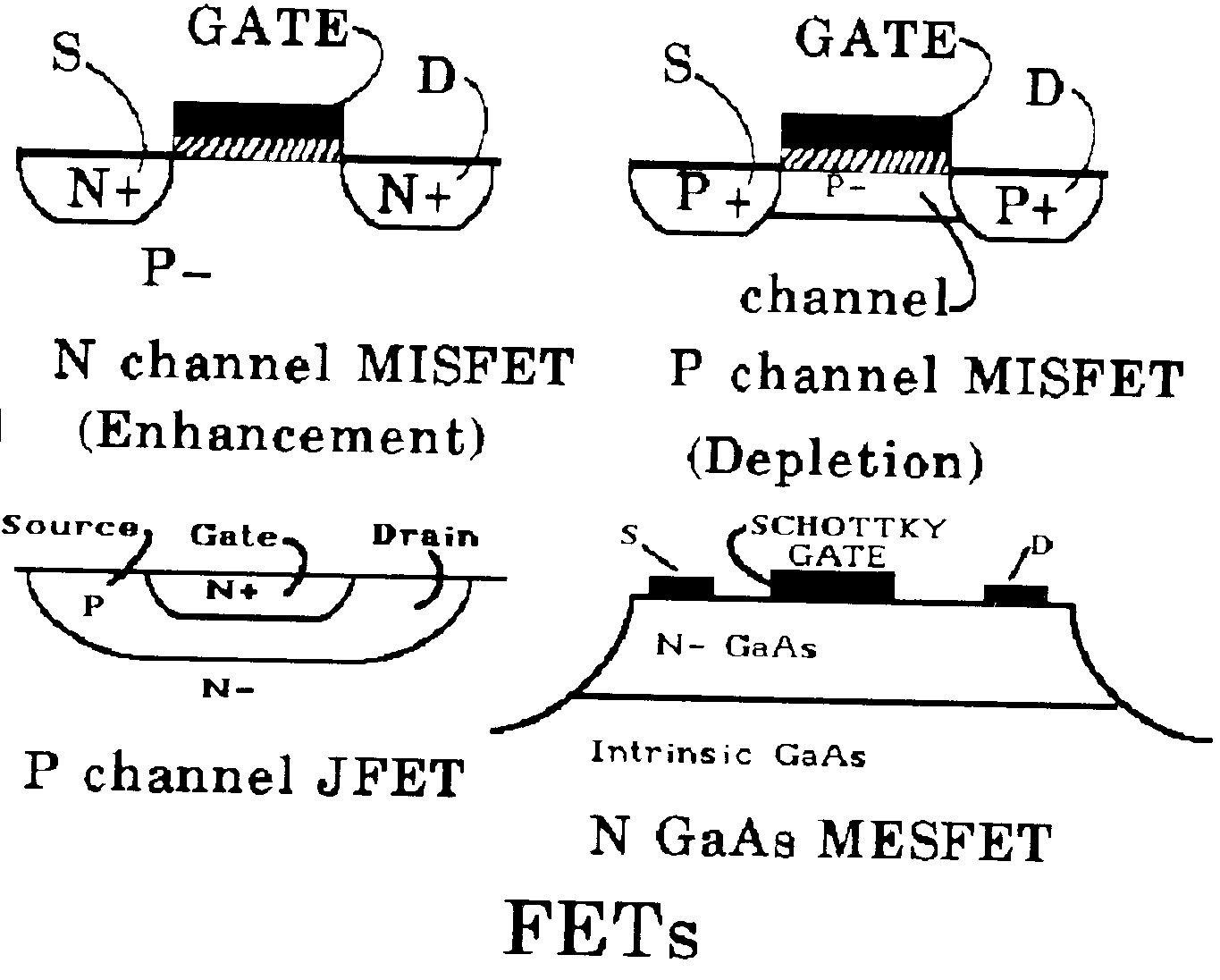
| 143 | Gettering of semiconductor substrate: | ||
| This subclass is indented under subclass 142. Process including a step of gettering the semiconductor
substrate.
SEE OR SEARCH THIS CLASS, SUBCLASS:
| |||
| 144 | Charge transfer device (e.g., CCD, etc.): | ||||||||||||||
This subclass is indented under subclass 142. Process for making a structure in which storage sites for
packets of electrical charge are induced at or below the semiconductor
surface by an electric field applied by serially arranged gate electrodes
formed thereupon and wherein carrier potential energy per unit charge
minima are established at a given storage site and such minima are
transferred in a serial manner via an active channel region to one
or more adjacent storage sites.
SEE OR SEARCH THIS CLASS, SUBCLASS:
SEE OR SEARCH CLASS:
| |||||||||||||||
| 145 | Having additional electrical device: |
| This subclass is indented under subclass 144. Process for making a charge transfer device structure in combination with an additional electrical device. | |
| 146 | Majority signal carrier (e.g., buried or bulk channel, peristaltic, etc.): |
| This subclass is indented under subclass 144. Process for making a charge transfer device structure wherein the transfer of such charge minima is by majority carriers of the semiconductive material (i.e., by electrons in n-type material, and is by holes in p-type semiconductive material). | |
| 147 | Changing width or direction of channel (e.g., meandering channel, etc.): |
| This subclass is indented under subclass 144. Process for making a charge transfer device structure wherein the active channel region changes its width or direction throughout all or part of the distance between adjacent storage sites. | |
| 148 | Substantially incomplete signal charge transfer (e.g., bucket brigade, etc.): |
| This subclass is indented under subclass 144. Process for making a charge transfer device structure wherein the charge transferred is less than the entire charge stored in the storage site from which it originates. | |
| 149 | On insulating substrate or layer (e.g., TFT, etc.): | ||
| This subclass is indented under subclass 142. Process for making a field effect transistor from a semiconductive
layer formed upon an insulating substrate (for example, glass
or sapphire) or an insulating layer.
SEE OR SEARCH THIS CLASS, SUBCLASS:
| |||
| 150 | Specified crystallographic orientation: |
| This subclass is indented under subclass 149. Process wherein a given feature of the field effect device on an insulating substrate or layer is formed in a definite crystallographic relationship relative to the insulating substrate or layer or the semiconductor layer thereupon. | |
| 151 | Having insulated gate: |
| This subclass is indented under subclass 149. Process for making an insulated gate field effect transistor from a semiconductive layer formed upon an insulating substrate (for example, glass or sapphire) or an insulating layer. | |
| 152 | Combined with electrical device not on insulating substrate or layer: | ||||||
This subclass is indented under subclass 151. Process for making a field effect transistor formed on an
insulating substrate or layer combined with an additional electrical
device which is not formed upon an insulating substrate or layer.
SEE OR SEARCH THIS CLASS, SUBCLASS:
SEE OR SEARCH CLASS:
| |||||||
| 153 | Complementary field effect transistors: |
| This subclass is indented under subclass 152. Process for making plural field effect transistors of opposite conductivity type (i.e., wherein source and drain regions of a first field effect transistor are of opposite conductivity type to source and drain regions of a second field effect transistor). | |
| 154 | Complementary field effect transistors: |
| This subclass is indented under subclass 151. Process for making plural field effect transistors of opposite conductivity type (i.e., wherein source and drain regions of a first field effect transistor are of opposite conductivity type to source and drain regions of a second field effect transistor). | |
| 155 | And additional electrical device on insulating substrate or layer: | ||||
This subclass is indented under subclass 151. Process for making a field effect transistor formed on an
insulating layer or substrate combined with an additional electrical
device which is also formed on an insulating substrate or layer.
SEE OR SEARCH THIS CLASS, SUBCLASS:
| |||||
| 156 | Vertical channel: |
| This subclass is indented under subclass 151. Process for making a junction gate field effect transistor wherein the active channel is configured to provide, in whole or in part, a vertically conductive pathway between source and drain regions. | |
| 157 | Plural gate electrodes (e.g., dual gate, etc.): | ||
| This subclass is indented under subclass 151. Process for making a field effect transistor formed on an
insulating layer or substrate wherein plural insulated gate electrodes
on either the same or opposite sides of the active channel region
serve to control the electrical conduction characteristics of the
semiconductive active channel region.
SEE OR SEARCH THIS CLASS, SUBCLASS:
| |||
| 158 | Inverted transistor structure: |
| This subclass is indented under subclass 151. Process for making a field effect transistor formed on an insulating substrate or layer wherein the gate electrode of the field effect transistor is formed so as to be in direct contact with the insulating substrate or layer. | |
| 159 | Source-to-gate or drain-to-gate overlap: |
| This subclass is indented under subclass 158. Process wherein the source or drain regions or layers of the inverted field effect transistor are formed so as to extend over a portion of the gate electrode formed on the insulating substrate or layer. | |
| 160 | Utilizing backside irradiation: |
| This subclass is indented under subclass 158. Process wherein single or multiple layers formed over the gate are patterned by irradiating a photoresist layer with a radiation source located on the opposite side of the substrate from which the gate is formed. | |
| 161 | Including source or drain electrode formation prior to semiconductor layer formation (i.e., staggered electrodes): |
| This subclass is indented under subclass 151. Process wherein the source or drain electrodes of the field effect transistor are formed on the insulating substrate or layer prior to the deposition of a semiconductive layer. | |
| 162 | Introduction of nondopant into semiconductor layer: |
| This subclass is indented under subclass 151. Process wherein a nonelectrically active impurity (i.e., one that does not change the electrically properties) is introduced into the semiconductive layer. | |
| 163 | Adjusting channel dimension (e.g., providing lightly doped source or drain region, etc.): |
| This subclass is indented under subclass 151. Process wherein a particular dimension of the active channel region of the field effect transistor (e.g., thickness, length, etc.) is adjusted. | |
| 164 | Semiconductor islands formed upon insulating substrate or layer (e.g., mesa formation, etc.): | ||
This subclass is indented under subclass 151. Process wherein the semiconductor layer selectively deposited
or deposited and subsequently patterned to form a semiconductive
region electrically isolated from laterally adjoining semiconductor
regions.
| |||
| 165 | Including differential oxidation: |
| This subclass is indented under subclass 164. Process in which the patterning of the semiconductive layer includes a step of oxidizing the semiconductive layer to form regions of differing oxide thickness. | |
| 166 | Including recrystallization step: | ||
| This subclass is indented under subclass 151. Process wherein the crystalline structure of the semiconductive
layer is altered or modified (e.g., from
amorphous to polycrystalline or single crystalline).
SEE OR SEARCH THIS CLASS, SUBCLASS:
| |||
| 167 | Having Schottky gate (e.g., MESFET, HEMT, etc.): |
| This subclass is indented under subclass 142. Process for making a field effect transistor which possesses a gate which forms a metal-semiconductor rectifying junction with the underlying semiconductive active channel region. | |
| 168 | Specified crystallographic orientation: | ||
This subclass is indented under subclass 167. Process wherein a given feature of the Schottky gate field
effect device is formed in a definite crystallographic orientation
relative to the substrate.
| |||
| 169 | Complementary Schottky gate field effect transistors: |
| This subclass is indented under subclass 167. Process for making plural Schottky gate field effect transistors of opposite conductivity type (i.e., wherein source and drain regions of a first field effect transistor are of opposite conductivity type to source and drain regions of a second field effect transistor). | |
| 170 | And bipolar device: |
| This subclass is indented under subclass 167. Process for making a bipolar transistor in addition to the Schottky gate field effect transistor. | |
| 171 | And passive electrical device (e.g., resistor, capacitor, etc.): |
| This subclass is indented under subclass 167. Process for making a Schottky gate field effect transistor having combined therewith an electrical device or element in which charge carriers do not change their energy levels and do not provide electrical rectification, amplification, or switching, but which does react to voltage and current input. | |
| 172 | Having heterojunction (e.g., HEMT, MODFET, etc.): |
| This subclass is indented under subclass 167. Process for making a Schottky gate field effect transistor wherein the Schottky gate field effect transistor possesses an interface between two dissimilar semiconductor materials which constitute a junction. | |
| 173 | Vertical channel: |
| This subclass is indented under subclass 167. Process for making a Schottky gate field effect transistor wherein the active channel is configured to provide, in whole or in part, a vertically conductive pathway between source and drain regions. | |
| 174 | Doping of semiconductive channel region beneath gate (e.g., threshold voltage adjustment, etc.): | ||
This subclass is indented under subclass 167. Process for making a Schottky gate field effect transistor
having a step of introducing an electrically active dopant species
into the semiconductor channel region beneath the gate electrode.
| |||
| 175 | Buried channel: |
| This subclass is indented under subclass 167. Process for making a Schottky gate field effect transistor wherein the channel formed between the source and drain regions is configured so as to be buried beneath the semiconductor substrate surface. | |
| 176 | Plural gate electrodes (e.g., dual gate, etc.): |
| This subclass is indented under subclass 167. Process for making a Schottky gate field effect transistor wherein plural gate electrodes on either the same or opposite side of the active channel region serve to control the electrical conduction characteristics of the semiconductive active channel region. | |
| 177 | Closed or loop gate: |
| This subclass is indented under subclass 167. Process for making a Schottky field effect transistor wherein the gate electrode is configured such that it closes upon itself to thereby totally surround one of the device active regions. | |
| 178 | Elemental semiconductor: |
| This subclass is indented under subclass 167. Process for making a Schottky gate field effect transistor wherein the gate electrode is formed upon an elemental semiconductor active channel region. | |
| 179 | Asymmetric: |
| This subclass is indented under subclass 167. Process for making a Schottky gate field effect transistor wherein the pair of active regions are off-set or nonsymmetrical with respect to the centerline of the Schottky gate electrode. | |
| 180 | Self-aligned: | ||
This subclass is indented under subclass 167. Process for making a Schottky gate field effect transistor
wherein a previously formed device feature is utilized to make device
regions in the desired registration to the previously formed feature.
| |||
| 181 | Doping of semiconductive region: |
| This subclass is indented under subclass 180. Process wherein a semiconductive region of the substrate is changed in electrical properties by introduction of an electrically active impurity. | |
| 182 | T-gate: |
| This subclass is indented under subclass 181. Process wherein a T-shaped gate structure is formed or utilized at any stage in the process. | |
| 183 | Dummy gate: |
| This subclass is indented under subclass 181. Process wherein a temporary gate is formed or utilized at any stage in the process and is intended to be removed or have no function in the final device. | |
| 184 | Utilizing gate sidewall structure: | ||
This subclass is indented under subclass 181. Process wherein a gate sidewall structure is utilized during
the doping of semiconductive regions adjacent the gate structure.
| |||
| 185 | Multiple doping steps: |
| This subclass is indented under subclass 184. Process including plural steps of doping the semiconductive regions of the substrate. | |
| 186 | Having junction gate (e.g., JFET, SIT, etc.): |
| This subclass is indented under subclass 142. Process for making a field effect transistor which possesses a gate electrode which forms a PN (rectifying) junction with the semiconductor active channel region. | |
| 187 | Specified crystallographic orientation: | ||
This subclass is indented under subclass 186. Process wherein a given feature of the junction gate field
effect device is formed in a definite crystallographic orientation
relative to the substrate.
| |||
| 188 | Complementary junction gate field effect transistors: |
| This subclass is indented under subclass 186. Process for making plural junction gate field effect transistors of opposite conductivity type (i.e., wherein source and drain regions of a first field effect transistor are of opposite conductivity type to source and drain regions of a second field effect transistor). | |
| 189 | And bipolar transistor: |
| This subclass is indented under subclass 186. Process for making a junction gate field effect transistor which additionally contains a bipolar transistor. | |
| 190 | And passive device (e.g., resistor, capacitor, etc.): |
| This subclass is indented under subclass 186. Process for making a junction gate field effect transistor having combined therewith an electrical device or component in which charge carriers do not change their energy levels and do not provide electrical rectification, amplification, or switching, but which does react to voltage and current input. | |
| 191 | Having heterojunction: |
| This subclass is indented under subclass 186. Process for making a junction gate field effect transistor which possesses an interface between two dissimilar semiconductor materials which constitute a junction. | |
| 192 | Vertical channel: | ||
| This subclass is indented under subclass 186. Process for making a junction gate field effect transistor
wherein the active channel is configured to provide, in
whole or in part, a vertically conductive pathway between
source and drain regions.
SEE OR SEARCH THIS CLASS, SUBCLASS:
| |||
| 193 | Multiple parallel current paths (e.g., grid gate, etc.): |
| This subclass is indented under subclass 192. Process for making a junction gate field effect transistor wherein the junction gate which controls the vertical channel consists of a plurality of parallel current paths. | |
| 194 | Doping of semiconductive channel region beneath gate (e.g., threshold voltage adjustment, etc.): | ||
This subclass is indented under subclass 186. Process for making a junction gate field effect transistor
having a step of introducing an electrically active dopant species
into the semiconductor channel region beneath the gate electrode.
| |||
| 195 | Plural gate electrodes: |
| This subclass is indented under subclass 186. Process for making a junction gate field effect transistor having plural gate electrodes on either the same or opposite side of the active channel region which serve to control the electrical conduction characteristics of the semiconductive active channel region. | |
| 196 | Including isolation structure: |
| This subclass is indented under subclass 186. Process for making a junction gate field effect transistor having a structure which serves to at least partially electrically isolate the semiconductor region in which the device is formed from laterally adjacent semiconductive regions. | |
| 197 | Having insulated gate (e.g., IGFET, MISFET, MOSFET, etc.): | ||||
| This subclass is indented under subclass 142. Process for making a field effect transistor wherein the
gate electrode is electrically insulated from the semiconductive
substrate, that portion of the semiconductive substrate
therebeneath being the active channel region separating source and
drain.
SEE OR SEARCH THIS CLASS, SUBCLASS:
| |||||
| 198 | Specified crystallographic orientation: | ||
This subclass is indented under subclass 197. Process wherein a given feature of the junction gate field
effect device is formed in a definite crystallographic orientation
relative to the substrate.
| |||
| 199 | Complementary insulated gate field effect transistors (i.e., CMOS): |
| This subclass is indented under subclass 197. Process for making plural insulated gate field effect transistors of opposite conductivity type (i.e., wherein source and drain regions of a first field effect transistor are of opposite conductivity type to source and drain regions of a second field effect transistor). | |
| 200 | And additional electrical device: |
| This subclass is indented under subclass 199. Process for making complementary insulated gate field effect transistors having combined therewith an additional electrical device. | |
| 201 | Including insulated gate field effect transistor having gate surrounded by dielectric (i.e., floating gate): | ||
This subclass is indented under subclass 200. Process for making complementary insulated gate field effect
transistors having combined therewith an additional insulated gate
field effect transistor possessing a gate electrode enclosed by
dielectric.
| |||
| 202 | Including bipolar transistor (i.e., BiCMOS): |
| This subclass is indented under subclass 200. Process for making complementary insulated gate field effect transistors combined with a bipolar transistor. | |
| 203 | Complementary bipolar transistors: |
| This subclass is indented under subclass 202. Process for making complementary insulated gate field effect transistors combined with a first bipolar transistor which additionally contains a second bipolar transistor which is of opposite conductivity type to the first bipolar transistor. | |
| 204 | Lateral bipolar transistor: |
| This subclass is indented under subclass 202. Process for making complementary insulated gate field effect transistors additionally having a bipolar transistor possessing a horizontal-type structure so that current flow between its emitter and collector regions is parallel to a major surface of the semiconductor substrate. | |
| 205 | Plural bipolar transistors of differing electrical characteristics: |
| This subclass is indented under subclass 202. Process for making complementary insulated gate field effect transistors combined with multiple bipolar transistors of differing electrical properties. | |
| 206 | Vertical channel insulated gate field effect transistor: |
| This subclass is indented under subclass 202. Process for making complementary insulated gate field effect transistors combined with a bipolar transistor and wherein at least one insulated gate field effect transistor possesses an active channel region which is configured to provide, at least in part, a vertically conductive pathway between source and drain regions. | |
| 207 | Including isolation structure: |
| This subclass is indented under subclass 202. Process for making complementary insulated gate field effect transistors combined with a bipolar transistor having a structure serving to at least partially electrically isolate the semiconductive region in which one transistor is formed from laterally adjacent semiconductive regions. | |
| 208 | Isolation by PN junction only: |
| This subclass is indented under subclass 207. Process for making complementary insulated gate field effect transistors combined with a bipolar transistor in which the transistors are electrically isolated solely through the use of properly biased PN junctions. | |
| 209 | Including additional vertical channel insulated gate field effect transistor: |
| This subclass is indented under subclass 200. Process for making complementary insulated gate field effect transistors having combined therewith an additional field effect transistor having an active channel region configured to provide, at least in part, a vertically conductive pathway between source and drain regions. | |
| 210 | Including passive device (e.g., resistor, capacitor, etc.): |
| This subclass is indented under subclass 200. Process for making complementary insulated gate field effect transistors having combined therewith a passive electrical device or element (i.e., an electrical device or component in which charge carriers do not change their energy levels and do not provide electrical rectification, amplification, or switching, but which does react to voltage and current input). | |
| 211 | Having gate surrounded by dielectric (i.e., floating gate): | ||
This subclass is indented under subclass 199. Process for making complementary insulated gate field effect
transistors wherein at least one field effect transistor has an
additional insulated gate electrode completely separated by dielectric
from its first insulated gate electrode.
| |||
| 212 | Vertical channel: | ||
| This subclass is indented under subclass 199. Process for making complementary insulated gate field effect
transistors wherein the active channel region of at least one of
the transistors is configured to provide, at least in part, a
vertically conductive pathway between source and drain regions.
SEE OR SEARCH THIS CLASS, SUBCLASS:
| |||
| 213 | Common active region: |
| This subclass is indented under subclass 199. Process for making complementary insulated gate field effect transistors wherein the transistors share a device active region. | |
| 214 | Having underpass or crossunder: |
| This subclass is indented under subclass 199. Process for making complementary insulated gate field effect transistors having an electrically conductive structure located within the semiconductor substrate which functions to electrically connect the transistors. | |
| 215 | Having fuse or integral short: |
| This subclass is indented under subclass 199. Process for making complementary field effect transistors having a structure which is alterable from the conductive to nonconductive state or functions to electrically short the transistor structure. | |
| 216 | Gate insulator structure constructed of diverse dielectrics (e.g., MNOS, etc.) or of nonsilicon compound: |
| This subclass is indented under subclass 199. Process for making complementary insulated gate field effect transistors wherein the gate dielectric insulator of at least one of the transistors is constructed of plural diverse dielectrics (e.g., nitride and oxide layers, etc.) or of a nonsilicon containing dielectric compound. | |
| 217 | Doping of semiconductor channel region beneath gate insulator (e.g., threshold voltage adjustment, etc.): |
| This subclass is indented under subclass 199. Process having a step of introducing an electrically active dopant species into the semiconductor active channel region beneath the gate insulator of at least one of the complementary insulated gate field effect transistors. | |
| 218 | Including isolation structure: |
| This subclass is indented under subclass 199. Process for making complementary field effect transistors having a structure serving to at least partially electrically isolate the semiconductive region in which one transistor is formed from laterally adjacent semiconductive regions. | |
| 219 | Total dielectric isolation: |
| This subclass is indented under subclass 218. Process for making complementary insulated gate field effect transistors in which at least one of the insulated gate complementary field effect transistors is fully electrically isolated by dielectric insulative material from laterally adjacent semiconductive regions. | |
| 220 | Isolation by PN junction only: |
| This subclass is indented under subclass 218. Process for making complementary insulated gate field effect transistors in which the transistors are electrically isolated solely through the use of properly biased PN junctions. | |
| 221 | Dielectric isolation formed by grooving and refilling with dielectric material: |
| This subclass is indented under subclass 218. Process for making complementary insulated gate field effect transistors wherein lateral isolation means is provided by forming a recess into the semiconductor substrate and refilling the recess at least in part with electrically insulative material. | |
| 222 | With epitaxial semiconductor layer formation: |
| This subclass is indented under subclass 221. Process for making complementary insulated gate field effect transistors with dielectric isolation formed by grooving and refilling with dielectric material including a step of forming an epitaxial semiconductor layer. | |
| 223 | Having well structure of opposite conductivity type: |
| This subclass is indented under subclass 221. Process for making complementary insulated gate field effect transistors including a step of forming a well of opposite conductivity to the adjoining semiconductor region in which well is formed an insulated gate field effect transistor of opposite conductivity type to an insulated gate field effect transistor located in the adjoining semiconductor region. | |
| 224 | Plural wells: |
| This subclass is indented under subclass 223. Process for making complementary insulated gate field effect transistors wherein plural wells of the same or opposite conductivity type are formed in the semiconductive substrate, each well utilized for formation therein of an insulated gate field effect transistor. | |
| 225 | Recessed oxide formed by localized oxidation (i.e., LOCOS): |
| This subclass is indented under subclass 218. Process for making complementary insulated gate field effect transistors wherein lateral isolation means is provided by a step of selectively oxidizing semiconductive regions of the substrate. | |
| 226 | With epitaxial semiconductor layer formation: |
| This subclass is indented under subclass 225. Process for making complementary insulated gate field effect transistors with dielectric isolation formed by selectively oxidizing semiconductive regions of the substrate combined with a step of forming an epitaxial semiconductor layer. | |
| 227 | Having well structure of opposite conductivity type: |
| This subclass is indented under subclass 225. Process for making complementary insulated gate field effect transistors including a step of forming a well of opposite conductivity to the adjoining semiconductor regions in which well is formed an insulated gate field effect transistor of opposite conductivity type to an insulated gate field effect transistor located in the adjoining semiconductor region. | |
| 228 | Plural wells: |
| This subclass is indented under subclass 227. Process for making complementary insulated gate field effect transistors wherein plural wells of the same or opposite conductivity type are formed in the semiconductive substrate, each well utilized for formation therein of an insulated gate field effect transistor. | |
| 229 | Self-aligned: | ||
This subclass is indented under subclass 199. Process for making complementary insulated gate field effect
transistors wherein a previously formed device feature is utilized
to make device regions in the desired registration to the previously
formed feature.
| |||
| 230 | Utilizing gate sidewall structure: |
| This subclass is indented under subclass 229. Process with a step of utilizing a structure located on the sidewall of the gate electrode as the previously formed device feature. | |
| 231 | Plural doping steps: |
| This subclass is indented under subclass 230. Process including multiple steps of introducing electrically active dopant species into semiconductor regions of the substrate. | |
| 232 | Plural doping steps: |
| This subclass is indented under subclass 229. Process including multiple steps of introducing electrically active dopant species into semiconductor regions of the substrate. | |
| 233 | And contact formation: |
| This subclass is indented under subclass 199. Process for making complementary insulated gate field effect transistors including a step of forming electrical connections to the transistors. | |
| 234 | Including bipolar transistor (i.e., BiMOS): |
| This subclass is indented under subclass 197. Process for making an insulated gate field effect transistor having combined therewith a bipolar transistor. | |
| 235 | Heterojunction bipolar transistor: |
| This subclass is indented under subclass 234. Process for making an insulated gate field effect transistor combined with a bipolar transistor wherein the emitter-base junction or the collector-base junction of the bipolar transistor possesses an interface between two dissimilar semiconductor materials. | |
| 236 | Lateral bipolar transistor: |
| This subclass is indented under subclass 234. Process for making an insulated gate field effect transistor combined with a bipolar transistor which has a horizontal-type structure resulting in current flow between its emitter and collector regions parallel to a major surface of the semiconductor substrate. | |
| 237 | Including diode: |
| This subclass is indented under subclass 197. Process for making an insulated gate field effect transistor having combined therewith a diode device or element. | |
| 238 | Including passive device (e.g., resistor, capacitor, etc.): | ||
| This subclass is indented under subclass 197. Process for making an insulated gate field effect transistor
having combined therewith an electrical device or component in which
charge carriers do not change their energy levels and do not provide
electrical rectification, amplification, or switching, but
which does react to voltage and current input.
SEE OR SEARCH THIS CLASS, SUBCLASS:
| |||
| 239 | Capacitor: |
| This subclass is indented under subclass 238. Process for making an insulated gate field effect transistor having combined therewith a capacitor as the passive device. | |
| 240 | Having high dielectric constant insulator (e.g., Ta2O5, etc.): |
| This subclass is indented under subclass 239. Process wherein the capacitor dielectric is constructed of a material having a dielectric constant of greater than 7.5, the dielectric constant of Si3N4. | |
| 241 | And additional field effect transistor (e.g., sense or access transistor, etc.): | ||
| This subclass is indented under subclass 239. Process for making an insulated gate field effect transistor
having combined therewith a capacitor and an additional field effect
transistor.
SEE OR SEARCH THIS CLASS, SUBCLASS:
| |||
| 242 | Including transistor formed on trench sidewalls: | ||
This subclass is indented under subclass 241. Process wherein the additional diverse field effect transistor
is formed on the side-walls of a groove formed in the semiconductor
substrate.
| |||
| 243 | Trench capacitor: | ||
| This subclass is indented under subclass 239. Process for making an insulated gate field effect transistor
combined with a capacitor which is located in a groove in the semiconductor
substrate.
SEE OR SEARCH CLASS:
| |||
| 244 | Utilizing stacked capacitor structure (e.g., stacked trench, buried stacked capacitor, etc.): |
| This subclass is indented under subclass 243. Process wherein the trench capacitor contains a number of capacitor plate regions aligned vertically above each other or wherein the capacitor and the insulated gate field effect transistor are located such that one overlies the other. | |
| 245 | With epitaxial layer formed over the trench: |
| This subclass is indented under subclass 243. Process including a step of forming an epitaxial semiconductive layer over the trench region. | |
| 246 | Including doping of trench surfaces: | ||
| This subclass is indented under subclass 243. Process having a step of introducing electrically active
dopant species into the surfaces of the groove in which the capacitor
is located.
SEE OR SEARCH THIS CLASS, SUBCLASS:
| |||
| 247 | Multiple doping steps: |
| This subclass is indented under subclass 246. Process utilizing plural steps of introducing electrically active dopant species into the trench surfaces. | |
| 248 | Including isolating means formed in trench: |
| This subclass is indented under subclass 246. Process including forming a structure functioning as electrical isolation means at the groove bottom. | |
| 249 | Doping by outdiffusion from a dopant source layer (e.g., doped oxide, etc.): |
| This subclass is indented under subclass 246. Process wherein doping the trench surfaces is via diffusion from an adjacent dopant source layer formed thereupon. | |
| 250 | Planar capacitor: |
| This subclass is indented under subclass 239. Process for making an insulated gate field effect transistor combined with a capacitor wherein a generally planar region of the semiconductive substrate forms a first capacitor plate with the capacitor dielectric and a second capacitor plate formed thereupon. | |
| 251 | Including doping of semiconductive region: |
| This subclass is indented under subclass 250. Process having a step of introducing an electrically active dopant species into a semiconductive region of the substrate forming the first capacitor plate. | |
| 252 | Multiple doping steps: |
| This subclass is indented under subclass 251. Process having plural steps of introducing electrically active dopant species into a semiconductive region of the substrate forming the first capacitor plate. | |
| 253 | Stacked capacitor: | ||
| This subclass is indented under subclass 239. Process for making an insulated gate field effect transistor
in combination with a capacitor containing a number of capacitor
plate and dielectric layers deposited successively one atop another
and overlying the field effect transistor.
SEE OR SEARCH CLASS:
| |||
| 254 | Including selectively removing material to undercut and expose storage node layer: | ||
This subclass is indented under subclass 253. Process having a step of selectively removing material (e.g., by
etching, etc.) to undercut and expose
the capacitor electrode which serves as the storage node layer of
the stacked capacitor.
| |||
| 255 | Including texturizing storage node layer: | ||
This subclass is indented under subclass 253. Process having a step of roughening the surface of the capacitor
plate which serves as the storage node layer of the stacked capacitor.
| |||
| 256 | Contacts formed by selective growth or deposition: |
| This subclass is indented under subclass 253. Process wherein electrical contacts are formed by selective growth or deposition of conductive material onto the semiconductor substrate. | |
| 257 | Having additional gate electrode surrounded by dielectric (i.e., floating gate): | ||||
This subclass is indented under subclass 197. Process for making an insulated gate field effect transistor
wherein an additional gate electrode completely separated by dielectric from
a first insulated gate electrode is formed.
SEE OR SEARCH THIS CLASS, SUBCLASS:
| |||||
| 258 | Including additional field effect transistor (e.g., sense or access transistor, etc.): | ||
| This subclass is indented under subclass 257. Process for making a floating gate-type insulated
gate field effect transistor having combined therewith an additional
field effect transistor.
SEE OR SEARCH THIS CLASS, SUBCLASS:
| |||
| 259 | Including forming gate electrode in trench or recess in substrate: |
| This subclass is indented under subclass 257. Process for making a floating gate type insulated gate field effect transistor including forming a gate electrode in a groove located in the semiconductor substrate. | |
| 260 | Textured surface of gate insulator or gate electrode: |
| This subclass is indented under subclass 257. Process for making a floating gate-type insulated gate field effect transistor wherein a roughened surface is utilized for the gate insulator or gate electrode. | |
| 261 | Multiple interelectrode dielectrics or nonsilicon compound gate insulator: | ||
| This subclass is indented under subclass 257. Process for making a floating gate-type insulated
gate field effect transistor with plural interelectrode dielectrics
or a nonsilicon compound dielectric material.
SEE OR SEARCH THIS CLASS, SUBCLASS:
| |||
| 262 | Including elongated source or drain region disposed under thick oxide regions (e.g., buried or diffused bitline, etc.): | ||||
This subclass is indented under subclass 257. Process for making a floating gate-type insulated
gate field effect transistor having elongated source or drain region
located under thick oxide dielectric regions.
SEE OR SEARCH THIS CLASS, SUBCLASS:
| |||||
| 263 | Tunneling insulator: |
| This subclass is indented under subclass 262. Process for making a floating gate type insulated gate field effect transistor including an insulative layer adjacent the gate electrode which allows passage of charge carriers therethrough. | |
| 264 | Tunneling insulator: |
| This subclass is indented under subclass 257. Process for making a floating gate-type insulated gate field effect transistor including an insulative layer adjacent the gate electrode which allows passage of charge carriers therethrough. | |
| 265 | Oxidizing sidewall of gate electrode: |
| This subclass is indented under subclass 257. Process for making a floating gate-type field effect transistor including a step of forming a dielectric sidewall on the gate electrode by reacting the gate electrode material with oxygen. | |
| 266 | Having additional, nonmemory control electrode or channel portion (e.g., for accessing field effect transistor structure, etc.): | ||
| This subclass is indented under subclass 257. Process for making a floating gate-type field effect
transistor having an additional, nonmemory control electrode (i.e., having
direct electrical contact thereto) or channel portion.
SEE OR SEARCH CLASS:
| |||
| 267 | Including forming gate electrode as conductive sidewall spacer to another electrode: |
| This subclass is indented under subclass 266. Process including a step of forming a conductive electrode on the sidewall of another electrode wherein the conductive sidewall serves as a gate electrode. | |
| 268 | Vertical channel: |
| This subclass is indented under subclass 197. Process for making a insulated gate field effect transistor wherein the active channel is configured to provide, in whole or in part, a vertically conductive pathway between source and drain regions. | |
| 269 | Utilizing epitaxial semiconductor layer grown through an opening in an insulating layer: |
| This subclass is indented under subclass 268. Process for making an insulated gate field effect transistor wherein a epitaxial semiconductor layer is deposited through an opening in an insulating layer upon a semiconductor substrate. | |
| 270 | Gate electrode in trench or recess in semiconductor substrate: | ||
| This subclass is indented under subclass 268. Process for making an insulated gate field effect transistor
wherein the gate electrode is formed in a groove or recess in the
semiconductor substrate.
SEE OR SEARCH THIS CLASS, SUBCLASS:
| |||
| 271 | V-gate: |
| This subclass is indented under subclass 270. Process for making an insulated gate field effect transistor wherein the gate electrode has a V-shape configuration. | |
| 272 | Totally embedded in semiconductive layers: |
| This subclass is indented under subclass 270. Process wherein the gate electrode is surrounded on all sides by semiconductive layers. | |
| 273 | Having integral short of source and base regions: |
| This subclass is indented under subclass 268. Process for making an insulated gate field effect transistor having an integral electrical connection between the source and base (i.e., substrate) regions. | |
| 274 | Short formed in recess in substrate: |
| This subclass is indented under subclass 273. Process wherein the integral short is formed in a groove in the semiconductor substrate | |
| 275 | Making plural insulated gate field effect transistors of differing electrical characteristics: | ||
| This subclass is indented under subclass 197. Process for making multiple insulated gate field effect
transistors of differing electrical characteristics.
SEE OR SEARCH THIS CLASS, SUBCLASS:
| |||
| 276 | Introducing a dopant into the channel region of selected transistors: | ||||
| This subclass is indented under subclass 275. Process for making plural insulated gate field effect transistors
having a step of introducing an electrically active dopant species
into the semiconductor channel region beneath the gate insulator
of one or more transistors to produce transistors of differing electrical
characteristics.
SEE OR SEARCH THIS CLASS, SUBCLASS:
| |||||
| 277 | Including forming overlapping gate electrodes: |
| This subclass is indented under subclass 276. Process for making plural insulated gate field effect transistors of differing electrical characteristics including a step of forming overlapping gate electrodes. | |
| 278 | After formation of source or drain regions and gate electrode (e.g., late programming, encoding, etc.): |
| This subclass is indented under subclass 276. Process for making plural insulated gate field effect transistors of differing electrical characteristics wherein the semiconductor channel region is doped subsequent to the formation of the source and drain regions and the gate electrode. | |
| 279 | Making plural insulated gate field effect transistors having common active region: |
| This subclass is indented under subclass 197. Process for making multiple insulated gate field effect transistors in which a transistor active region is shared between two or more field effect transistors. | |
| 280 | Having underpass or crossunder: | ||
| This subclass is indented under subclass 197. Process for making an insulated gate field effect transistor
electrically interconnected to an adjoining electrical device via
a conductive structure located within the semiconductor substrate.
SEE OR SEARCH THIS CLASS, SUBCLASS:
| |||
| 281 | Having fuse or integral short: | ||||
| This subclass is indented under subclass 197. Process for making an insulated gate field effect transistor
which possesses a structure alterable to a nonconductive state (i.e., fuse) or an
integral electrical connection between source and gate regions or
between drain and gate regions.
SEE OR SEARCH THIS CLASS, SUBCLASS:
| |||||
| 282 | Buried channel: |
| This subclass is indented under subclass 197. Process for making an insulated gate field effect transistor wherein the channel formed between the source and drain regions is configured so as to be located beneath the semiconductor substrate surface. | |
| 283 | Plural gate electrodes (e.g., dual gate, etc.): | ||
| This subclass is indented under subclass 197. Process for making an insulated gate field effect transistor
wherein plural gate electrodes on either the same or opposite side
of the active channel region serve to control the electrical conduction
characteristics of the semiconductive active channel region.
SEE OR SEARCH THIS CLASS, SUBCLASS:
| |||
| 284 | Closed or loop gate: |
| This subclass is indented under subclass 197. Process for making an insulated gate field effect transistor wherein the gate electrode is configured such that it closes upon itself to thereby totally surround one of the device active regions. | |
| 285 | Utilizing compound semiconductor: |
| This subclass is indented under subclass 197. Process for making an insulated gate field effect transistor utilizing a compound semiconductor active region. | |
| 286 | Asymmetric: |
| This subclass is indented under subclass 197. Process for making an insulated gate field effect transistor wherein the pair of active regions are offset or nonsymmetrical with respect to the centerline of the insulated gate electrode. | |
| 287 | Gate insulator structure constructed of diverse dielectrics (e.g., MNOS, etc.) or of nonsilicon compound: | ||||
| This subclass is indented under subclass 197. Process for making an insulated gate field effect transistor
wherein the gate dielectric insulator is constructed of plural diverse
dielectrics (e.g., nitride and
oxide, etc.) or of a nonsilicon containing
dielectric compound.
SEE OR SEARCH THIS CLASS, SUBCLASS:
| |||||
| 288 | Having step of storing electrical charge in gate dielectric: |
| This subclass is indented under subclass 197. Process for making an insulated gate field effect transistor having an active step of storing electrical charge in the gate dielectric insulator. | |
| 289 | Doping of semiconductive channel region beneath gate insulator (e.g., adjusting threshold voltage, etc.): | ||
| This subclass is indented under subclass 197. Process for making an insulated gate field effect transistor
having a step of introducing electrically active dopant species
into the semiconductor active channel region beneath the gate insulator.
SEE OR SEARCH THIS CLASS, SUBCLASS:
| |||
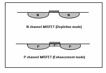
| 290 | After formation of source or drain regions and gate electrode: |
| This subclass is indented under subclass 289. Process wherein the semiconductor channel region is doped subsequent to the formation of the source and drain regions and the gate electrode. | |
| 291 | Using channel conductivity dopant of opposite type as that of source and drain: |
| This subclass is indented under subclass 289. Process wherein the dopant and the semiconductor active channel region beneath the gate insulator are of the same conductivity type. | |
| 292 | Direct application of electrical current: | ||
| This subclass is indented under subclass 197. Process for making an insulated gate field effect transistor
having a step of directly applying an electrical current to the
semiconductor substrate.
SEE OR SEARCH THIS CLASS, SUBCLASS:
| |||
| 293 | Fusion or solidification of semiconductor region: |
| This subclass is indented under subclass 197. Process for making an insulated gate field effect transistor having a step of fusing or solidifying a semiconductive region of the substrate. | |
| 294 | Including isolation structure: | ||
| This subclass is indented under subclass 197. Process for making an insulated gate field effect transistor
having a structure which serves to at least partially electrically
isolate the semiconductor region in which the device is formed from
laterally adjacent semiconductive regions.
SEE OR SEARCH THIS CLASS, SUBCLASS:
| |||
| 295 | Total dielectric isolation: |
| This subclass is indented under subclass 294. Process for making an insulated gate field effect transistor which is fully electrically isolated by dielectric insulative material from laterally adjacent semiconductive regions. | |
| 296 | Dielectric isolation formed by grooving and refilling with dielectric material: |
| This subclass is indented under subclass 294. Process for making an insulated gate field effect transistor including the step of forming an isolation structure by making a recess in the semiconductor substrate and refilling the recess with an insulative material. | |
| 297 | Recessed oxide formed by localized oxidation (i.e., LOCOS): |
| This subclass is indented under subclass 294. Process for making an insulated gate field effect transistor including the step of oxidizing a selected region of a semiconductive substrate to form an embedded oxide (e.g., field oxide) therein which forms the periphery of a semiconductive region utilized for the formation of the field effect transistor. | |
| 298 | Doping region beneath recessed oxide (e.g., to form chanstop, etc.): |
| This subclass is indented under subclass 297. Process including a step of introducing electrically active dopant species into the semiconductor substrate region beneath the recessed oxide (e.g., to form a channel stop thereby preventing electric field inversion beneath the recessed oxide, etc.). | |
| 299 | Self-aligned: | ||
This subclass is indented under subclass 197. Process for making an insulated gate field effect transistor
wherein a previously formed device feature is utilized to make device regions
in the desired registration to the previously formed feature.
| |||
| 300 | Having elevated source or drain (e.g., epitaxially formed source or drain, etc.): |
| This subclass is indented under subclass 299. Process including a step of forming the source or drain active region at a position above and laterally adjacent to the channel region of the transistor. | |
| 301 | Source or drain doping: |
| This subclass is indented under subclass 299. Process having a step for the self-aligned introduction of electrically active dopant species into the semiconductor regions of the substrate to form the transistor source or drain regions or portions thereof. | |
| 302 | Oblique implantation: |
| This subclass is indented under subclass 301. Process involving implanting ions other than perpendicularly with respect to the plane of the substrate. | |
| 303 | Utilizing gate sidewall structure: |
| This subclass is indented under subclass 301. Process having structure on the sidewall of the gate electrode or gate insulator which is utilized as the previously formed device feature. | |
| 304 | Conductive sidewall component: |
| This subclass is indented under subclass 303. Process wherein the gate sidewall structure is composed at least in part of a conductive component. | |
| 305 | Plural doping steps: |
| This subclass is indented under subclass 303. Process including multiple steps of introducing dopant species into the semiconductive regions of the substrate. | |
| 306 | Plural doping steps: |
| This subclass is indented under subclass 301. Process including multiple steps of introducing dopant species into the semiconductive regions of the substrate. | |
| 307 | Using same conductivity-type dopant: |
| This subclass is indented under subclass 306. Process wherein the same conductivity-type electrically active dopant is introduced using plural doping steps. | |
| 308 | Radiation or energy treatment modifying properties of semiconductor regions of substrate (e.g., thermal, corpuscular, electromagnetic, etc.): | ||
| This subclass is indented under subclass 197. Process for making an insulated gate field effect transistor
having a step of irradiating the semiconductor substrate to alter
the electrical properties of semiconductive regions thereof.
SEE OR SEARCH THIS CLASS, SUBCLASS:
| |||
| 309 | FORMING BIPOLAR TRANSISTOR BY FORMATION OR ALTERATION OF SEMICONDUCTIVE ACTIVE REGIONS: | ||||||||||||||
| This subclass is indented under the class definition. Process for forming a transistor structure which upon completion
possesses a base region separating two or more active regions and
in which both positive and negative charge carriers are used to
support current flow.
SEE OR SEARCH THIS CLASS, SUBCLASS:
SEE OR SEARCH CLASS:
| |||||||||||||||
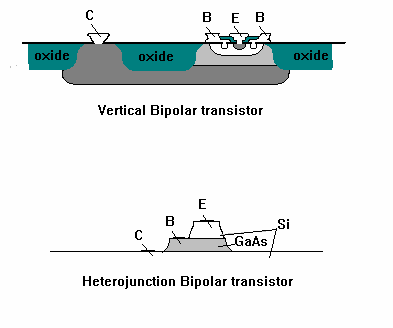
| 310 | Gettering of semiconductor substrate: |
| This subclass is indented under subclass 309. Process having a step of gettering the semiconductor substrate. | |
| 311 | On insulating substrate or layer (i.e., SOI type): |
| This subclass is indented under subclass 309. Process for making a bipolar transistor wherein the transistor is formed upon an insulating substrate (e.g., glass, sapphire, etc.) or layer. | |
| 312 | Having heterojunction: | ||||
| This subclass is indented under subclass 309. Process for making a bipolar transistor wherein the emitter-base
or the collector-base junction is an interface of two dissimilar
semiconductor materials resulting in a heterojunction therebetween.
SEE OR SEARCH THIS CLASS, SUBCLASS:
SEE OR SEARCH CLASS:
| |||||
| 313 | Complementary bipolar transistors: |
| This subclass is indented under subclass 312. Process for making a structure which comprises plural bipolar transistors wherein the emitter and collector regions of a first bipolar transistor are of opposite conductivity type to the emitter and collector regions of a second bipolar transistor.(i.e., both pnp and npn bipolar transistor structures), at least one of which possesses a heterojunction. | |
| 314 | And additional electrical device: |
| This subclass is indented under subclass 312. Process for making a heterojunction bipolar transistor and an additional electrical device. | |
| 315 | Forming inverted transistor structure: |
| This subclass is indented under subclass 312. Process forming a heterojunction bipolar transistor structure in which a semiconductor body such as a semiconductor substrate or a semiconductor layer is used as its emitter region, a first semiconductor region formed in the semiconductor body is used as the base region and a second semiconductor region formed in the first semiconductor region is used as the collector region. | |
| 316 | Forming lateral transistor structure: |
| This subclass is indented under subclass 312. Process for making a heterojunction bipolar transistor which has a horizontal structure resulting in current flow between its emitter and collector parallel to a major surface of the semiconductor substrate. | |
| 317 | Wide bandgap emitter: | ||
| This subclass is indented under subclass 312. Process for making a heterojunction bipolar transistor with
an active region which involves a charge carrier emitter region
made of a semiconductor material having an energy gap between its
conduction and valence band which is greater than the energy gap
of the dissimilar semiconductor material of the base region.
SEE OR SEARCH CLASS:
| |||
| 318 | Including isolation structure: | ||
| This subclass is indented under subclass 312. Process for making a heterojunction bipolar transistor which
has structure so as to at least partially electrically isolate the
device from laterally adjacent semiconductor regions.
SEE OR SEARCH THIS CLASS, SUBCLASS:
| |||
| 319 | Air isolation (e.g., mesa, etc.): | ||
| This subclass is indented under subclass 318. Process for making a heterojunction bipolar transistor wherein
the emitter or collector region of the device is a raised feature
with respect to the plane of the substrate.
SEE OR SEARCH THIS CLASS, SUBCLASS:
| |||
| 320 | Self-aligned: |
| This subclass is indented under subclass 312. Process for making a heterojunction bipolar transistor wherein a previously formed device feature is utilized to make device regions in the desired registration to the previously formed feature. | |
| 321 | Utilizing dummy emitter: |
| This subclass is indented under subclass 320. Process for making a heterojunction bipolar transistor wherein a substitute emitter is formed or removed prior to the forming of the active emitter region of the device. | |
| 322 | Complementary bipolar transistors: |
| This subclass is indented under subclass 309. Process for making plural bipolar transistors wherein the emitter and collector regions or a first bipolar transistor are of opposite conductivity type to the emitter and collector regions of a second bipolar transistor. | |
| 323 | Having common active region (i.e., integrated injection logic (I2L), etc.): |
| This subclass is indented under subclass 322. Process for making complementary bipolar transistors which possess a common active region. | |
| 324 | Including additional electrical device: |
| This subclass is indented under subclass 323. Process for making complementary bipolar transistors with shared common region having combined therewith an additional electrical device. | |
| 325 | Having lateral bipolar transistor: |
| This subclass is indented under subclass 323. Process for making complementary bipolar transistors with shared common region wherein at least one of the bipolar transistors has a horizontal structure resulting in current flow between its emitter and collector parallel to a major surface of the semiconductor substrate. | |
| 326 | Including additional electrical device: |
| This subclass is indented under subclass 322. Process for making complementary bipolar transistors having combined therewith an additional electrical device. | |
| 327 | Having lateral bipolar transistor: |
| This subclass is indented under subclass 322. Process for making complementary bipolar transistors wherein at least one of the bipolar transistors has a horizontal structure resulting in current flow between its emitter and collector parallel to a major surface of the semiconductor substrate. | |
| 328 | Including diode: |
| This subclass is indented under subclass 309. Process for making a bipolar transistor having combined therewith a diode. | |
| 329 | Including passive device (e.g., resistor, capacitor, etc.): |
| This subclass is indented under subclass 309. Process for making a bipolar transistor having combined therewith an electrical device or component in which charge carriers do not change their energy levels and do not provide electrical rectification, amplification, or switching, but which does react to voltage and current input. | |
| 330 | Resistor: | ||
| This subclass is indented under subclass 329. Process for making a bipolar transistor combined with a
resistive element or component.
SEE OR SEARCH CLASS:
| |||
| 331 | Having same doping as emitter or collector: | ||
This subclass is indented under subclass 330. Process wherein the resistor region has the same doping
profile (i.e., is formed in
the same step) as either the emitter or collector region
of the bipolar transistor with which the resistor is combined.
| |||
| 332 | Lightly doped junction isolated resistor: | ||
This subclass is indented under subclass 330. Process wherein the resistive element is in the form of
a lightly doped layer of one conductivity type located in a region
of opposite conductivity type, such that the pn junction
between the resistor region and its containing opposite conductivity-type
region serves to electrically isolate the resistor.
| |||
| 333 | Having fuse or integral short: | ||
| This subclass is indented under subclass 309. Process for making a bipolar transistor which possesses
a structure which is alterable from a conductive to a nonconductive
state (i.e., fuse) or
an integral electrical short between the collector and emitter active
regions or between the base and emitter active regions.
SEE OR SEARCH THIS CLASS, SUBCLASS:
| |||
| 334 | Forming inverted transistor structure: | ||
| This subclass is indented under subclass 309. Process forming a bipolar transistor structure in which
a semiconductor body such as a semiconductor substrate or a semiconductor
layer is used as its emitter region, a first semiconductor region
formed in the semiconductor body is used as the base region and
a second semiconductor region formed in the first semiconductor region
is used as the collector region.
SEE OR SEARCH THIS CLASS, SUBCLASS:
| |||
| 335 | Forming lateral transistor structure: | ||||||||
| This subclass is indented under subclass 309. Process for making a bipolar transistor wherein the transistor
has a horizontal structure resulting in current flow between its
emitter and collector parallel to a major surface of the semiconductor
substrate.
SEE OR SEARCH THIS CLASS, SUBCLASS:
SEE OR SEARCH CLASS:
| |||||||||
| 336 | Combined with vertical bipolar transistor: |
| This subclass is indented under subclass 335. Process for making a lateral bipolar transistor combined with a vertical bipolar transistor having current flow between its emitter and collector perpendicular to a major surface of the semiconductor substrate. | |
| 337 | Active region formed along groove or exposed edge in semiconductor: |
| This subclass is indented under subclass 335. Process for making a lateral bipolar transistor wherein the transistor has a recess or exposed edge and an active region of the transistor is formed along the recess or exposed edge. | |
| 338 | Having multiple emitter or collector structure: |
| This subclass is indented under subclass 335. Process for making a lateral bipolar transistor having plural emitter active regions or plural collector active regions. | |
| 339 | Self-aligned: |
| This subclass is indented under subclass 335. Process for making a lateral bipolar transistor wherein a previously formed device feature is utilized to make device active regions in the desired registration to the previously formed feature. | |
| 340 | Making plural bipolar transistors of differing electrical characteristics: |
| This subclass is indented under subclass 309. Process for making multiple bipolar transistors possessing differing electrical properties. | |
| 341 | Using epitaxial lateral overgrowth: | ||
| This subclass is indented under subclass 309. Process for making a bipolar transistor including forming
a single crystalline semiconductor layer epitaxially on the semiconductor
substrate and laterally over an insulative layer thereupon.
SEE OR SEARCH THIS CLASS, SUBCLASS:
| |||
| 342 | Having multiple emitter or collector structure: | ||
| This subclass is indented under subclass 309. Process for making a bipolar transistor having plural emitter
active regions or plural collector active regions.
SEE OR SEARCH CLASS:
| |||
| 343 | Mesa or stacked emitter: | ||
| This subclass is indented under subclass 309. Process for making a bipolar transistor wherein the emitter
is a raised feature relative to the adjoining semiconductive regions.
SEE OR SEARCH CLASS:
| |||
| 344 | Washed emitter: |
| This subclass is indented under subclass 309. Process wherein the surface of the semiconductive substrate is etched to remove oxide layers formed on the emitter region during emitter diffusion thus allowing an aperature used for diffusing the emitter impurity to be directly utilized as the aperature for electrical contact formation. | |
| 345 | Walled emitter: | ||
| This subclass is indented under subclass 309. Process for making a bipolar transistor wherein the emitter-base
junction terminates against a dielectric isolation sidewall.
SEE OR SEARCH CLASS:
| |||
| 346 | Emitter dip prevention or utilization: |
| This subclass is indented under subclass 309. Process involving special diffusion techniques to eliminate or utilize the tendency of the base-collector junction to "bulge" downward during the emitter diffusion. | |
| 347 | Permeable or metal base: | ||
| This subclass is indented under subclass 309. Process for making a bipolar transistor wherein the base
region incompletely separates the collector and emitter regions, or
is constructed of a metallic material.
SEE OR SEARCH THIS CLASS, SUBCLASS:
| |||
| 348 | Sidewall base contact: |
| This subclass is indented under subclass 309. Process for making a bipolar transistor wherein a conductive layer serving as the base electrode makes contact to the sidewall of the base region. | |
| 349 | Pedestal base: |
| This subclass is indented under subclass 309. Process for making a bipolar transistor wherein the base region is provided with a projecting portion. | |
| 350 | Forming base region of specified dopant concentration profile (e.g., inactive base region more heavily doped than active base region, etc.): | ||
| This subclass is indented under subclass 309. Process for making a bipolar transistor with a semiconductor
base region possessing a specified concentration profile of an electrically active
dopant species contained therein.
SEE OR SEARCH CLASS:
| |||
| 351 | Direct application of electrical current: | ||
| This subclass is indented under subclass 309. Process for making a bipolar transistor involving having
a step of directly applying an electric current to the semiconductor
substrate.
SEE OR SEARCH THIS CLASS, SUBCLASS:
| |||
| 352 | Fusion or solidification of semiconductor region: |
| This subclass is indented under subclass 309. Process for making a bipolar transistor having a step of fusing or solidifying semiconductive regions of the substrate. | |
| 353 | Including isolation structure: | ||
| This subclass is indented under subclass 309. Process for making a bipolar transistor having a structure
which serves to at least partially electrically isolate the semiconductive
region in which the transistor is formed from laterally adjacent
semiconductive regions.
SEE OR SEARCH THIS CLASS, SUBCLASS:
| |||
| 354 | Having semi-insulative region: |
| This subclass is indented under subclass 353. Process for making a bipolar transistor wherein the electrical isolation is provided at least in part by a high resistivity semiconductive component. | |
| 355 | Total dielectrical isolation: |
| This subclass is indented under subclass 353. Process for making a bipolar transistor which is fully electrically isolated by dielectric insulative material from laterally adjacent semiconductive regions. | |
| 356 | Isolation by PN junction only: |
| This subclass is indented under subclass 353. Process for making a bipolar transistor in a semiconductive
region which is completely electrically isolated from laterally
spaced regions of the semiconductor substrate solely through the
use of properly biased PN junctions.
| |
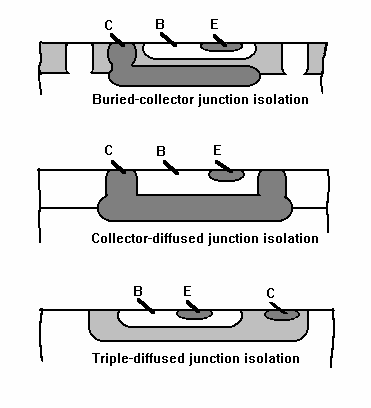
| 357 | Including epitaxial semiconductor layer formation: |
| This subclass is indented under subclass 356. Process for making a junction isolated bipolar transistor utilizing the formation of an epitaxial semiconductor layer. | |
| 358 | Up diffusion of dopant from substrate into epitaxial layer: |
| This subclass is indented under subclass 357. Process including a step of diffusing a dopant from the semiconductor substrate into the epitaxial layer form thereupon. | |
| 359 | Dielectric isolation formed by grooving and refilling with dielectrical material: |
| This subclass is indented under subclass 353. Process for making a bipolar transistor involving the formation of a recess in the semiconductor followed by the refilling of the recess with an insulative material. | |
| 360 | With epitaxial semiconductor formation in groove: |
| This subclass is indented under subclass 359. Process for making a bipolar transistor additionally involving the epitaxial deposition of a semiconductor material in the groove. | |
| 361 | Including deposition of polysilicon or noninsulative material into groove: |
| This subclass is indented under subclass 359. Process for making a bipolar transistor wherein a noninsulative material is deposited into the groove in addition to the insulative material. | |
| 362 | Recessed oxide by localized oxidation (i.e., LOCOS): |
| This subclass is indented under subclass 353. Process for making a bipolar transistor including the step of oxidizing a portion of a semiconductive material to form an embedded oxide (i.e., field oxide) therein which forms the periphery of a semiconductive region utilized for the formation of the bipolar transistor. | |
| 363 | With epitaxial semiconductor layer formation: |
| This subclass is indented under subclass 362. Process for making a bipolar transistor utilizing in addition to the recessed oxide the formation of an epitaxial semiconductor layer. | |
| 364 | Self-aligned: |
| This subclass is indented under subclass 309. Process wherein a previously formed device feature is utilized to make device regions in the desired registration to the previously formed feature. | |
| 365 | Forming active region from adjacent doped polycrystalline or amorphous semiconductor: |
| This subclass is indented under subclass 364. Process having an active region (e.g., base, emitter, or collector) formed of polycrystalline or amorphous semiconductor. | |
| 366 | Having sidewall: |
| This subclass is indented under subclass 365. Process including forming dielectric isolation on the sidewall of the base region to separate the base and collector regions. | |
| 367 | Including conductive component: |
| This subclass is indented under subclass 366. Process wherein the sidewall is a combination of conductive and insulative components. | |
| 368 | Simultaneously outdiffusing plural dopants from polysilicon or amorphous semiconductor: |
| This subclass is indented under subclass 365. Process including the simultaneous outdiffusing of electrically active dopants from the polysilicon or amorphous active region. | |
| 369 | Dopant implantation or diffusion: |
| This subclass is indented under subclass 364. Process having a step of implanting or diffusing an electrically active dopant species into a semiconductive region of the substrate. | |
| 370 | Forming buried region (e.g., implanting through insulating layer, etc.): |
| This subclass is indented under subclass 369. Process wherein the dopant is implanted or diffused through an insulating layer. | |
| 371 | Simultaneous introduction of plural dopants: |
| This subclass is indented under subclass 369. Process involving the concurrent introduction of multiple dopant species into one or more semiconductive regions of the substrate. | |
| 372 | Plural doping steps: |
| This subclass is indented under subclass 369. Process having multiple steps of doping semiconductive regions of the substrate. | |
| 373 | Multiple ion implantation steps: |
| This subclass is indented under subclass 372. Process wherein the plural doping steps are affected by implanting electrically active dopant ions into semiconductive regions of the substrate. | |
| 374 | Using same conductivity-type dopant: |
| This subclass is indented under subclass 373. Process wherein the same conductivity-type electrically active dopant ion is introduced using plural ion implantation steps. | |
| 375 | Forming partially overlapping regions: |
| This subclass is indented under subclass 372. Process wherein the plural doping steps are affected upon localized areas which lap over each other in part. | |
| 376 | Single dopant forming regions of different depth or concentrations: |
| This subclass is indented under subclass 372. Process wherein the plural doping steps form regions which differ in amount of impurity or the distance the impurity has to travel inwardly from the surface. | |
| 377 | Through same mask opening: |
| This subclass is indented under subclass 372. Process wherein plural doping steps are affected through the same opening in a dopant masking layer. | |
| 378 | Radiation or energy treatment modifying properties of semiconductor regions of substrate (e.g., thermal, corpuscular, electromagnetic, etc.): | ||
| This subclass is indented under subclass 309. Process for making a bipolar transistor having a step of
irradiating the semiconductor substrate to alter the electrical
properties of semiconductive regions thereof.
SEE OR SEARCH THIS CLASS, SUBCLASS:
| |||
| 379 | VOLTAGE VARIABLE CAPACITANCE DEVICE MANUFACTURE (E.G., VARACTOR, ETC.): | ||||||
| This subclass is indented under the class definition. Process for making an active solid-state device
wherein the device changes its capacitance depending on the amount
of voltage applied thereto.
SEE OR SEARCH CLASS:
| |||||||
| 380 | AVALANCHE DIODE MANUFACTURE (E.G., IMPATT, TRAPPAT, ETC.): | ||||||
This subclass is indented under the class definition. Process for making a device which is configured to operate
in a manner in which an external voltage is applied in the reverse-conducting
direction of the semiconductor device junction with sufficient magnitude
to cause the potential barrier at the junction to breakdown due
to electrons or holes gaining sufficient speed to dislodge valence
electrons and thus create more hole-electron current carriers resulting
in a sudden change from high dynamic electrical resistance to very
low dynamic resistance.
SEE OR SEARCH THIS CLASS, SUBCLASS:
SEE OR SEARCH CLASS:
| |||||||
| 381 | MAKING PASSIVE DEVICE (E.G., RESISTOR, CAPACITOR, ETC.): | ||||||||||||||||||||||
This subclass is indented under the class definition. Process for making an electrical device or component utilizing
a semiconductor substrate in which charge carriers do not change their
energy levels and that does not provide rectification, amplification, or
switching, but which does react to voltage and current
input.
SEE OR SEARCH THIS CLASS, SUBCLASS:
SEE OR SEARCH CLASS:
| |||||||||||||||||||||||
| 382 | Resistor: | ||||||||
| This subclass is indented under subclass 381. Process involving the manufacture of an electrically resistive
element utilizing a semiconductor substrate.
SEE OR SEARCH THIS CLASS, SUBCLASS:
| |||||||||
| 383 | Lightly doped junction isolated resistor: |
| This subclass is indented under subclass 382. Process wherein the resistive element is in the form of a lightly doped layer of one conductivity type located in a region of opposite conductivity type, such that the pn junction between the resistor region and its containing opposite conductivity-type region serves to electrically isolate the resistor. | |
| 384 | Deposited thin film resistor: | ||
| This subclass is indented under subclass 382. Process wherein the resistor is formed by the deposition
of resistive material upon the semiconductor substrate.
SEE OR SEARCH CLASS:
| |||
| 385 | Altering resistivity of conductor: |
| This subclass is indented under subclass 384. Process wherein the electrical resistivity of a conductive material (i.e., metallization) is altered subsequent to deposition. | |
| 386 | Trench capacitor: |
| This subclass is indented under subclass 381. Process for making a capacitor located in a groove in a semiconductive substrate. | |
| 387 | Having stacked capacitor structure (e.g., stacked trench, buried stacked capacitor, etc.): |
| This subclass is indented under subclass 386. Process wherein the trench capacitor contains a number of capacitor plate regions aligned vertically above each other. | |
| 388 | With epitaxial layer formed over the trench: |
| This subclass is indented under subclass 386. Process for making a trench capacitor including a step of forming an epitaxial semiconductive layer over the trench region. | |
| 389 | Including doping of trench surfaces: | ||
| This subclass is indented under subclass 386. Process for making a trench capacitor having a step of introducing
electrically active dopant species into a surface (i.e., sidewall
or bottom) of the trench in which the capacitor is located.
SEE OR SEARCH THIS CLASS, SUBCLASS:
| |||
| 390 | Multiple doping steps: |
| This subclass is indented under subclass 389. Process for making a trench capacitor utilizing plural doping steps. | |
| 391 | Including isolating means formed in trench: |
| This subclass is indented under subclass 389. Process for making a trench capacitor having structure functioning as electrical isolation formed in the trench bottom. | |
| 392 | Doping by outdiffusion from a dopant source layer (e.g., doped oxide): |
| This subclass is indented under subclass 389. Process for making a trench capacitor wherein the trench surfaces are doped via outdiffusion from a doped source layer. | |
| 393 | Planar capacitor: |
| This subclass is indented under subclass 386. Process for making a capacitor wherein a generally planar region of a semiconductive substrate forms a first capacitor plate with a dielectric layer and a second capacitor plate formed thereupon. | |
| 394 | Including doping of semiconductive region: |
| This subclass is indented under subclass 393. Process for making a planar capacitor having a step of introducing electrically active dopant species into a semiconductive region of the substrate forming the first capacitor plate. | |
| 395 | Multiple doping steps: |
| This subclass is indented under subclass 394. Process for making a planar capacitor utilizing plural steps of incorporating electrically active dopant species into a semiconductive region of the substrate forming the first capacitor plate. | |
| 396 | Stacked capacitor: |
| This subclass is indented under subclass 386. Process for making a capacitor containing a number of capacitor plate and dielectric layers deposited successively one atop another. | |
| 397 | Including selectively removing material to undercut and expose storage node layer: | ||
This subclass is indented under subclass 396. Process for making a stacked capacitor having a step of
selectively removing material to undercut and expose the capacitor
electrode which serves as the storage node layer.
| |||
| 398 | Including texturizing storage node layer: | ||
This subclass is indented under subclass 396. Process for making a stacked capacitor having a step of
roughening the surface of the capacitor plate which serves as the
storage node layer.
| |||
| 399 | Having contacts formed by selective growth or deposition: |
| This subclass is indented under subclass 396. Process for making a stacked capacitor wherein electrical contacts are formed by selective growth or deposition of conductive material onto the substrate. | |
| 400 | FORMATION OF ELECTRICALLY ISOLATED LATERAL SEMICONDUCTIVE STRUCTURE: | ||||||||||||||||||||
This subclass is indented under the class definition. Process for making partial or total electrical isolation
means serving to minimize electrical current flow between laterally
adjoining semiconductive regions of the substrate.
SEE OR SEARCH THIS CLASS, SUBCLASS:
SEE OR SEARCH CLASS:
| |||||||||||||||||||||
| 401 | Having substrate registration feature (e.g., alignment mark): |
| This subclass is indented under subclass 400. Process wherein the process of forming electrical isolation utilizes an alignment feature formed on the semiconductive substrate or forms an alignment feature for subsequent use. | |
| 402 | And gettering of substrate: |
| This subclass is indented under subclass 400. Process for making laterally spaced electrically isolated semiconductor regions having a step of gettering a semiconductor substrate. | |
| 403 | Having semi-insulating component: |
| This subclass is indented under subclass 400. Process for making laterally spaced electrically isolated semiconductor regions wherein a high resistivity semiconductive component serves to electrically isolate, at least in part, the laterally spaced regions. | |
| 404 | Total dielectric isolation: | ||||||
| This subclass is indented under subclass 400. Process for making laterally spaced electrically isolated
semiconductor regions wherein the semiconductive regions are fully
electrically isolated by dielectric insulative material.
SEE OR SEARCH THIS CLASS, SUBCLASS:
| |||||||
| 405 | And separate partially isolated semiconductor regions: |
| This subclass is indented under subclass 404. Process for making a total dielectric isolation semiconductor structure additionally having laterally spaced semiconductor regions at least one of which is fully electrically isolated from other laterally spaced semiconductive regions and at least one other region which is partially electrically isolated from another laterally spaced semiconductive region. | |
| 406 | Bonding of plural semiconductive substrates: | ||
| This subclass is indented under subclass 404. Process for making a total dielectric isolation semiconductor
structure including a step of joining plural semiconductive substrates together
into a coherent monolith, such as by thermal treatment.
SEE OR SEARCH THIS CLASS, SUBCLASS:
| |||
| 407 | Nondopant implantation: | ||
This subclass is indented under subclass 404. Process for making a total dielectric isolation semiconductor
structure including a step of ion implantation of a nonelectrically
active impurity into a semiconductive region of the substrate.
| |||
| 408 | With electrolytic treatment step: |
| This subclass is indented under subclass 404. Process for making a total dielectric isolation semiconductor structure including a step of electrochemical treatment of the semiconductor substrate (i.e., such as to affect etching or coating action thereupon). | |
| 409 | Porous semiconductor formation: |
| This subclass is indented under subclass 408. Process wherein the electrolytic treatment results in the formation of a porous semiconductor component. | |
| 410 | Encroachment of separate locally oxidized regions: |
| This subclass is indented under subclass 404. Process for making a total dielectric isolation semiconductor structure including a step of oxidation of adjacent semiconductive regions whereby the oxidized regions acquire a touching relationship. | |
| 411 | Air isolation (e.g., beam lead supported semiconductor islands, etc.): | ||||||
| This subclass is indented under subclass 404. Process for making a total dielectric isolation structure
wherein the resulting structure has islands of semiconductor material
supported by beam leads and separated by air.
SEE OR SEARCH THIS CLASS, SUBCLASS:
SEE OR SEARCH CLASS:
| |||||||
| 412 | Semiconductor islands formed upon insulating substrate or layer (e.g., mesa isolation, etc.): |
| This subclass is indented under subclass 411. Process for making a total dielectric isolation semiconductor structure wherein laterally spaced semiconductor islands are formed upon an insulative substrate or layer. | |
| 413 | With epitaxial semiconductor formation: |
| This subclass is indented under subclass 404. Process for making a total dielectric isolation semiconductor structure having a step of epitaxially depositing a semiconductive layer onto the substrate. | |
| 414 | Isolation by PN junction only: |
| This subclass is indented under subclass 400. Process whereby the laterally spaced regions of the semiconductor substrate are electrically isolated solely through the use of properly biased PN junctions. | |
| 415 | Thermomigration: |
| This subclass is indented under subclass 414. Process for making junction isolated laterally spaced semiconductor regions having a step of dopant migration under the influence of a temperature gradient. | |
| 416 | With epitaxial semiconductor formation: |
| This subclass is indented under subclass 414. Process for making junction isolated laterally spaced semiconductor regions having a step of epitaxially depositing a semiconductor layer. | |
| 417 | And simultaneous polycrystalline growth: |
| This subclass is indented under subclass 416. Process for making junction isolated laterally spaced semiconductor regions in which polycrystalline semiconductive regions are deposited simultaneously with the epitaxial deposition. | |
| 418 | Dopant addition: |
| This subclass is indented under subclass 416. Process for making junction isolated laterally spaced semiconductor regions including a step of introducing an electrically active dopant species into semiconductive regions of the substrate. | |
| 419 | Plural doping steps: |
| This subclass is indented under subclass 418. Process for making junction isolated laterally spaced semiconductor regions including multiple steps of introducing an electrically active dopant species into semiconductive regions of the substrate. | |
| 420 | Plural doping steps: |
| This subclass is indented under subclass 414. Process for making an junction isolated laterally spaced semiconductor regions including multiple steps of introducing an electrically active dopant species into semiconductive regions of the substrate. | |
| 421 | Having air-gap dielectric (e.g., groove, etc.): | ||
| This subclass is indented under subclass 400. Process for making an electrically isolated laterally spaced
semiconductor structure resulting in laterally spaced semiconductive
regions separated at least in part by a recessed air-gap
feature relative to the surrounding surface (e.g., groove, trench, notch, etc.).
SEE OR SEARCH THIS CLASS, SUBCLASS:
| |||
| 422 | Enclosed cavity: |
| This subclass is indented under subclass 421. Process wherein the air-gap dielectric is in the form of an enclosed cavity or void between the laterally spaced semiconductive regions. | |
| 423 | Implanting to form insulator: | ||||
| This subclass is indented under subclass 400. Process for making an electrically isolated laterally spaced
semiconductor structure including a step of implanting a nonelectrically
active dopant species to form an insulative region which serves
to electrically isolate lateral semiconductive regions.
SEE OR SEARCH THIS CLASS, SUBCLASS:
| |||||
| 424 | Grooved and refilled with deposited dielectric material: |
| This subclass is indented under subclass 400. Process for making electrically isolated laterally spaced semiconductor regions including a step of forming a recess or trench in the semiconductive substrate and refilling the same with deposited insulative material. | |
| 425 | Combined with formation of recessed oxide by localized oxidation: | ||||
This subclass is indented under subclass 424. Process for making electrically isolated laterally spaced
semiconductor regions by grooving and refilling with insulative
material including the step of forming an embedded oxide by localized
oxidation (of semiconductor material).
SEE OR SEARCH THIS CLASS, SUBCLASS:
| |||||
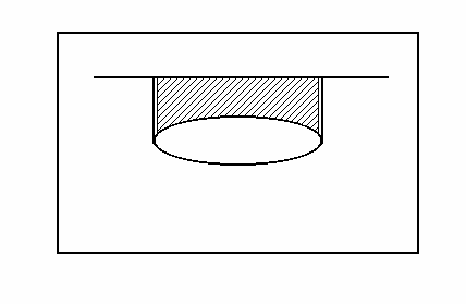
| 426 | Recessed oxide laterally extending from groove: |
| This subclass is indented under subclass 425. Process for making electrically isolated laterally spaced
semiconductor regions by grooving and refilling with insulative
material whereby the embedded oxidized region extends laterally from
the groove region.
| |
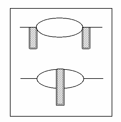
| 427 | Refilling multiple grooves of different widths or depths: |
| This subclass is indented under subclass 424. Process for making electrically isolated laterally spaced semiconductor regions by grooving and refilling with insulative material wherein grooves of differing widths or depths are filled with insulative material. | |
| 428 | Reflow of insulator: |
| This subclass is indented under subclass 427. Process for making electrically isolated laterally spaced semiconductor regions by grooving and refilling with insulative material including a step of redistributing insulative material by the viscous flow of the insulative material when exposed to high temperature. | |
| 429 | And epitaxial semiconductor formation in groove: |
| This subclass is indented under subclass 424. Process for making electrically isolated laterally spaced semiconductor regions by grooving and refilling with insulative material including a step of epitaxially depositing semiconductive material in the groove. | |
| 430 | And deposition of polysilicon or noninsulative material into groove: |
| This subclass is indented under subclass 424. Process for making electrically isolated laterally spaced semiconductor regions by grooving and refilling with insulative material wherein polysilicon or noninsulative material is deposited into the groove. | |
| 431 | Oxidation of deposited material: |
| This subclass is indented under subclass 430. Process for making electrically isolated laterally spaced semiconductor regions by grooving and refilling with insulative material including a step of oxidizing the polysilicon or noninsulative material deposited into the groove. | |
| 432 | Nonoxidized portions remaining in groove after oxidation: |
| This subclass is indented under subclass 431. Process for making electrically isolated laterally spaced semiconductor regions by grooving and refilling with insulative material wherein at least a portion of the polysilicon or noninsulative material deposited into the groove remains after the oxidation step. | |
| 433 | Dopant addition: |
| This subclass is indented under subclass 424. Process for making electrically isolated laterally spaced semiconductor regions by grooving and refilling with insulative material combined with a step of introducing an electrically active dopant species into a semiconductive region of the substrate. | |
| 434 | From doped insulator in groove: |
| This subclass is indented under subclass 433. Process for making electrically isolated laterally spaced semiconductor regions by grooving and refilling with insulative material wherein the semiconductor regions are doped from a doped insulator residing in the groove. | |
| 435 | Multiple insulative layers in groove: |
| This subclass is indented under subclass 424. Process for making electrically isolated laterally spaced semiconductor regions by grooving and refilling with plural insulative layers. | |
| 436 | Reflow of insulator: |
| This subclass is indented under subclass 435. Process for making electrically isolated laterally spaced semiconductor regions by grooving and refilling with insulative material including a step of redistributing insulative material by the viscous flow of the insulative material when exposed to high temperature. | |
| 437 | Conformal insulator formation: |
| This subclass is indented under subclass 435. Process for making electrically isolated laterally spaced semiconductor regions by grooving and refilling with insulative material including forming an insulative layer which follows the contour of the groove. | |
| 438 | Reflow of insulator: |
| This subclass is indented under subclass 424. Process for making electrically isolated laterally spaced semiconductor regions by grooving and refilling with insulative material including a step of redistributing insulative material by the viscous flow of the insulative material when exposed to high temperature. | |
| 439 | Recessed oxide by localized oxidation (i.e., LOCOS): |
| This subclass is indented under subclass 400. Process for making electrically isolated laterally spaced semiconductor regions including the step of oxidizing a portion of a semiconductive material to form an embedded oxide (e.g., field oxide) therein which isolates the laterally adjacent semiconductive regions. | |
| 440 | Including nondopant implantation: | ||||
This subclass is indented under subclass 439. Process including a step of ion implanting a nonelectrically
active impurity species into any region of
the semiconductor substrate.
SEE OR SEARCH THIS CLASS, SUBCLASS:
| |||||
| 441 | With electrolytic treatment step: |
| This subclass is indented under subclass 439. Process including a step of electrochemical treatment of the semiconductor substrate (e.g., such as to affect etching or coating action thereon). | |
| 442 | With epitaxial semiconductor layer formation: |
| This subclass is indented under subclass 439. Process including a step of epitaxially growing a single crystal semiconductor layer on the substrate. | |
| 443 | Etchback of recessed oxide: |
| This subclass is indented under subclass 439. Process having a step of thinning the formed recessed oxide by chemical etching action followed by an additional step of oxidizing a semiconductive region of the substrate. | |
| 444 | Preliminary etching of groove: | ||||
| This subclass is indented under subclass 439. Process including a preliminary step of etching a trench
into the semiconductive substrate followed by locally oxidizing
the trench surfaces to form the recessed oxide therein.
SEE OR SEARCH THIS CLASS, SUBCLASS:
| |||||
| 445 | Masking of groove sidewall: |
| This subclass is indented under subclass 444. Process utilizing a layer in contact with the groove sidewalls which serves as a protective covering during either an etching or oxidation step. | |
| 446 | Polysilicon containing sidewall: |
| This subclass is indented under subclass 445. Process utilizing a polysilicon containing component for masking the groove sidewalls. | |
| 447 | Dopant addition: |
| This subclass is indented under subclass 444. Process including a step of introducing an electrically active dopant species into semiconductive regions of the substrate. | |
| 448 | Utilizing oxidation mask having polysilicon component: |
| This subclass is indented under subclass 439. Process utilizing a layer in contact with the substrate having a polysilicon containing component which serves as a protective covering during the localized oxidation step. | |
| 449 | Dopant addition: |
| This subclass is indented under subclass 439. Process including a step of introducing an electrically active dopant species into semiconductive regions of the substrate. | |
| 450 | Implanting through recessed oxide: |
| This subclass is indented under subclass 449. Process wherein the dopant species is implanted through the recessed oxide into the semiconductive regions therebeneath. | |
| 451 | Plural doping steps: |
| This subclass is indented under subclass 449. Process utilizing multiple steps of doping semiconductive regions of the substrate. | |
| 452 | Plural oxidation steps to form recessed oxide: |
| This subclass is indented under subclass 439. Process having multiple steps of oxidizing the semiconductor substrate in the region of the recessed oxide. | |
| 453 | And electrical conductor formation (i.e., metallization): | ||||
This subclass is indented under subclass 439. Process including a step of making an electrically conductive
member integral to the semiconductive substrate.
SEE OR SEARCH THIS CLASS, SUBCLASS:
| |||||
| 454 | Field plate electrode: | ||
| This subclass is indented under subclass 400. Process having a step of forming an electrically conductive
structure formed on a major surface of the semiconductor substrate
for electrically separating laterally positioned device regions.
SEE OR SEARCH THIS CLASS, SUBCLASS:
| |||
| 455 | BONDING OF PLURAL SEMICONDUCTOR SUBSTRATES: | ||||||||||||||
This subclass is indented under the class definition. Process in which plural semiconductive substrates are joined
together into a coherent body, such as by thermal treatment.
SEE OR SEARCH THIS CLASS, SUBCLASS:
SEE OR SEARCH CLASS:
| |||||||||||||||
| 456 | Having enclosed cavity: | ||
| This subclass is indented under subclass 455. Process for joining plural semiconductive substrates into
an integral body resulting in a partially or wholly enclosed void
structure therein.
SEE OR SEARCH THIS CLASS, SUBCLASS:
| |||
| 457 | Warping of semiconductor substrate: |
| This subclass is indented under subclass 455. Process for joining plural semiconductive substrates into an integral body including a step of bending one or more of the semiconductor substrates to be joined. | |
| 458 | Subsequent separation into plural bodies (e.g., delaminating, dicing, etc.): | ||
| This subclass is indented under subclass 455. Process for joining plural semiconductive substrates into
an integral body having a step of dividing the integral body into
plural individual bodies subsequent to the joining operation.
SEE OR SEARCH CLASS:
| |||
| 459 | Thinning of semiconductor substrate: |
| This subclass is indented under subclass 455. Process for joining plural semiconductive substrates into an integral body having a step of reducing the thickness of at least one of the semiconductive substrates. | |
| 460 | SEMICONDUCTOR SUBSTRATE DICING: | ||||||||
| This subclass is indented under the class definition. Process including the step of separating the semiconductor
substrate into plural individual bodies (e.g., die, etc.) usually
by removal of material therefrom or by cleavage thereof.
SEE OR SEARCH THIS CLASS, SUBCLASS:
SEE OR SEARCH CLASS:
| |||||||||
| 461 | Beam lead formation: | ||||
| This subclass is indented under subclass 460. Process for separating a semiconductor substrate into plural
individual bodies wherein the resultant bodies possess electrical
leads which extend beyond the edges of the body (i.e., cantilevered).
SEE OR SEARCH THIS CLASS, SUBCLASS:
SEE OR SEARCH CLASS:
| |||||
| 462 | Having specified scribe region structure (e.g., alignment mark, plural grooves, etc.): | ||||
This subclass is indented under subclass 460. Process wherein the region of the semiconductor substrate
delineating the separating boundary between adjacent die possesses
a specified structure.
| |||||
| 463 | By electromagnetic irradiation (e.g., electron, laser, etc.): | ||
This subclass is indented under subclass 460. Process utilizing electromagnetic radiation for dividing
the semiconductor substrate into plural distinct bodies.
| |||
| 464 | With attachment to temporary support or carrier: | ||
| This subclass is indented under subclass 460. Process including a step of attaching the semiconductor
substrate to a temporary holder to facilitate the handling of the
substrate.
SEE OR SEARCH THIS CLASS, SUBCLASS:
| |||
| 465 | Having a perfecting coating: |
| This subclass is indented under subclass 460. Process including a step of coating the semiconductor substrate with a coating which enhances the dicing operation. | |
| 466 | DIRECT APPLICATION OF ELECTRICAL CURRENT: | ||||||||||||||||||||
This subclass is indented under the class definition. Process including the step having an electric current come
in direct contact with the semiconductor substrate (i.e., nonradiatively) to
treat the same.
SEE OR SEARCH THIS CLASS, SUBCLASS:
SEE OR SEARCH CLASS:
| |||||||||||||||||||||
| 467 | To alter conductivity of fuse or antifuse element: | ||||||
| This subclass is indented under subclass 466. Process involving the direct application of electrical current
to a fuse or antifuse portion of the semiconductor substrate to
alter the conductivity of same.
SEE OR SEARCH THIS CLASS, SUBCLASS:
| |||||||
| 468 | Electromigration: |
| This subclass is indented under subclass 466. Process involving the movement of atoms (usually dopant atoms) under the influence of an electric field. | |
| 469 | Utilizing pulsed current: |
| This subclass is indented under subclass 466. Process wherein the electrical current is presented in periodic surges. | |
| 470 | Fusion of semiconductor region: | ||||||
| This subclass is indented under subclass 466. Process wherein semiconductor regions of the substrate are
melted upon application of the electrical current.
SEE OR SEARCH THIS CLASS, SUBCLASS:
| |||||||
| 471 | GETTERING OF SUBSTRATE: | ||||||||||||||
This subclass is indented under the class definition. Process having a step of treating a semiconductor substrate
to reduce or remove deleterious defects (impurities, vacancies, dislocations,
etc.) therefrom.
SEE OR SEARCH THIS CLASS, SUBCLASS:
SEE OR SEARCH CLASS:
| |||||||||||||||
| 472 | By vibrating or impacting: | ||
| This subclass is indented under subclass 471. Process wherein a step of vibrating the semiconductive substrate
or striking the semiconductive substrate with solid material is
utilized to produce a gettering effect.
SEE OR SEARCH CLASS:
| |||
| 473 | By implanting or irradiating: |
| This subclass is indented under subclass 471. Process wherein a step of implanting or irradiating the semiconductive substrate is utilized to produce a gettering effect. | |
| 474 | Ionized radiation (e.g., corpuscular or plasma treatment, etc.): |
| This subclass is indented under subclass 473. Process wherein ionized radiation is applied to the semiconductor substrate to produce a gettering effect. | |
| 475 | Hydrogen plasma (i.e., hydrogenization): |
| This subclass is indented under subclass 474. Process wherein the radiation is a plasma containing ionized hydrogen (i.e., proton irradiation). | |
| 476 | By layers which are coated, contacted, or diffused: |
| This subclass is indented under subclass 471. Process wherein the substrate is exposed to a specified material by (a) depositing a layer of the material on the substrate, (b) physically contacting the substrate with the material, or (c) diffusing into the substrate a gettering species to form a gettering region in the substrate. | |
| 477 | By vapor phase surface reaction: |
| This subclass is indented under subclass 471. Process in which the substrate is treated with a reactive gas mixture which preferentially forms volatile compounds with the undesired impurities. | |
| 478 | FORMATION OF SEMICONDUCTIVE ACTIVE REGION ON ANY SUBSTRATE (E.G., FLUID GROWTH, DEPOSITION, ETC.): | ||||||||||||||||||
This subclass is indented under the class definition. Process for depositing onto any substrate single or multiple
layers of semiconductor material adapted to serve as an active device region,
the semiconductive material being deposited as amorphous, polycrystalline,
or single crystalline material.
SEE OR SEARCH THIS CLASS, SUBCLASS:
SEE OR SEARCH CLASS:
| |||||||||||||||||||
| 479 | On insulating substrate or layer: | ||
This subclass is indented under subclass 478. Process wherein the semiconductor layer is deposited onto
an electrically insulating substrate or layer.
| |||
| 480 | Including implantation of ion which reacts with semiconductor substrate to form insulating layer: | ||
| This subclass is indented under subclass 479. Process for the deposition of a semiconductor layer onto
an electrically insulating layer including implanting an ion which
reacts with the semiconductive regions of the substrate to form
an electrically insulating layer.
SEE OR SEARCH THIS CLASS, SUBCLASS:
| |||
| 481 | Utilizing epitaxial lateral overgrowth: |
| This subclass is indented under subclass 479. Process wherein the semiconductor material is deposited so as to overlay electrically insulative material and such that epitaxial growth occurs laterally from a crystal seeding region. | |
| 482 | Amorphous semiconductor: |
| This subclass is indented under subclass 478. Process wherein the deposited semiconductive material possesses no regular crystalline lattice. | |
| 483 | Compound semiconductor: |
| This subclass is indented under subclass 482. Process wherein the deposited amorphous semiconductor is a compound semiconductor. | |
| 484 | Running length (e.g., sheet, strip, etc.): | ||
| This subclass is indented under subclass 482. Process involving the fluid growth of an amorphous semiconductor
onto a substrate presented as a continuum of indeterminate length.
SEE OR SEARCH THIS CLASS, SUBCLASS:
| |||
| 485 | Deposition utilizing plasma (e.g., glow discharge, etc.): |
| This subclass is indented under subclass 482. Process utilizing a plasma or glow discharge during the deposition of the semiconductive material. | |
| 486 | And subsequent crystallization: | ||
| This subclass is indented under subclass 482. Process having a step of depositing an amorphous semiconductor
layer combined with the subsequent crystallization of the amorphous semiconductor
layer.
SEE OR SEARCH CLASS:
| |||
| 487 | Utilizing wave energy (e.g., laser, electron beam, etc.): |
| This subclass is indented under subclass 486. Process whereby the crystallization is affected by the application of a source of wave energy to the amorphous semiconductor. | |
| 488 | Polycrystalline semiconductor: | ||
| This subclass is indented under subclass 478. Process wherein the deposited semiconductive material is
polycrystalline (i.e., possesses multiple crystalline regions having
grain boundaries therebetween).
SEE OR SEARCH THIS CLASS, SUBCLASS:
| |||
| 489 | Simultaneous single crystal formation: |
| This subclass is indented under subclass 488. Process wherein both single and polycrystalline regions are simultaneously formed on the same substrate. | |
| 490 | Running length (e.g., sheet, strip, etc.): | ||
| This subclass is indented under subclass 488. Process involving the fluid growth of an indeterminate length
of amorphous semiconductor.
SEE OR SEARCH THIS CLASS, SUBCLASS:
| |||
| 491 | And subsequent doping of polycrystalline semiconductor: |
| This subclass is indented under subclass 488. Process having a subsequent step of incorporating an electrically active dopant species into the polycrystalline semiconductive material. | |
| 492 | Fluid growth step with preceding and subsequent diverse operation: |
| This subclass is indented under subclass 478. Process having a step of the fluid growth of a semiconductor active region combined with a preceding nonfluid growth step and a subsequent nonfluid growth step. | |
| 493 | Plural fluid growth steps with intervening diverse operation: | ||
| This subclass is indented under subclass 478. Process wherein multiple fluid growth steps having combined
therewith at least one step not perfecting to either prior or subsequent
growth steps and which step is preformed intermediate to the multiple
fluid growth steps.
SEE OR SEARCH CLASS:
| |||
| 494 | Differential etching: |
| This subclass is indented under subclass 493. Process where the differential etching of the substrate intermediate to the steps of fluid growth of semiconductive material is the diverse step. | |
| 495 | Doping of semiconductor: |
| This subclass is indented under subclass 493. Process wherein the incorporation of an electrically active dopant species into a semiconductive region of the substrate intermediate to the steps of fluid growth of semiconductive material is the diverse step. | |
| 496 | Coating of semiconductive substrate with nonsemiconductive material: |
| This subclass is indented under subclass 493. Process wherein the coating of a nonsemiconductive material intermediate to the steps of fluid growth of semiconductive material is the diverse operation. | |
| 497 | Fluid growth from liquid combined with preceding diverse operation: | ||
This subclass is indented under subclass 478. Process having a nonfluid growth operation which precedes
the fluid growth of semiconductive material from the liquid state
and is not merely perfecting thereto.
| |||
| 498 | Differential etching: |
| This subclass is indented under subclass 497. Process wherein the differential etching of the substrate prior to the fluid growth of semiconductive material from the liquid state is the diverse step. | |
| 499 | Doping of semiconductor: |
| This subclass is indented under subclass 497. Process wherein a semiconductive region of the substrate is incorporated with an electrically active dopant species prior to a step of fluid growth of semiconductive material from the liquid state. | |
| 500 | Fluid growth from liquid combined with subsequent diverse operation: | ||
This subclass is indented under subclass 478. Process having a nonfluid growth operation which is subsequent
to the fluid growth of semiconductive active region from the liquid state
and is not merely perfecting thereto.
| |||
| 501 | Doping of semiconductor: |
| This subclass is indented under subclass 500. Process wherein a semiconductive region of the substrate is incorporated with an electrically active dopant species subsequent to a step of fluid growth of semiconductive material from the liquid state. | |
| 502 | Heat treatment: |
| This subclass is indented under subclass 500. Process wherein the substrate having the deposited semiconductor active region thereon is heat treated following a step of fluid growth of semiconductive material from the liquid state. | |
| 503 | Fluid growth from gaseous state combined with preceding diverse operation: | ||
This subclass is indented under subclass 478. Process having a nonfluid growth operation which precedes
the fluid growth of semiconductive material from the vapor state
and is not merely perfecting thereto.
| |||
| 504 | Differential etching: |
| This subclass is indented under subclass 503. Process wherein the differential etching of the substrate prior to the fluid growth of semiconductive material from the gaseous state is the diverse step. | |
| 505 | Doping of semiconductor: |
| This subclass is indented under subclass 503. Process wherein a semiconductive region of the substrate is incorporated with an electrically active dopant species prior to a step of fluid growth of semiconductive material from the vapor or gaseous state. | |
| 506 | Ion implantation: |
| This subclass is indented under subclass 505. Process wherein the doping is by implantation of dopant ions into the semiconductor regions of the substrate. | |
| 507 | Fluid growth from gaseous state combined with subsequent diverse operation: | ||
This subclass is indented under subclass 478. Process having a nonfluid growth operation which is subsequent
to the fluid growth of semiconductive active region from the gaseous state
and is not merely perfecting thereto.
| |||
| 508 | Doping of semiconductor: |
| This subclass is indented under subclass 507. Process wherein a semiconductive region of the substrate is incorporated with an electrically active dopant species subsequent to a step of fluid growth of semiconductive material from the gaseous state. | |
| 509 | Heat treatment: |
| This subclass is indented under subclass 507. Process wherein the substrate having the deposited semiconductor active region thereon is heat treated following a step of fluid growth of semiconductive material from the gaseous state. | |
| 510 | INTRODUCTION OF CONDUCTIVITY MODIFYING DOPANT INTO SEMICONDUCTIVE MATERIAL: | ||||||||||||
| This subclass is indented under the class definition. Process involving the incorporation within a semiconductive
substrate of material referred to as dopants or dopant modifiers
or impurity functioning to alter the electrical characteristics
of semiconductive regions thereof.
SEE OR SEARCH THIS CLASS, SUBCLASS:
SEE OR SEARCH CLASS:
| |||||||||||||
| 511 | Ordering or disordering | ||||
| This subclass is indented under subclass 510. Process for making semiconductor regions of the substrate
ordered or disordered prior to, simultaneous with, or subsequent
to a step of doping semiconductor regions of the substrate.
SEE OR SEARCH THIS CLASS, SUBCLASS:
| |||||
| 512 | Involving nuclear transmutation doping: | ||
| This subclass is indented under subclass 510. Process for introducing a dopant into semiconductor regions
of the substrate having a combination of diverse steps in which
one step involves the conversion of an element into a dopant by
nuclear transmutation.
SEE OR SEARCH CLASS:
| |||
| 513 | Plasma (e.g., glow discharge, etc.): | ||||
| This subclass is indented under subclass 510. Process involving the use of a gaseous vapor of ions in
equilibrium or a vapor of ions in vacuum in nonequilibrium state
(i.e., a "cold plasma") to introduce a dopant
into the semiconductive material.
SEE OR SEARCH THIS CLASS, SUBCLASS:
SEE OR SEARCH CLASS:
| |||||
| 514 | Ion implantation of dopant into semiconductor region: | ||||||||||||||
This subclass is indented under subclass 510. Process involving penetration of the surface of the semiconductive
regions of the substrate with electrically active dopant species
possessing sufficient kinetic energy therefor, usually resulting
in the formation of a barrier layer rectifying junction within the
semiconductive regions.
SEE OR SEARCH THIS CLASS, SUBCLASS:
SEE OR SEARCH CLASS:
| |||||||||||||||
| 515 | Ionized molecules |
| This subclass is indented under subclass 514. Process involving the use of ionized molecules possessing sufficient kinetic energy to penetrate the semiconductive substrate with one or more of the elements of the molecule remaining in the semiconductive regions functioning as an electrically active dopant. | |
| 516 | Including charge neutralization: |
| This subclass is indented under subclass 514. Process including discharging electrical charges which would otherwise accumulate in the semiconductor substrate due to the implantation of electrically active dopant ions therein. | |
| 517 | Of semiconductor layer on insulating substrate or layer: |
| This subclass is indented under subclass 514. Process wherein the electrically active dopant ions are implanted into a semiconductor layer or portion thereof, the semiconductor layer residing on an insulating substrate or layer. | |
| 518 | Of compound semiconductor: |
| This subclass is indented under subclass 514. Process wherein the semiconductive region into which the electrically active dopant is implanted is a compound semiconductor. | |
| 519 | Including multiple implantation steps: |
| This subclass is indented under subclass 518. Process having plural steps of implanting ions, at least one step of which introduces an electrically active dopant ion, into a compound semiconductive substrate. | |
| 520 | Providing nondopant ion (e.g., proton, etc.): | ||
This subclass is indented under subclass 519. Process wherein a nonelectrically active impurity species
is implanted into a compound semiconductor region of the substrate
in conjunction with the prior, simultaneous, or subsequent implantation
of an electrically active dopant ion.
| |||
| 521 | Using same conductivity-type dopant: |
| This subclass is indented under subclass 519. Process wherein the multiple implantation steps introduce electrically active dopant ions of the same conductivity type into one or more regions of the compound semiconductor substrate. | |
| 522 | Including heat treatment: | ||
| This subclass is indented under subclass 518. Process including a step of heat treating the substrate
having compound semiconductive regions.
SEE OR SEARCH THIS CLASS, SUBCLASS:
| |||
| 523 | And contact formation (i.e., metallization): |
| This subclass is indented under subclass 518. Process including a step of making an electrical contact to a compound semiconductor region of the substrate. | |
| 524 | Into grooved semiconductor substrate region: | ||||||
| This subclass is indented under subclass 514. Process wherein the electrically active dopant is implanted
into a trench or recess formed in a semiconductor region of the
substrate.
SEE OR SEARCH THIS CLASS, SUBCLASS:
| |||||||
| 525 | Using oblique beam: | ||
| This subclass is indented under subclass 514. Process wherein the angle of the ion beam relative to the
major surface of the semiconductor substrate is other than 90 degrees.
SEE OR SEARCH THIS CLASS, SUBCLASS:
| |||
| 526 | Forming buried region: | ||
This subclass is indented under subclass 514. Process involving a step of producing a region implanted
with an electrically active dopant which is not in contact with
the free surface of the semiconductor substrate through which it was
implanted.
| |||
| 527 | Including multiple implantation steps: |
| This subclass is indented under subclass 514. Process having plural steps of implanting ions, at least one step of which introduces an electrically active dopant ion, into a semiconductive substrate. | |
| 528 | Providing nondopant ion (e.g., proton, etc.): | ||
This subclass is indented under subclass 527. Process wherein a nonelectrically active impurity species
is implanted into a semiconductor region of the substrate in conjunction
with the prior, simultaneous, or subsequent implantation of an electrically
active dopant species.
| |||
| 529 | Using same conductivity-type dopant: |
| This subclass is indented under subclass 527. Process wherein the multiple implantation steps introduce electrically active dopant ions of the same conductivity type into one or more regions of the semiconductor substrate. | |
| 530 | Including heat treatment: | ||
| This subclass is indented under subclass 514. Process including a step of heat treating the semiconductive
substrate.
SEE OR SEARCH THIS CLASS, SUBCLASS:
| |||
| 531 | Using shadow mask: |
| This subclass is indented under subclass 514. Process involving the use of a spaced templet positioned with respect to the ion source and the semiconductor substrate in such a manner as to allow the electrically active dopant ions to impinge only a portion of the semiconductor substrate. | |
| 532 | Into polycrystalline region: |
| This subclass is indented under subclass 514. Process involving implanting electrically active dopant ions into polycrystalline semiconductive regions. | |
| 533 | And contact formation (i.e., metallization): |
| This subclass is indented under subclass 514. Process including a step of forming an electrical contact to a semiconductor region of the substrate. | |
| 534 | Rectifying contact (i.e., Schottky contact): |
| This subclass is indented under subclass 533. Process wherein the electrical contact is a rectifying contact. | |
| 535 | By application of corpuscular or electromagnetic radiation (e.g., electron, laser, etc.): | ||
This subclass is indented under subclass 510. Process having a step of applying corpuscular or electromagnetic
radiation to the semiconductor substrate to affect the incorporation
of an electrically active dopant therein.
| |||
| 536 | Recoil implantation: | ||
| This subclass is indented under subclass 535. Process involving the use of kinetic energy via the use
of applied corpuscular or electromagnetic radiation for introduction
of an electrically active dopant species to a semiconductive region
of the substrate whereby at least a portion of the kinetic energy
travels in other than a straight path (e.g., bounces back and forth).
SEE OR SEARCH CLASS:
| |||
| 537 | Fusing dopant with substrate (i.e., alloy junction): | ||||
This subclass is indented under subclass 510. Processes for incorporating an electrically active impurity
into a semiconductor material during an operation affecting the
partial melting of the substrate.
SEE OR SEARCH THIS CLASS, SUBCLASS:
| |||||
| 538 | Using additional material to improve wettability or flow characteristics (e.g., flux, etc.): |
| This subclass is indented under subclass 537. Processes including the incorporation of an agent to alter the melting and crystallization of the alloying operation. | |
| 539 | Application of pressure to material during fusion: |
| This subclass is indented under subclass 537. Processes wherein pressure is applied during the alloying operation. | |
| 540 | Including plural controlled heating or cooling steps or nonuniform heating: |
| This subclass is indented under subclass 537. Processes including regulated multiple cooling or heating operations, or nonuniform application of thermal energy to the semiconductor substrate during the alloying operation. | |
| 541 | Including diffusion after fusing step: |
| This subclass is indented under subclass 540. Processes including a step of solid-state diffusion subsequent to the alloying operation. | |
| 542 | Diffusing a dopant: |
| This subclass is indented under subclass 510. Processes for permeating an electrically active impurity in a semiconductive region of the substrate. | |
| 543 | To control carrier lifetime (i.e., deep level dopant): |
| This subclass is indented under subclass 542. Processes involving the introduction by diffusion of an impurity serving to form energy levels in the forbidden band of a semiconductor material that can act as traps for charge carriers (e.g., gold (Au), chromium (Cr), iron (Fe), nickel (Ni), etc.). | |
| 544 | To solid-state solubility concentration: |
| This subclass is indented under subclass 542. Processes involving the introduction by diffusion at a concentration level up to the limit at which precipitation out of solid solution begins to occur for the particular electrically active impurity in the semiconductive material. | |
| 545 | Forming partially overlapping regions: |
| This subclass is indented under subclass 542. Processes for permeating one or more electrically active impurities in localized areas which lap over each other only in part. | |
| 546 | Plural dopants in same region (e.g., through same mask opening, etc.): |
| This subclass is indented under subclass 542. Processes for applying multiply electrically active impurities in the same area. | |
| 547 | Simultaneously: |
| This subclass is indented under subclass 546. Processes wherein the multiple electrically active impurities are applied at the same time. | |
| 548 | Plural dopants simultaneously in plural regions: |
| This subclass is indented under subclass 542. Processes for permeating multiple electrically active impurities in multiple localized areas. | |
| 549 | Single dopant forming plural diverse regions (e.g., forming regions of different concentrations or of different depths, etc.): |
| This subclass is indented under subclass 542. Processes for permeating an electrically active impurity into multiple different localized areas which differ in the amount of impurity, the distance the impurity has to travel inwardly from the surface, or the like. | |
| 550 | Nonuniform heating: |
| This subclass is indented under subclass 542. Processes including the nonuniform application of thermal energy to the semiconductor substrate (e.g., heating distinct areas as opposed to heating the entire substrate, etc.). | |
| 551 | Using multiple layered mask: |
| This subclass is indented under subclass 542. Processes involving use of a mask composed of plural layers to retard the diffusion of an electrically active impurity. | |
| 552 | Having plural predetermined openings in master mask: | ||
This subclass is indented under subclass 551. Processes wherein the multiple layered diffusion mask contains
a multitude of desired openings.
| |||
| 553 | Using metal mask: |
| This subclass is indented under subclass 542. Processes involving use of a mask made from metal to retard the diffusion of an electrically active impurity. | |
| 554 | Outwardly: |
| This subclass is indented under subclass 542. Processes wherein the electrically active impurity moves from an internal location toward the major surface of the semiconductor substrate. | |
| 555 | Laterally under mask opening: |
| This subclass is indented under subclass 542. Processes wherein the direction of diffusion for the electrically active impurity includes a component parallel to the major surface of the masking layer. | |
| 556 | Edge diffusion by using edge portion of structure other than masking layer to mask: |
| This subclass is indented under subclass 542. Processes using an edge feature of the substrate other than a masking layer to retard the diffusion of the electrically active impurity. | |
| 557 | From melt: |
| This subclass is indented under subclass 542. Processes wherein the source of the electrically active impurity is molten material. | |
| 558 | From solid dopant source in contact with semiconductor region: |
| This subclass is indented under subclass 542. Processes wherein the electrically active impurity is produced by a solid substance which is in physical contact with the semiconductor region to be doped. | |
| 559 | Using capping layer over dopant source to prevent out-diffusion of dopant: |
| This subclass is indented under subclass 558. Processes including use of an overlying layer of material to prevent the diffusion of the electrically active impurity in the dopant source from moving therethrough. | |
| 560 | Plural diffusion stages: |
| This subclass is indented under subclass 558. Processes wherein the diffusion is carried out in multiple stages. | |
| 561 | Dopant source within trench or groove: |
| This subclass is indented under subclass 558. Processes wherein the solid dopant source material resides within the confines of a recessed region in the semiconductor substrate. | |
| 562 | Organic source: |
| This subclass is indented under subclass 558. Processes wherein the solid dopant source material is composed of other than inorganic matter. | |
| 563 | Glassy source or doped oxide: |
| This subclass is indented under subclass 558. Processes wherein the solid dopant source material is composed of a glass-type material or an oxide which has been doped. | |
| 564 | Polycrystalline semiconductor source: |
| This subclass is indented under subclass 558. Processes wherein the solid dopant source material is composed of a multicrystalline semiconductor (i.e., polysilicon). | |
| 565 | From vapor phase: |
| This subclass is indented under subclass 542. Processes wherein an electrically active impurity is produced using a gaseous substance as the dopant source material. | |
| 566 | Plural diffusion stages: |
| This subclass is indented under subclass 565. Processes wherein the diffusion is carried out in multiple stages. | |
| 567 | Solid source in operative relation with semiconductor region: |
| This subclass is indented under subclass 565. Processes wherein the dopant source material originates from a solid source in close proximity to the semiconductor region to be doped. | |
| 568 | In capsule-type enclosure: |
| This subclass is indented under subclass 567. Processes carried out in a small containerlike apparatus. | |
| 569 | Into compound semiconductor region: |
| This subclass is indented under subclass 565. Process wherein an electrically active dopant is diffused into a compound semiconductor. | |
| 570 | FORMING SCHOTTKY JUNCTION (I.E., SEMICONDUCTOR-CONDUCTOR RECTIFYING JUNCTION CONTACT): | ||||||||
| This subclass is indented under the class definition. Processes for making a metal-to-semiconductor interface
that exhibits a nonlinear impedance.
SEE OR SEARCH THIS CLASS, SUBCLASS:
SEE OR SEARCH CLASS:
| |||||||||
| 571 | Combined with formation of ohmic contact to semiconductor region: |
| This subclass is indented under subclass 570. Processes additionally having a method for the formation of an ohmic contact to a semiconductor region. | |
| 572 | Compound semiconductor: |
| This subclass is indented under subclass 570. Processes wherein the rectifying contact is formed on a compound semiconductor. | |
| 573 | Multilayer electrode: | ||
| This subclass is indented under subclass 572. Processes wherein the contact is composed of plural layers.
SEE OR SEARCH THIS CLASS, SUBCLASS:
| |||
| 574 | T-shaped electrode: |
| This subclass is indented under subclass 573. Processes wherein the contact is configured so as to possess a central conductive portion with adjacent conductive portions laterally extending therefrom. | |
| 575 | Using platinum group metal (i.e., platinum (Pt), palladium (Pd), rhodium (Rh), ruthenium (Ru), iridium (Ir), osmium (Os), or alloy thereof): |
| This subclass is indented under subclass 573. Processes for forming a contact using a platinum group metals (i.e., platinum (Pt), palladium (Pd), rhodium (Rh), ruthenium (Rh), iridium (Ir), osmium (Os), or alloy thereof). | |
| 576 | Into grooved or recessed semiconductor region: | ||
| This subclass is indented under subclass 572. Processes wherein the contact is formed in a recess in the
semiconductor substrate.
SEE OR SEARCH CLASS:
| |||
| 577 | Utilizing lift-off: |
| This subclass is indented under subclass 576. Processes including a step of material removal via a lift-off technique. | |
| 578 | Forming electrode of specified shape (e.g., slanted, etc.): |
| This subclass is indented under subclass 576. Processes wherein the contact possesses a specified shape. | |
| 579 | T-shaped electrode: |
| This subclass is indented under subclass 578. Processes wherein the contact is configured so as to possess a central conductive portion with adjacent conductive portions laterally extending therefrom. | |
| 580 | Using platinum group metal (i.e., platinum (Pt), palladium (Pd), rhodium (Rh), ruthenium (Ru), iridium (Ir), osmium (Os), or alloy thereof): |
| This subclass is indented under subclass 570. Processes for forming a contact using a platinum group metals (i.e., platinum (Pt), palladium (Pd), rhodium (Rh), ruthenium (Ru), iridium (Ir), osmium (Os), or alloy thereof). | |
| 581 | Silicide: |
| This subclass is indented under subclass 580. Processes for forming a contact using the chemical combination of silicon (Si) with one of the platinum group metals (i.e., platinum (Pt), palladium (Pd), rhodium (Rh), ruthenium (Ru), iridium (Ir), osmium (Os), or alloy thereof). | |
| 582 | Using refractory group metal (i.e., titanium (Ti), zirconium (Zr), hafnium (Hf), vanadium (V), niobium (Nb), tantalum (Ta), chromium (Cr), molybdenum (Mo), tungsten (W), or alloy thereof): |
| This subclass is indented under subclass 570. Processes for forming the contact using a refractory metal (i.e., titanium (Ti), zirconium (Zr), hafnium (Hf), vanadium (V), niobium (Nb), tantalum (Ta), chromium (Cr), molybdenum (Mo), tungsten (W), or alloy thereof). | |
| 583 | Silicide: |
| This subclass is indented under subclass 582. Processes for forming a contact using the chemical combination of silicon (Si) with one of the refractory group elements (i.e., titanium (Ti), zirconium (Zr), hafnium (Hf), vanadium (V), niobium (Nb), tantalum (Ta), chromium (Cr), molybdenum (Mo), tungsten (W), or alloy thereof). | |
| 584 | COATING WITH ELECTRICALLY OR THERMALLY CONDUCTIVE MATERIAL: | ||||||||||
This subclass is indented under the class definition. Processes having a step of depositing electrically or thermally
conductive material upon a semiconductive substrate.
SEE OR SEARCH THIS CLASS, SUBCLASS:
| |||||||||||
| 585 | Insulated gate formation: |
| This subclass is indented under subclass 584. Processes for forming an electrode which is electrically insulated from the adjoining semiconductor regions and which upon application of a voltage thereto exerts a change in electrical behavior in the adjoining semiconductor region. | |
| 586 | Combined with formation of ohmic contact to semiconductor region: |
| This subclass is indented under subclass 585. Processes having combined therewith the formation of an ohmic contact to a semiconductor region. | |
| 587 | Forming array of gate electrodes: | ||||||||||||
This subclass is indented under subclass 585. Process involving the deposition of electrically conductive
material resulting in the formation of a repeating geometrical arrangement
(e.g., multiple, adjacent electrically conductive elements) of
coplanar gate electrodes.
SEE OR SEARCH THIS CLASS, SUBCLASS:
SEE OR SEARCH CLASS:
| |||||||||||||
| 588 | Plural gate levels: | ||
| This subclass is indented under subclass 587. Processes wherein the array of insulated gate electrodes
reside on more than one level relative to the main surface of the
semiconductor substrate.
SEE OR SEARCH CLASS:
| |||
| 589 | Recessed into semiconductor substrate: |
| This subclass is indented under subclass 585. Processes wherein the insulated gate electrode is recessed below the main surface of the semiconductor substrate. | |
| 590 | Compound semiconductor: |
| This subclass is indented under subclass 585. Processes wherein the insulated gate is formed on a compound which is a semiconductor. | |
| 591 | Gate insulator structure constructed of plural layers or nonsilicon containing compound: |
| This subclass is indented under subclass 585. Processes wherein the gate insulator is a laminate of multiple dielectric layers or is a nonsilicon containing dielectric compound. | |
| 592 | Possessing plural conductive layers (e.g., polycide): |
| This subclass is indented under subclass 585. Processes wherein the electrode is a laminate of multiple conductive layers. | |
| 593 | Separated by insulator (i.e., floating gate): |
| This subclass is indented under subclass 592. Processes wherein an intervening dielectric layer separates the plural conductive layers. | |
| 594 | Tunnelling dielectric layer: |
| This subclass is indented under subclass 593. Processes wherein the intervening dielectric allows for the migration of charge carriers therethrough. | |
| 595 | Having sidewall structure: |
| This subclass is indented under subclass 585. Processes wherein the insulated gate electrode has material features formed along the electrode sidewall. | |
| 596 | Portion of sidewall structure is conductive: |
| This subclass is indented under subclass 595. Processes wherein a least a portion of the material features formed along the electrode sidewalls is electrically conductive. | |
| 597 | To form ohmic contact to semiconductive material: |
| This subclass is indented under subclass 584. Processes for depositing electrically conductive material which forms an indirect or direct ohmic contact to a semiconductive region. | |
| 598 | Selectively interconnecting (e.g., customization, wafer scale integration, etc.): | ||
| This subclass is indented under subclass 597. Processes wherein an array of devices is electrically interconnected
into a designated circuit arrangement.
SEE OR SEARCH THIS CLASS, SUBCLASS:
| |||
| 599 | With electrical circuit layout: |
| This subclass is indented under subclass 598. Processes including a step of designing the topological arrangement of electrical conductors between arrayed device components. | |
| 600 | Using structure alterable to conductive state (i.e., antifuse): |
| This subclass is indented under subclass 598. Processes for making an electrical interconnect structure which is alterable to a conductive state. | |
| 601 | Using structure alterable to nonconductive state (i.e., fuse): |
| This subclass is indented under subclass 598. Processes for making an electrical interconnect structure which is alterable to a nonconductive state. | |
| 602 | To compound semiconductor: |
| This subclass is indented under subclass 597. Processes wherein an ohmic contact is formed to a compound which is a semiconductor. | |
| 603 | II-VI compound semiconductor: |
| This subclass is indented under subclass 602. Processes wherein the compound semiconductor is composed of elements of Group II (i.e., zinc (Zn), cadmium (Cd), and mercury (Hg)) and Group VI (i.e., oxygen (O), sulfur (S), selenium (Se), and tellurium (Te)). | |
| 604 | III-V compound semiconductor: |
| This subclass is indented under subclass 602. Processes wherein the compound semiconductor is composed of elements of Group III (i.e., boron (B), aluminum (Al), gallium (Ga), and indium (In)) and Group V (i.e., nitrogen (N), phosphorus (P), arsenic (As), antimony (Sb), and bismuth (Bi)). | |
| 605 | Multilayer electrode: |
| This subclass is indented under subclass 604. Processes wherein the ohmic contact is composed of plural layers. | |
| 606 | Ga and As containing semiconductor: |
| This subclass is indented under subclass 604. Processes wherein the III-V compound semiconductor contains gallium (Ga) and arsenic (As). | |
| 607 | With epitaxial conductor formation: | ||
| This subclass is indented under subclass 597. Processes involving the formation of an epitaxial conductive
layer in ohmic electrical contact to a semiconductor region.
SEE OR SEARCH CLASS:
| |||
| 608 | Oxidic conductor (e.g., indium tin oxide, etc.): |
| This subclass is indented under subclass 597. Processes wherein the ohmic contact is formed of an electrically conductive oxide. | |
| 609 | Transparent conductor: |
| This subclass is indented under subclass 608. Processes wherein the oxidic conductor is transparent to electromagnetic radiation incident thereupon. | |
| 610 | Conductive macromolecular conductor (including metal powder filled composition): |
| This subclass is indented under subclass 597. Processes wherein the ohmic contact is formed of an electrically conductive macromolecular composition. | |
| 611 | Beam lead formation: | ||||
| This subclass is indented under subclass 597. Processes wherein the electrical contact leads extend beyond
the edge of the semiconductor substrate.
SEE OR SEARCH THIS CLASS, SUBCLASS:
| |||||
| 612 | Forming solder contact or bonding pad: |
| This subclass is indented under subclass 597. Processes for making an ohmic electrical contact to a semiconductor region which contact also serves as a solder contact or bonding pad. | |
| 613 | Bump electrode: |
| This subclass is indented under subclass 612. Processes wherein the electrical contact is in the shape of an abrupt protuberance elevated relative to the main surface of the substrate. | |
| 614 | Plural conductive layers: |
| This subclass is indented under subclass 613. Processes wherein the bump electrode is composed of multiple conductive layers. | |
| 615 | Including fusion of conductor: |
| This subclass is indented under subclass 613. Processes wherein at least a portion of the conductive material forming the bump electrode is molten during formation of the bump. | |
| 616 | By transcription from auxiliary substrate: |
| This subclass is indented under subclass 615. Processes wherein the bump electrode is formed by transcription of conductive material from an auxiliary substrate to the semiconductor substrate. | |
| 617 | By wire bonding: | ||||||
This subclass is indented under subclass 615. Processes wherein the bump electrode is formed by a process
which includes a step of utilizing a metallic wire to form the elevated structure.
SEE OR SEARCH CLASS:
| |||||||
| 618 | Contacting multiple semiconductive regions (i.e., interconnects): |
| This subclass is indented under subclass 597. Processes wherein the electrical contact is formed so as to make electrical contact to plural semiconductive regions | |
| 619 | Air bridge structure: |
| This subclass is indented under subclass 618. Processes wherein a portion of the electrical contact is suspended over the semiconductor substrate. | |
| 620 | Forming contacts of differing depths into semiconductor substrate: |
| This subclass is indented under subclass 618. Processes wherein at least one electrical contact is formed at a depth into the semiconductive substrate which differs from that of another electrical contact. | |
| 621 | Contacting diversely doped semiconductive regions (e.g., p-type and n-type regions, etc.): |
| This subclass is indented under subclass 618. Processes wherein at least one electrical contact is formed to a semiconductive region which is diversely doped (more heavily doped, oppositely doped, etc.) with respect to the semiconductive region contacted by another electrical contact. | |
| 622 | Multiple metal levels, separated by insulating layer (i.e., multiple level metallization): | ||
| This subclass is indented under subclass 618. Processes wherein there are plural levels of metal forming
electrical contact material, the levels being separated by intervening
dielectric material except at designated openings therethrough.
SEE OR SEARCH CLASS:
| |||
| 623 | Including organic insulating material between metal levels: | ||
This subclass is indented under subclass 622. Processes wherein the intervening dielectric is at least
partly composed of organic insulating material.
| |||
| 624 | Separating insulating layer is laminate or composite of plural insulating materials: |
| This subclass is indented under subclass 622. Processes wherein there is at least one separating insulator layer between different metal levels, which separating insulator layer is itself made up of plural sublayers or which separating layer is a composite such as a mixture of silicon oxide and silicon nitride. | |
| 625 | At least one metallization level formed of diverse conductive layers: |
| This subclass is indented under subclass 622. Processes wherein at least one of the metallization levels is composed of plural conductive layers of differing composition or electrical characteristics. | |
| 626 | Planarization: |
| This subclass is indented under subclass 625. Processes wherein at least one of the metallization levels or at least one separating insulating layer is leveled into a single plane at any stage in the process. | |
| 627 | At least one layer forms a diffusion barrier: |
| This subclass is indented under subclass 625. Processes wherein at least one of the diverse conductive layers forms a barrier to the migration of a contact material into the semiconductor or into another contact layer. | |
| 628 | Having adhesion promoting layer: |
| This subclass is indented under subclass 625. Processes wherein a material (e.g., layer, etc.) is utilized to promote adhesion of the electrical contact or lead to an adjacent surface. | |
| 629 | Diverse conductive layers limited to viahole/plug: |
| This subclass is indented under subclass 625. Processes wherein the diverse conductive layers of a metallization level are limited in lateral extent to the viahole or plug extending through an insulating layer. | |
| 630 | Silicide formation: |
| This subclass is indented under subclass 629. Processes wherein at least one of the diverse conductive layers is a compound of silicon and a metal. | |
| 631 | Having planarization step: |
| This subclass is indented under subclass 622. Processes wherein at least one of the metallization levels or at least one separating insulating layer is leveled into a single plane at any stage in the process. | |
| 632 | Utilizing reflow: |
| This subclass is indented under subclass 631. Processes wherein the planarization step is conducted by decreasing the viscosity of a layer and causing a leveling of the same by the viscous flow thereof. | |
| 633 | Simultaneously by chemical and mechanical means: | ||
| This subclass is indented under subclass 631. Processes wherein the planarization step is conducted by
the simultaneous chemical and mechanical material removal.
SEE OR SEARCH THIS CLASS, SUBCLASS:
| |||
| 634 | Utilizing etch-stop layer: |
| This subclass is indented under subclass 631. Processes wherein the planarization step is conducted utilizing an etch stop layer to limit the extent of a material removal operation. | |
| 635 | Insulator formed by reaction with conductor (e.g., oxidation, etc.): |
| This subclass is indented under subclass 622. Processes wherein an insulating layer is formed by the conversion of a conductive layer at least in part to an electrically insulative material. | |
| 636 | Including use of antireflective layer: |
| This subclass is indented under subclass 622. Processes including the use of an antireflection layer. | |
| 637 | With formation of opening (i.e., viahole) in insulative layer: |
| This subclass is indented under subclass 622. Processes including a step of forming an opening in the separating insulating layer. | |
| 638 | Having viaholes of diverse width: |
| This subclass is indented under subclass 637. Processes wherein at least one viahole is formed which is wider than at least one other viahole. | |
| 639 | Having viahole with sidewall component: |
| This subclass is indented under subclass 637. Processes wherein the viahole has an additional component formed along the sidewall thereof. | |
| 640 | Having viahole of tapered shape: |
| This subclass is indented under subclass 637. Processes wherein the viahole is formed so as to possess nonparallel sidewalls. | |
| 641 | Selective deposition: |
| This subclass is indented under subclass 622. Processes wherein a material is deposited selectively upon the semiconductor substrate. | |
| 642 | Diverse conductors: |
| This subclass is indented under subclass 618. Processes wherein the electrically conductive pathway contacting multiple semiconductive regions is composed of plural conductive layers of differing composition or electrical characteristics. | |
| 643 | At least one layer forms a diffusion barrier: |
| This subclass is indented under subclass 642. Processes wherein at least one of the diverse conductive layers forms a barrier to the diffusional migration of a contact material into the semiconductor or into another contact layer. | |
| 644 | Having adhesion promoting layer: |
| This subclass is indented under subclass 642. Processes wherein a material (e.g., layer, etc.) is utilized to promote adhesion of the electrical conductor to an adjacent surface. | |
| 645 | Having planarization step: |
| This subclass is indented under subclass 642. Processes wherein a material layer is leveled into a single plane at any stage in the process. | |
| 646 | Utilizing reflow: |
| This subclass is indented under subclass 645. Processes wherein the planarization step is conducted by decreasing the viscosity of a layer and causing a leveling of the same by the viscous flow thereof. | |
| 647 | Having electrically conductive polysilicon component: |
| This subclass is indented under subclass 642. Processes wherein one of the diverse conductive layers is polycrystalline silicon. | |
| 648 | Having refractory group metal (i.e., titanium (Ti), zirconium (Zr), hafnium (Hf), vanadium (V), niobium (Nb), tantalum (Ta), chromium (Cr), molybdenum (Mo), tungsten (W), or alloy thereof): |
| This subclass is indented under subclass 642. Processes for forming at least one layer of the diverse conductive layers using a refractory metal (i.e., titanium (Ti), zirconium (Zr), hafnium (Hf), vanadium (V), niobium (Nb), tantalum (Ta), chromium (Cr), molybdenum (Mo), tungsten (W), or alloy thereof). | |
| 649 | Silicide: |
| This subclass is indented under subclass 648. Processes for forming a conductive layer using the chemical combination of silicon (Si) with one of the refractory group elements (i.e., titanium (Ti), zirconium (Zr), hafnium (Hf), vanadium (V), niobium (Nb), tantalum (Ta), chromium (Cr), molybdenum (Mo), tungsten (W), or alloy thereof). | |
| 650 | Having noble group metal (i.e., silver (Ag), gold (Au), platinum (Pt), palladium (Pd), rhodium (Rh), ruthenium (Ru), iridium (Ir), osmium (Os), or alloy thereof): |
| This subclass is indented under subclass 642. Processes for forming at least one of the conductive layers using one of the noble group elements (e.g., silver (Ag), gold (Au), platinum (Pt), palladium (Pd), rhodium (Rh), ruthenium (Ru), iridium (Ir), osmium (Os), or alloy thereof). | |
| 651 | Silicide: |
| This subclass is indented under subclass 650. Processes for forming a contact using the chemical combination of silicon (Si) with one of the noble group elements (e.g., silver (Ag), gold (Au), platinum (Pt), palladium (Pd), rhodium (Rh), ruthenium (Ru), iridium (Ir), osmium (Os), or alloy thereof). | |
| 652 | Plural layered electrode or conductor: |
| This subclass is indented under subclass 597. Processes for making an ohmic contact to a semiconductor region involving the formation of multiple conductive layers of differing composition or electrical characteristics. | |
| 653 | At least one layer forms a diffusion barrier: |
| This subclass is indented under subclass 652. Processes wherein at least one of the diverse conductive layers forms a barrier to the diffusional migration of a contact material into the semiconductor or into another contact layer. | |
| 654 | Having adhesion promoting layer: |
| This subclass is indented under subclass 652. Processes wherein a material (e.g., layer, etc.) is utilized to promote adhesion of the electrical contact or lead to an adjacent surface. | |
| 655 | Silicide: |
| This subclass is indented under subclass 652. Processes wherein at least one of the diverse conductive layers is formed by the chemical combination of silicon (Si) with a metal atom. | |
| 656 | Having refractory group metal (i.e., titanium (Ti), zirconium (Zr), hafnium (Hf), vanadium (V), niobium (Nb), tantalum (Ta), chromium (Cr), molybdenum (Mo), tungsten (W), or alloy thereof): |
| This subclass is indented under subclass 652. Processes wherein at least one of the diverse conductive layers is formed using a refractory metal (i.e., titanium (Ti), zirconium (Zr), hafnium (Hf), vanadium (V), niobium (Nb), tantalum (Ta), chromium (Cr), molybdenum (Mo), or tungsten (W), or alloy thereof). | |
| 657 | Having electrically conductive polysilicon component: |
| This subclass is indented under subclass 652. Processes wherein one of the diverse conductive layers is polycrystalline silicon. | |
| 658 | Altering composition of conductor: | ||
This subclass is indented under subclass 597. Processes wherein the composition of the conductive material
which forms an ohmic contact to an adjacent semiconductive region
is altered (e.g., via implantation, diffusion, etc.)
| |||
| 659 | Implantation of ion into conductor: |
| This subclass is indented under subclass 658. Processes wherein an ion is implanted into the electrical conductor (e.g., to alter the composition thereof, etc.). | |
| 660 | Including heat treatment of conductive layer: | ||
| This subclass is indented under subclass 597. Processes wherein a thermal treatment is performed on the
electrically conductive layer (e.g., for modifying the electrical
properties thereof, etc.).
SEE OR SEARCH CLASS:
| |||
| 661 | Subsequent fusing conductive layer: |
| This subclass is indented under subclass 660. Processes wherein the conductive layer is melted subsequent to the deposition thereof. | |
| 662 | Utilizing laser: |
| This subclass is indented under subclass 661. Processes wherein the melting of the conductive layer is affected through the application of coherent radiant energy thereupon. | |
| 663 | Rapid thermal anneal: |
| This subclass is indented under subclass 660. Processes wherein the heat treatment is of sufficiently short time span so as to limit the thermal affects primarily to the electrically conductive layer. | |
| 664 | Forming silicide: |
| This subclass is indented under subclass 663. Processes wherein the rapid thermal anneal results in the formation of a single silicide layer by the reaction of a conductive layer and a silicon substrate region. | |
| 665 | Utilizing textured surface: |
| This subclass is indented under subclass 597. Processes wherein a surface is roughened at some stage in the process. | |
| 666 | Specified configuration of electrode or contact: | ||
| This subclass is indented under subclass 597. Processes wherein the ohmic electrode or contact has a specified
shape or configuration.
SEE OR SEARCH CLASS:
| |||
| 667 | Conductive feedthrough or through-hole in substrate: |
| This subclass is indented under subclass 666. Processes wherein the electrically conductive material is formed upon one surface of the semiconductor substrate and is able to make electrical contact with the opposing surface of the semiconductor substrate. | |
| 668 | Specified aspect ratio of conductor or viahole: |
| This subclass is indented under subclass 666. Processes wherein the width-to-depth ratio or width-to-height ratio of the electrical conductor or the viahole in which the same is to reside is given. | |
| 669 | And patterning of conductive layer: |
| This subclass is indented under subclass 597. Processes including the selective removal of portions of the conductive layer formed upon the semiconductor substrate. | |
| 670 | Utilizing lift-off: |
| This subclass is indented under subclass 669. Processes including a step of material removal via a lift-off technique. | |
| 671 | Utilizing multilayered mask: |
| This subclass is indented under subclass 669. Processes involving the use of a mask composed of plural layers. | |
| 672 | Plug formation (i.e., in viahole): |
| This subclass is indented under subclass 669. Processes wherein the patterning step results in the remaining conductive material being recessed below the top surface of the substrate. | |
| 673 | Tapered etching: |
| This subclass is indented under subclass 669. Processes wherein the patterning step is accomplished through a tapering etching step. | |
| 674 | Selective deposition of conductive layer: |
| This subclass is indented under subclass 597. Processes wherein the conductive material is deposited upon selected regions of the substrate. | |
| 675 | Plug formation (i.e., in viahole): |
| This subclass is indented under subclass 674. Processes wherein the selective deposition results in the deposited conductive material being recessed below the top surface of the substrate. | |
| 676 | Utilizing electromagnetic or wave energy: |
| This subclass is indented under subclass 674. Processes wherein the selective deposition is accomplished through the irradiation of localized regions of the substrate with electromagnetic or wave energy. | |
| 677 | Pretreatment of surface to enhance or retard deposition: |
| This subclass is indented under subclass 674. Processes including a step of treating the substrate surface preparatory to the selective deposition step to increase or decrease the deposition thereon. | |
| 678 | Electroless deposition of conductive layer: |
| This subclass is indented under subclass 597. Processes wherein the formation of the conductive layer is accomplished by immersion of the semiconductor substrate in a metallic salt solution and deposition therefrom without the use of electricity. | |
| 679 | Evaporative coating of conductive layer: |
| This subclass is indented under subclass 597. Processes wherein the formation of the conductive layer is accomplished through the evaporation of the conductive material from a source and the deposition of the same on the semiconductive substrate. | |
| 680 | Utilizing chemical vapor deposition (i.e., CVD): |
| This subclass is indented under subclass 597. Processes wherein the conductive material is deposited utilizing a vapor phase precursor which decomposes or reacts either in the gaseous phase or on a substrate. | |
| 681 | Of organo-metallic precursor (i.e., MOCVD): |
| This subclass is indented under subclass 680. Processes where the chemical vapor deposition process utilizes an organo-metallic compound. | |
| 682 | Silicide: |
| This subclass is indented under subclass 597. Processes wherein the conductive material is formed by the chemical combination of Silicon (Si) with a metal atom. | |
| 683 | Of refractory group metal (i.e., titanium (Ti), zirconium (Zr), hafnium (Hf), vanadium (V), niobium (Nb), tantalum (Ta), chromium (Cr), molybdenum (Mo), tungsten (W), or alloy thereof): |
| This subclass is indented under subclass 682. Processes for forming a contact using the chemical combination of silicon (Si) with one of the refractory group elements (i.e., titanium (Ti), zirconium (Zr), hafnium (Hf), vanadium (V), niobium (Nb), tantalum (Ta), chromium (Cr), molybdenum (Mo), tungsten (W), or alloy thereof). | |
| 684 | Electrically conductive polysilicon: |
| This subclass is indented under subclass 597. Processes for forming a contact using electrically conductive polycrystalline silicon. | |
| 685 | Refractory group metal (i.e., titanium (Ti), zirconium (Zr), hafnium (Hf), vanadium (V), niobium (Nb), tantalum (Ta), chromium (Cr), molybdenum (Mo), tungsten (W), or alloy thereof): |
| This subclass is indented under subclass 597. Processes for forming the contact using a refractory metal (i.e., titanium (Ti), zirconium (Zr), hafnium (Hf), vanadium (V), niobium (Nb), tantalum (Ta), chromium (Cr), molybdenum (Mo), tungsten (W), or alloy thereof). | |
| 686 | Noble group metal (i.e., silver (Ag), gold (Au), platinum (Pt), palladium (Pd), rhodium (Rh), ruthenium (Ru), iridium (Ir), osmium (Os), or alloy thereof): |
| This subclass is indented under subclass 597. Processes for forming a contact using one of the noble group elements (e.g., silver (Ag), gold(Au), platinum (Pt), palladium (Pd), rhodium (Rh), ruthenium (Ru), iridium (Ir), osmium (Os), or alloy thereof). | |
| 687 | Copper or copper alloy conductor: |
| This subclass is indented under subclass 597. Processes for forming a contact using copper (Cu) or an alloy thereof. | |
| 688 | Aluminum or aluminum alloy conductor: |
| This subclass is indented under subclass 597. Processes for forming a contact using aluminum (Al) or an alloy thereof. | |
| 689 | CHEMICAL ETCHING: | ||||||
| This subclass is indented under the class definition. Processes having a step of removing material from a semiconductor
substrate through the action of a chemical agent, wherein the intent
is to use the electrical properties of the semiconductor for at
least one of the purposes outlined in section I, C, of the class
definition for this class (438).
SEE OR SEARCH CLASS:
| |||||||
| 690 | Combined with the removal of material by nonchemical means (e.g., ablating, abrading, etc.): |
| This subclass is indented under subclass 689. Processes wherein the chemical removal is accompanied by the removal, either concurrently or consecutively, of material by nonchemical means. | |
| 691 | Combined mechanical and chemical material removal: |
| This subclass is indented under subclass 690. Processes wherein the nonchemical material removal is a mechanical (e.g., abrading, cutting, etc.) removal method. | |
| 692 | Simultaneous (e.g., chemical-mechanical polishing, etc.): |
| This subclass is indented under subclass 691. Processes wherein the chemical and mechanical material removal processes are concurrent. | |
| 693 | Utilizing particulate abradant: |
| This subclass is indented under subclass 692. Processes wherein the mechanical material removal is affected through the use of a particulate abrasive material. | |
| 694 | Combined with coating step: |
| This subclass is indented under subclass 689. Processes additionally having a step of depositing a material onto the semiconductive substrate. | |
| 695 | Simultaneous etching and coating: |
| This subclass is indented under subclass 694. Processes wherein the chemical etching and material deposition occur concurrently. | |
| 696 | Coating of sidewall: |
| This subclass is indented under subclass 694. Processes wherein the chemical etching and material deposition is affected so that only vertically disposed surfaces remain coated with the deposited material. | |
| 697 | Planarization by etching and coating: | ||
This subclass is indented under subclass 694. Processes wherein at least one surface of the semiconductor
substrate is leveled through a combination of chemical etching and
material deposition.
| |||
| 698 | Utilizing reflow: |
| This subclass is indented under subclass 697. Processes wherein the planarization method requires decreasing the viscosity of a layer residing on the substrate in order to fluidize the same. | |
| 699 | Plural coating steps: |
| This subclass is indented under subclass 697. Processes having multiple material deposition steps are utilized in the planarization of the surface. | |
| 700 | Formation of groove or trench: |
| This subclass is indented under subclass 694. Processes wherein at least one groove or trench is formed by a combination of chemical etching and material deposition. | |
| 701 | Tapered configuration: |
| This subclass is indented under subclass 700. Processes wherein the viahole or trench is formed so as to possess nonparallel sides. | |
| 702 | Plural coating steps: |
| This subclass is indented under subclass 700. Processes wherein the viahole or trench is formed by a process having multiple material deposition steps. | |
| 703 | Plural coating steps: |
| This subclass is indented under subclass 694. Processes having multiple material deposition steps. | |
| 704 | Having liquid and vapor etching steps: | ||
| This subclass is indented under subclass 689. Processes having a liquid (i.e., wet) chemical etching step
and a gaseous (i.e., dry) chemical etching step.
SEE OR SEARCH CLASS:
| |||
| 705 | Altering etchability of substrate region by compositional or crystalline modification: |
| This subclass is indented under subclass 689. Processes wherein the manner in which a semiconductor substrate is etched by a chemical etchant is altered by contacting the substrate prior to etching (a) with a material which alloys or diffuses into a substrate region or (b) by modifying the crystalline structure of a substrate region (e.g., amorphosizing, introducing dislocations, etc.). | |
| 706 | Vapor phase etching (i.e., dry etching): | ||||
This subclass is indented under subclass 689. Processes wherein the chemical etchant is in a gaseous state
when brought into contact with the semiconductive substrate.
SEE OR SEARCH THIS CLASS, SUBCLASS:
| |||||
| 707 | Utilizing electromagnetic or wave energy: |
| This subclass is indented under subclass 706. Processes wherein the vapor phase etching is conducted using irradiation of electromagnetic or wave energy. | |
| 708 | Photo-induced etching: |
| This subclass is indented under subclass 707. Processes involving the simultaneous irradiation of the substrate or adjoining space with infrared, visible, or ultraviolet radiation to induce the vapor phase etching of regions thereof. | |
| 709 | Photo-induced plasma etching: | ||
This subclass is indented under subclass 708. Processes wherein the photo-induced vapor phase etching
is accompanied with the excitation of the etchant into a plasma.
| |||
| 710 | By creating electric field (e.g., plasma, glow discharge, etc.): | ||||||
This subclass is indented under subclass 707. Processes involving the application of an electric field
to generate, modify, or control the vaporous reactant(s) used in
the chemical etching process.
SEE OR SEARCH CLASS:
| |||||||
| 711 | Utilizing multiple gas energizing means: |
| This subclass is indented under subclass 710. Processes wherein plural gas energizing means are utilized either simultaneously or consecutively to ionize the etching gas (e.g., RF discharge and a DC electron source, etc.) | |
| 712 | Reactive ion beam etching (i.e., RIBE): |
| This subclass is indented under subclass 710. Processes wherein the semiconductor substrate is mounted on the RF-powered electrode of the etching apparatus. | |
| 713 | Forming tapered profile (e.g., tapered etching, etc.): |
| This subclass is indented under subclass 710. Processes wherein the etchant removes material from the substrate resulting in a mesa or trench profile possessing nonparallel sides. | |
| 714 | Including change in etch influencing parameter (e.g., energizing power, etchant composition, temperature, etc.): |
| This subclass is indented under subclass 710. Processes wherein a parameter influencing material removal, such as energizing power, gas etchant composition, temperature, etc., is varied during the etching process. | |
| 715 | With substrate heating or cooling: |
| This subclass is indented under subclass 710. Processes including the temperature maintenance or modification of the semiconductor substrate during the etching thereof with the energized gas. | |
| 716 | With substrate handling (e.g., conveying, etc.): |
| This subclass is indented under subclass 710. Processes including the physical handling or manipulation of the semiconductor substrate in conjunction with the etching thereof. | |
| 717 | Utilizing multilayered mask: |
| This subclass is indented under subclass 710. Processes wherein selected regions of the semiconductor substrate are protected from the effects of the energized gas through use of a mask composed of plural layers. | |
| 718 | Compound semiconductor: |
| This subclass is indented under subclass 710. Processes wherein the material undergoing etching with the energized gas is a compound semiconductor. | |
| 719 | Silicon: |
| This subclass is indented under subclass 710. Processes wherein the material undergoing etching with the energized gas is silicon. | |
| 720 | Electrically conductive material (e.g., metal, conductive oxide, etc.): |
| This subclass is indented under subclass 710. Processes wherein the material undergoing etching with the energized gas is an electrically conductive material. | |
| 721 | Silicide: |
| This subclass is indented under subclass 720. Processes wherein the material undergoing etching with the energized gas is an electrically conductive compound of silicon and a metal atom. | |
| 722 | Metal oxide: |
| This subclass is indented under subclass 710. Processes wherein the material undergoing etching with the energized gas is a compound of a metal and oxygen. | |
| 723 | Silicon oxide or glass: |
| This subclass is indented under subclass 710. Processes wherein the material undergoing etching with the energized gas is a compound of silicon and oxygen or glass. | |
| 724 | Silicon nitride: |
| This subclass is indented under subclass 710. Process wherein the material undergoing etching with the energized gas is a compound of silicon and nitrogen. | |
| 725 | Organic material (e.g., resist, etc.): |
| This subclass is indented under subclass 710. Processes wherein the material undergoing etching with the energized gas is an organic material. | |
| 726 | Having microwave gas energizing: |
| This subclass is indented under subclass 710. Processes wherein the ionized etching gas is produced using a microwave source. | |
| 727 | Producing energized gas remotely located from substrate: |
| This subclass is indented under subclass 726. Processes wherein the etching gas is energized in a region spaced apart from the region in which the semiconductor substrate is located. | |
| 728 | Using magnet (e.g., electron cyclotron resonance, etc.): |
| This subclass is indented under subclass 727. Processes wherein the a magnet is utilized in producing or confining the energized gas. | |
| 729 | Using specified electrode/susceptor configuration (e.g., of multiple substrates using barrel-type susceptor, planar reactor configuration, etc.) to generate plasma: |
| This subclass is indented under subclass 710. Processes having a specified physical arrangement of electrode(s) and/or susceptor. | |
| 730 | Producing energized gas remotely located from substrate: |
| This subclass is indented under subclass 729. Processes wherein the etching gas is energized in a region spaced apart from the region in which the semiconductor substrate is located. | |
| 731 | Using intervening shield structure: |
| This subclass is indented under subclass 730. Processes wherein a blocking means is interposed between the region generating the energized gas and the region in which the semiconductor substrate resides. | |
| 732 | Using magnet (e.g., electron cyclotron resonance, etc.): |
| This subclass is indented under subclass 710. Processes wherein the a magnet is utilized in producing or confining the energized gas. | |
| 733 | Using orientation dependant etchant (i.e., anisotropic etchant): |
| This subclass is indented under subclass 706. Processes wherein the vapor phase etching of the semiconductor substrate is produced through the use of an etchant possessing varying etching rates upon varying crystallographic orientations. | |
| 734 | Sequential etching steps on a single layer: | ||
This subclass is indented under subclass 706. Processes wherein plural etching steps are carried out on
a single layer at different times.
| |||
| 735 | Differential etching of semiconductor substrate: |
| This subclass is indented under subclass 706. Processes directed to (a) contact only selected surface areas of the substrate with the etchant to remove a constituent part of the substrate at the selected surface areas only or (b) cause the substrate to be treated at different rates in different areas to produce a nonuniform surface. | |
| 736 | Utilizing multilayered mask: |
| This subclass is indented under subclass 735. Processes wherein selected regions of the semiconductor substrate are protected from the effects of the etching gas through use of a mask composed of plural layers. | |
| 737 | Substrate possessing multiple layers: |
| This subclass is indented under subclass 735. Processes wherein the semiconductor substrate undergoing etching possesses plural layers. | |
| 738 | Selectively etching substrate possessing multiple layers of differing etch characteristics: |
| This subclass is indented under subclass 737. Process involving the etching of a multilayered substrate, using a single etching step, where the process parameters used causes a difference of the etching rate or characteristic in at least two different layers of the substrate. | |
| 739 | Lateral etching of intermediate layer (i.e., undercutting): |
| This subclass is indented under subclass 738. Processes wherein an intermediate layer on the substrate is etched laterally to the major surface thereof. | |
| 740 | Utilizing etch stop layer: |
| This subclass is indented under subclass 738. Processes wherein the selective etching is effected through the use of a material resistant to the etchant. | |
| 741 | PN junction functions as etch stop: |
| This subclass is indented under subclass 740. Processes wherein the etch stop layer is a component of a PN junction. | |
| 742 | Electrically conductive material (e.g., metal, conductive oxide, etc.): |
| This subclass is indented under subclass 737. Processes wherein the material undergoing etching with the energized gas is an electrically conductive material. | |
| 743 | Silicon oxide or glass: |
| This subclass is indented under subclass 737. Processes wherein the material undergoing etching with the energized gas is a compound of silicon and oxygen or glass. | |
| 744 | Silicon nitride: |
| This subclass is indented under subclass 737. Process wherein the material undergoing etching with the energized gas is a compound of silicon and nitrogen. | |
| 745 | Liquid phase etching: |
| This subclass is indented under subclass 689. Processes wherein the chemical etchant is in a liquid state when brought into contact with the semiconductive substrate. | |
| 746 | Utilizing electromagnetic or wave energy: |
| This subclass is indented under subclass 745. Processes wherein the liquid phase etching is conducted using irradiation of electromagnetic or wave energy. | |
| 747 | With relative movement between substrate and confined pool of etchant: |
| This subclass is indented under subclass 745. Processes including the step of causing a relative motion between the semiconductor substrate being etched and the liquid phase etchant which is confined by a container. | |
| 748 | Projection of etchant against a moving substrate or controlling the angle or pattern of projected etchant: |
| This subclass is indented under subclass 745. Processes wherein the chemical etchant is sprayed upon the moving semiconductor substrate or sprayed upon the semiconductor substrate in a specific angle or pattern. | |
| 749 | Sequential application of etchant: |
| This subclass is indented under subclass 745. Processes wherein plural liquid phase etching steps are carried out on the semiconductor substrate in succession to one another. | |
| 750 | To same side of substrate: |
| This subclass is indented under subclass 749. Processes wherein the sequential liquid phase etching steps are carried out on the same major surface of the semiconductor substrate. | |
| 751 | Each etch step exposes surface of an adjacent layer: |
| This subclass is indented under subclass 750. Processes wherein a layer on the semiconductor substrate previously covered by a different layer is exposed by each liquid phase etching step. | |
| 752 | Germanium: |
| This subclass is indented under subclass 745. Processes wherein the material undergoing wet chemical etching is germanium (Ge). | |
| 753 | Silicon: |
| This subclass is indented under subclass 745. Processes wherein the material undergoing wet chemical etching is silicon (Si). | |
| 754 | Electrically conductive material (e.g., metal, conductive oxide, etc.): |
| This subclass is indented under subclass 745. Processes wherein the material undergoing wet chemical etching is an electrically conductive material. | |
| 755 | Silicide: |
| This subclass is indented under subclass 754. Processes wherein the material undergoing wet chemical etching is an electrically conductive compound of silicon and a metal atom. | |
| 756 | Silicon oxide: |
| This subclass is indented under subclass 745. Processes wherein the material undergoing wet chemical etching is a compound of silicon and oxygen. | |
| 757 | Silicon nitride: |
| This subclass is indented under subclass 745. Processes wherein the material undergoing wet chemical etching is a compound of silicon and nitrogen. | |
| 758 | COATING OF SUBSTRATE CONTAINING SEMICONDUCTOR REGION OR OF SEMICONDUCTOR SUBSTRATE: | ||||||||||||||||||||
This subclass is indented under the class definition. Processes for forming or applying a coating on a semiconductor
substrate, and wherein the intent is to use the electrical properties
of the semiconductor for at least one of the purposes outlined in
section I, B, of the Class 438 definition above.
SEE OR SEARCH THIS CLASS, SUBCLASS:
SEE OR SEARCH CLASS:
| |||||||||||||||||||||
| 759 | Combined with the removal of material by nonchemical means: |
| This subclass is indented under subclass 758. Processes having an additional step of removing material from the semiconductor substrate by nonchemical means (e.g., ablating, abrading, grinding, etc.) | |
| 760 | Utilizing reflow (e.g., planarization, etc.): |
| This subclass is indented under subclass 758. Processes wherein the coating step is combined with a step of decreasing the viscosity of the layer and causing a redistribution of the same by the viscous flow thereof. | |
| 761 | Multiple layers: |
| This subclass is indented under subclass 758. Processes wherein plural layers are formed upon the semiconductor substrate. | |
| 762 | At least one layer formed by reaction with substrate: |
| This subclass is indented under subclass 761. Processes wherein at least one of the layers is formed by reacting an external agent with a constituent of the substrate to form a compound thereof. | |
| 763 | Layers formed of diverse composition or by diverse coating processes: |
| This subclass is indented under subclass 761. Processes wherein the plural layers are formed utilizing different processes (e.g., thermal insulator with deposited insulator, etc.) or are of differing composition or physical characteristics (e.g., crystallinity, orientation, etc.). | |
| 764 | Formation of semi-insulative polycrystalline silicon: | ||||
| This subclass is indented under subclass 758. Processes involving the deposition of polycrystalline silicon
which possesses an electrical conductivity less than that typically
utilized for the formation of electrical devices.
SEE OR SEARCH THIS CLASS, SUBCLASS:
| |||||
| 765 | By reaction with substrate: |
| This subclass is indented under subclass 758. Processes wherein a coating layer is formed by reacting an external agent with a constituent of the substrate to form the coating thereupon. | |
| 766 | Implantation of ion (e.g., to form ion amorphousized region prior to selective oxidation, reacting with substrate to form insulative region, etc.): | ||||
| This subclass is indented under subclass 765. Processes having a step of implanting an ionized species
into a substrate region to form or facilitate formation of a reactive
coating layer.
SEE OR SEARCH THIS CLASS, SUBCLASS:
| |||||
| 767 | Compound semiconductor substrate: |
| This subclass is indented under subclass 765. Processes wherein the substrate region reacting with the external agent is a compound semiconductor. | |
| 768 | Reaction with conductive region: | ||
| This subclass is indented under subclass 765. Processes wherein the substrate region reacting with an
external agent is a conductive region or layer residing upon the
semiconductor substrate.
SEE OR SEARCH CLASS:
| |||
| 769 | Reaction with silicon semiconductive region (e.g., oxynitride formation, etc.): |
| This subclass is indented under subclass 765. Processes wherein the substrate region reacting with an external agent is a silicon semiconductor region. | |
| 770 | Oxidation: |
| This subclass is indented under subclass 769. Processes wherein the external agent supplies oxygen which reacts with the silicon substrate region to form a compound therewith. | |
| 771 | Using electromagnetic or wave energy: |
| This subclass is indented under subclass 770. Processes wherein the oxidation is conducted using irradiation of electromagnetic or wave energy. | |
| 772 | Microwave gas energizing: | ||||
This subclass is indented under subclass 771. Processes wherein the irradiation is of microwave frequency.
| |||||
| 773 | In atmosphere containing water vapor (i.e., wet oxidation): |
| This subclass is indented under subclass 770. Processes wherein the oxidation is carried out in an atmosphere containing water in vaporous form. | |
| 774 | In atmosphere containing halogen: |
| This subclass is indented under subclass 770. Processes wherein the oxidation is carried out in an atmosphere containing a halogen. | |
| 775 | Nitridation: |
| This subclass is indented under subclass 769. Processes wherein the external agent supplies nitrogen which reacts with the silicon substrate region to form a compound therewith. | |
| 776 | Using electromagnetic or wave energy: |
| This subclass is indented under subclass 775. Processes wherein the nitridation is conducted using irradiation of electromagnetic or wave energy. | |
| 777 | Microwave gas energizing: | ||||
This subclass is indented under subclass 776. Processes wherein the irradiation is of microwave frequency.
| |||||
| 778 | Insulative material deposited upon semiconductive substrate: |
| This subclass is indented under subclass 758. Processes wherein an insulative coating is formed upon the semiconductor substrate solely by the deposition of externally supplied material. | |
| 779 | Compound semiconductor substrate: |
| This subclass is indented under subclass 778. Processes wherein the substrate upon which is deposited the coating is a compound semiconductor. | |
| 780 | Depositing organic material (e.g., polymer, etc.): | ||
| This subclass is indented under subclass 778. Processes wherein the deposited material is at least partly
composed of organic material. An organic compound is one which
fulfills the requirements of the Class 260 definitions (i.e., has
a molecule characterized by two carbon atoms bonded together, one
atom of carbon being bonded to at least one atom of hydrogen or
a halogen, or one atom of carbon bonded to at least one atom of
nitrogen by a single or double bond, certain compounds such as HCN, CN-CN,
HNCO, HNCS, cyanogen halides, cyanamide, fulminic acid and metal
carbides, being exceptions to this rule).
SEE OR SEARCH THIS CLASS, SUBCLASS:
| |||
| 781 | Subsequent heating step modifying organic coating composition: |
| This subclass is indented under subclass 780. Processes including a subsequent thermal treatment step altering the chemical composition of the organic coating composition. | |
| 782 | With substrate handling during coating (e.g., immersion, spinning, etc.): |
| This subclass is indented under subclass 778. Processes wherein the semiconductor substrate is handled or manipulated in conjunction with the coating operation. | |
| 783 | Insulative material having impurity (e.g., for altering physical characteristics, etc.): |
| This subclass is indented under subclass 778. Processes wherein the deposited insulative material contains one or more impurities (e.g., for altering a physical characteristic such as etchability, for serving as a diffusion source for adjacent semiconductive regions of the substrate, etc.). | |
| 784 | Introduction simultaneous with deposition: |
| This subclass is indented under subclass 783. Processes wherein the impurity is introduced into the insulative material concurrently with the deposition step. | |
| 785 | Insulative material is compound of refractory group metal (i.e., titanium (Ti), zirconium (Zr), hafnium (Hf), vanadium (V), niobium (Nb), tantalum (Ta), chromium (Cr), molybdenum (Mo), tungsten (W), or alloy thereof): |
| This subclass is indented under subclass 778. Processes for forming an insulative compound using one of the refractory group elements (i.e., titanium (Ti), zirconium (Zr), hafnium (Hf), vanadium (V), niobium (Nb), tantalum (Ta), chromium (Cr), molybdenum (Mo), or tungsten (W)). | |
| 786 | Tertiary silicon containing compound formation (e.g., oxynitride formation, etc.): |
| This subclass is indented under subclass 778. Processes for forming an insulative compound of silicon and two other elements is deposited upon the semiconductor substrate. | |
| 787 | Silicon oxide formation: |
| This subclass is indented under subclass 778. Processes wherein the deposited insulative material is a compound of silicon and oxygen. | |
| 788 | Using electromagnetic or wave energy (e.g., photo-induced deposition, plasma, etc.): |
| This subclass is indented under subclass 787. Processes wherein the silicon oxide is deposited using irradiation of electromagnetic or wave energy. | |
| 789 | Organic reactant: |
| This subclass is indented under subclass 788. Processes wherein a reactant compound utilized during the deposition of silicon oxide is an organic material (e.g., organo-siloxane, etc.). | |
| 790 | Organic reactant: |
| This subclass is indented under subclass 787. Processes wherein a reactant compound utilized during the deposition of silicon oxide is an organic material (e.g., organo-siloxane, etc.). | |
| 791 | Silicon nitride formation: |
| This subclass is indented under subclass 778. Processes wherein the deposited material is a compound of silicon and nitrogen. | |
| 792 | Using electromagnetic or wave energy (e.g., photo-induced deposition, plasma, etc.): |
| This subclass is indented under subclass 791. Processes wherein the silicon nitride is deposited using irradiation of electromagnetic or wave energy. | |
| 793 | Organic reactant: |
| This subclass is indented under subclass 792. Processes wherein a reactant compound utilized during the deposition of silicon nitride is an organic material (e.g., organo-siloxane, etc.). | |
| 794 | Organic reactant: |
| This subclass is indented under subclass 791. Processes wherein a reactant compound utilized during the deposition of silicon nitride is an organic material (e.g., organo-siloxane, etc.). | |
| 795 | RADIATION OR ENERGY TREATMENT MODIFYING PROPERTIES OF SEMICONDUCTOR REGION OF SUBSTRATE (E.G., THERMAL, CORPUSCULAR, ELECTROMAGNETIC, ETC.): | ||||||||||||||
| This subclass is indented under the class definition. Process of radiating a semiconductor substrate with a form
of energy to change some characteristic thereof.
SEE OR SEARCH THIS CLASS, SUBCLASS:
SEE OR SEARCH CLASS:
| |||||||||||||||
| 796 | Compound semiconductor: |
| This subclass is indented under subclass 795. Process wherein the substrate being modified is a compound semiconductor. | |
| 797 | Ordering or disordering: | ||||
| This subclass is indented under subclass 796. Process wherein a compound semiconductive region is transformed
from an ordered state to a disordered state or vice versa.
SEE OR SEARCH THIS CLASS, SUBCLASS:
| |||||
| 798 | Ionized irradiation (e.g., corpuscular or plasma treatment, etc.): | ||||
| This subclass is indented under subclass 795. Process wherein ionized radiation is applied to the semiconductor
to modify the properties thereof.
SEE OR SEARCH THIS CLASS, SUBCLASS:
| |||||
| 799 | By differential heating: | ||
| This subclass is indented under subclass 795. Process involving the nonuniform heating of a semiconductive
substrate to modify the properties of semiconductor regions thereof.
SEE OR SEARCH CLASS:
| |||
| 800 | MISCELLANEOUS: |
| This subclass is indented under the class definition. Process not provided for above. | |
CROSS-REFERENCE ART COLLECTIONS
| 900 | BULK EFFECT DEVICE MAKING: |
| Art collection involving the construction of a semiconductor device whose electrical characteristics and electronic properties are exhibited throughout the entire body of the material, rather than in just a localized region thereof (e.g., the surface). | |
| 901 | CAPACITIVE JUNCTION: |
| Art collection involving the construction of a barrier layer junction possessing capacitive properties. | |
| 902 | CAPPING LAYER: |
| Art collection involving the use of an overlayer serving to separate and protect an underlying region or layer from the environment. | |
| 903 | CATALYST AIDED DEPOSITION: |
| Art collection involving the use of a catalyst to facilitate material deposition. | |
| 904 | CHARGE CARRIER LIFETIME CONTROL: |
| Art collection involving the control of the lifetime of charge carriers (i.e., electrons or holes) in the semiconductor. | |
| 905 | CLEANING OF REACTION CHAMBER: |
| Art collection involving cleaning an etch chamber. | |
| 906 | CLEANING OF WAFER AS INTERIM STEP: |
| Art collection involving cleaning a semiconductive wafer as a step between other processing steps. | |
| 907 | CONTINUOUS PROCESSING: |
| Art collection involving carrying out process steps in semiconductor manufacture in a continual manner. | |
| 908 | Utilizing cluster apparatus: |
| This subclass is indented under subclass 907. Art collection wherein the continuous processing is conducted in an apparatus having a plurality of processing chambers having associated handling means to move the semiconductor substrate therebetween. | |
| 909 | CONTROLLED ATMOSPHERE: |
| Art collection involving use of a regulated gaseous environment (e.g., inert gases, specifically proportioned mixtures, etc.). | |
| 910 | CONTROLLING CHARGING STATE AT SEMICONDUCTOR-INSULATOR INTERFACE: |
| Art collection involving adjusting the charge state where the semiconductor and insulator surfaces meet. | |
| 911 | DIFFERENTIAL OXIDATION AND ETCHING: |
| Art collection involving differential oxidation combined with an etching process. | |
| 912 | DISPLACING PN JUNCTION: |
| Art collection involving physical relocation of the P-N junction from its originally formed position. | |
| 913 | DIVERSE TREATMENTS PERFORMED IN UNITARY CHAMBER: |
| Art collection involving diverse treatments performed upon a semiconductor substrate which are affected in a single processing chamber. | |
| 914 | DOPING: |
| Art collection involving the doping of a semiconductor substrate with conductivity modifying impurities. | |
| 915 | Amphoteric doping: |
| Art collection under 914 involving use of a dopant capable of functioning as a P- or N-type conductivity modifier depending on process conditions. | |
| 916 | Autodoping control or utilization: |
| Art collection under 914 involving the regulation of self-induced impurity production in a semiconductor substrate. | |
| 917 | Deep level dopants (e.g., gold (Au), chromium (Cr), iron (Fe), nickel (Ni), etc.): |
| Art collection under 914 involving the utilization of dopants serving to reduce minority carrier lifetime through the formation of energy levels located in the forbidden band of a semiconductor material that are not near the conduction or valence band edges. | |
| 918 | Special or nonstandard dopant: |
| Art collection under 914 involving use of a special or nonstandard dopant. | |
| 919 | Compensation doping: |
| Art collection under 914 involving doping of over-lapping regions to convert first to one conductivity type and then to the other conductivity type. | |
| 920 | Controlling diffusion profile by oxidation: |
| Art collection under 914 involving the regulation of a diffusion contour by an oxidation step. | |
| 921 | Nonselective diffusion: |
| Art collection under 914 involving a random diffusion process (i.e., diffusion without a mask). | |
| 922 | Diffusion along grain boundaries: |
| Art collection under 914 involving diffusion between the grains of nonsingle crystalline material along the physical interface of two layers. | |
| 923 | Diffusion through a layer: |
| Art collection under 914 involving diffusing a dopant in a perpendicular manner through a layer of material. | |
| 924 | To facilitate selective etching: |
| Art collection under 914 involving doping selected regions of the semiconductor substrate to alter the etchibility of the doped regions. | |
| 925 | Fluid growth doping control (e.g., delta doping, etc.): |
| Art collection under 914 involving regulating the dopant concentration during the fluid growth of material upon the substrate. | |
| 926 | DUMMY METALLIZATION: |
| Art collection involving the use of an electrically conductive layer during semiconductor manufacture which is not utilized for the carrying of electrical current. | |
| 927 | ELECTROMIGRATION RESISTANT METALLIZATION: |
| Art collection directed to metallization constructed so as to prevent the mass transport of metal by momentum exchange between thermally activated metal ions and conduction charge carriers. | |
| 928 | FRONT AND REAR SURFACE PROCESSING: |
| Art collection directed to processing both opposed major surfaces of a semiconductor substrate. | |
| 929 | EUTECTIC SEMICONDUCTOR: |
| Art collection directed to semiconductor manufacture involving the use of a dual phase, cooperatively formed semiconductor. | |
| 930 | TERNARY OR QUATERNARY SEMICONDUCTOR COMPRISED OF ELEMENTS FROM THREE DIFFERENT GROUPS (E.G., I-III-V, ETC.): |
| Art collection involving the use of a compound semiconductor composed of elements form three different groups of the Periodic Table. | |
| 931 | SILICON CARBIDE SEMICONDUCTOR: |
| Art collection involving the use of semiconducting silicon carbide in semiconductor manufacture. | |
| 932 | BORON NITRIDE SEMICONDUCTOR: |
| Art collection involving the use of semiconducting boron nitride in semiconductor manufacture. | |
| 933 | GERMANIUM OR SILICON OR GE-SI ON III-V: |
| Art collection involving the formation of a hetero-interface between germanium or silicon or an alloy thereof with a III-V compound semiconductor. | |
| 934 | SHEET RESISTANCE (I.E., DOPANT PARAMETERS): |
| Art collection directed to the electrical resistivity of a thin film of semiconductor material. | |
| 935 | GAS FLOW CONTROL: |
| Art collection involving gas flow manipulation in conjunction with semiconductor manufacture. | |
| 936 | GRADED ENERGY GAP: |
| Art collection involving sequential formation of layers of composition or dopant concentration which vary with position in the layer. | |
| 937 | HILLOCK PREVENTION: |
| Art collection involving the prevention of spikelike projections which protrude from a layer surface. | |
| 938 | LATTICE STRAIN CONTROL OR UTILIZATION: |
| Art collection involving the regulation or utilization of lattice strain. | |
| 939 | LANGMUIR-BLODGETT FILM UTILIZATION: |
| Art collection involving the use of an organic coating having both hydrophilic and hydrophobic ends in semiconductor manufacture. | |
| 940 | LASER ABLATIVE MATERIAL REMOVAL: |
| Art collection involving the removal of material from a semiconductor substrate by laser ablation. | |
| 941 | LOADING EFFECT MITIGATION: |
| Art collection involving the minimalization of localized variations in the processing behavior of the substrate due to variations in the density of features formed thereupon. | |
| 942 | MASKING: |
| Art collection involving the use of a structure having openings therein to affect selective processing of underlying regions laid bare by said openings. | |
| 943 | Movable: |
| Art collection under 942 involving the use of a mask movable with respect to the semiconductor substrate. | |
| 944 | Shadow: |
| Art collection under 942 involving the use of a mask not in contact with the semiconductor substrate so as to cast a shadow thereupon. | |
| 945 | Special (e.g., metal, etc.): |
| Art collection under 942 involving the use of a nonconventional mask. | |
| 946 | Step and repeat: |
| Art collection under 942 wherein the processing of the semiconductor substrate is affected by the sequential treatment of laterally arranged regions. | |
| 947 | Subphotolithos:graphic processing: |
| Art collection under 942 wherein the photolithos:graphic features formed on the substrate are of a dimension below the resolution limit of the photolithos:graphic process. | |
| 948 | Radiation resist: |
| Art collection under 942 involving the use of a radiation resist in a masking operation. | |
| 949 | Energy beam treating radiation resist on semiconductor: |
| Art collection under 948 involving the use of an energy beam to irradiate a radiation sensitive layer upon a semiconductor substrate. | |
| 950 | Multilayer mask including nonradiation sensitive layer: |
| Art collection under 948 involving the use of a multilayer mask having both radiation sensitive and nonradiation sensitive components. | |
| 951 | Lift-off |
| Art collection under 948 involving the selective removal of a deposited layer by striping off the radiation resist and portions of the deposited layer residing thereupon. | |
| 952 | Utilizing antireflective layer |
| Art collection under 948 involving the use of an antireflective layer on the semiconductor substrate. | |
| 953 | MAKING RADIATION RESISTANT DEVICE |
| Art collection involving the construction of a device resistant to radiant energy. | |
| 954 | MAKING OXIDE-NITRIDE-OXIDE DEVICE |
| Art collection involving construction of a device having a layered dielectric structure composed of a nitride layer interposed between outer oxide layers. | |
| 955 | MELT-BACK |
| Art collection directed to the utilization of molten material to dissolve semiconductor regions of the substrate, often preparatory to liquid phase epitaxy. | |
| 956 | MAKING MULTIPLE WAVELENGTH EMISSIVE DEVICE |
| Art collection involving the construction of a device emissive of radiation of plural wavelengths. | |
| 957 | MAKING METAL-INSULATOR-METAL DEVICE |
| Art collection involving the construction of a metal-insulator-metal device (e.g., MOMOM, etc.). | |
| 958 | PASSIVATION LAYER |
| Art collection involving protecting the semiconductor substrate surface with a passivating coating. | |
| 959 | MECHANICAL POLISHING OF WAFER |
| Art collection involving mechanically abrading a semiconductor substrate. | |
| 960 | POROUS SEMICONDUCTOR |
| Art collection involving the processing of the porous semiconductor region of the substrate. | |
| 961 | ION BEAM SOURCE AND GENERATION |
| Art collection involving use of an ion source with the generation of ions therefrom. | |
| 962 | QUANTUM DOTS AND LINES |
| Art collection involving the construction of a one- or two-dimensional quantum well structure. | |
| 963 | REMOVING PROCESS RESIDUES FROM VERTICAL SUBSTRATE SURFACES |
| Art collection involving the removal of unwanted process residues from vertical surfaces of the substrate. | |
| 964 | ROUGHENED SURFACE |
| Art collection involving the use of a nonsmooth surface in semiconductor manufacture. | |
| 965 | SHAPED JUNCTION FORMATION |
| Art collection involving the formation of a barrier layer junction of a nonstandard shape. | |
| 966 | SELECTIVE OXIDATION OF ION-AMORPHOUSIZED LAYER |
| Art collection involving enhancing the oxidation of predetermined substrate regions by ion amorphousization of the regions. | |
| 967 | SEMICONDUCTOR ON SPECIFIED INSULATOR |
| Art collection involving a semiconductor layer formed upon a specified insulative sublayer or substrate. | |
| 968 | SEMICONDUCTOR-METAL-SEMICONDUCTOR |
| Art collection involving the construction of a semiconductor-metal-semiconductor configuration. | |
| 969 | SIMULTANEOUS FORMATION OF MONOCRYSTALLINE AND POLYCRYSTALLINE REGIONS |
| Art collection involving the simultaneous formation of single crystalline and polycrystalline regions. | |
| 970 | SPECIFIED ETCH STOP MATERIAL |
| Art collection involving the use of a specified material as an etch stop. | |
| 971 | STOICHIOMETRIC CONTROL OF HOST SUBSTRATE COMPOSITION |
| Art collection involving the regulation of the proportions of elements combined in a base substrate composition. | |
| 972 | STORED CHARGE ERASURE |
| Art collection involving the removal of accumulated electrical charges from the semiconductor substrate. | |
| 973 | SUBSTRATE ORIENTATION |
| Art collection involving the use of a substrate of specified or nonstandard orientation. | |
| 974 | SUBSTRATE SURFACE PREPARATION |
| Art collection involving treatment of the surface of a substrate prior to an operation being affected thereupon. | |
| 975 | SUBSTRATE OR MASK ALIGNING FEATURE |
| Art collection involving the lining up of a mask or regions to be formed with structural features (e.g., indicia, marks, etc.) of the substrate. | |
| 976 | TEMPORARY PROTECTIVE LAYER |
| Art collection involving the temporary use of a protective layer. | |
| 977 | THINNING OR REMOVAL OF SUBSTRATE |
| Art collection involving the reduction in thickness of a substrate or the removal of the entirety thereof. | |
| 978 | FORMING TAPERED EDGES ON SUBSTRATE OR ADJACENT LAYERS |
| Art collection involving the formation of nonperpendicular edges on the semiconductor substrate or layers residing thereupon. | |
| 979 | TUNNEL DIODES |
| Art collection involving the construction of a semiconductor diode having a forward negative resistance wherein conduction occurs through a potential barrier and in which the electrons pass in either direction between the conduction band in the n-type region and the valance band of the p-type region. | |
| 980 | UTILIZING PROCESS EQUIVALENTS OR OPTIONS |
| Art collection involving the substitution of an operation that will perform the same or similar function of the operation it replaces. | |
| 981 | UTILIZING VARYING DIELECTRIC THICKNESS |
| Art collection involving the utilization of regions having dielectric layers of different thicknesses. | |
| 982 | VARYING ORIENTATION OF DEVICES IN ARRAY |
| Art collection involving the construction of an array of devices of varying orientation with respect to one another. | |
| 983 | ZENER DIODES |
| Art collection involving construction of a single PN junction, two terminal semiconductor diode reverse biased into breakdown caused by the field emission of charge carriers in the device"s depletion layer. | |
The foreign patents/nonpatent literature from Class 156, subclasses 625.1 through 640.1, 642.1 through 657.1, 659.11, 661.11, and 662.1, and Class 437, subclasses 1 through 250 and Cross-Reference Art Collections 900 through 987, have been transferred directly to the foreign art collections below (art collections FOR 100 through FOR 498) which are intended only as a repository for foreign patents/nonpatent literature. See the Foreign Art Collections in the Class 438 schedule for specific correspondences. [Note: The titles and definitions for indented art collections include all the details of the one(s) that are hierarchically superior.] Please note, foreign art collections FOR 175 through FOR 184 and FOR 186 through FOR 201 correspond to unofficial subclasses formed by the examiners and as such do not have definitions associated with them. | |
| FOR 100 | Etching of semiconductor precursor, substrates, and devices used in an electrical function: |
| Foreign art collection for processes directed to contacting a solid semiconductive precursor, substrate, or device used in an electrical function, with a chemical reagent to remove only a portion or constituent part of the solid semiconductive precursor, substrate, or device. | |
| FOR 101 | Measuring, testing, or inspecting: |
| Foreign art collection for processes including the step of visually, chemically, or physically determining or measuring a variable condition or property of the substrate. | |
| FOR 102 | By electrical means or of electrical property: |
| Foreign art collection for processes where the measurement or test is performed electrically or determines an electrical property, e.g., resistance, etc. | |
| FOR 103 | Altering the etchability of a substrate by alloying, diffusing, or chemical reacting: |
| Foreign art collection for processes wherein the manner in which a substrate is effected by an etchant is altered by contacting the substrate prior to etching with a material which (a) forms an alloy with, (b) diffuses into, or (c) chemically reacts with the substrate. | |
| FOR 104 | With uniting of preforms (e.g., laminating, etc.): |
| Foreign art collection for processes including the step of adhesively uniting at least two self-sustaining preforms. | |
| FOR 105 | Prior to etching: |
| Foreign art collection for processes wherein a step of uniting of preforms is carried out prior to a step of etching. | |
| FOR 106 | Delamination subsequent to etching: |
| Foreign art collection for processes wherein a preform is detached from another preform by destruction of the bond therebetween subsequent to a step of etching. | |
| FOR 107 | With coating: |
| Foreign art collection for processes including the step of applying a layer in a fluent state which solidifies onto the substrate. | |
| FOR 108 | Differential etching: |
| Foreign art collection for processes wherein an etching material (a) contacts selected surface areas of the substrate to remove a constituent part of the substrate at the selected surface areas only, or (b) treats the substrate at different rates in different areas to produce a nonuniform surface. | |
| FOR 109 | Metal layer etched: |
| Foreign art collection for processes wherein a layer of the substrate etched contains metal atoms in elemental form, e.g., alloys, etc. | |
| FOR 110 | With in situ activation or combining of etching components on surface: |
| Foreign art collection for processes directed to (a) applying a chemical substance which is inert to the substrate and thereafter treating the chemical substrate to produce a chemical reagent which functions to etch the substrate, or (b) simultaneously applying two or more substances none of which will alone etch the substrate but which interact with each other to produce a chemical reagent which etches the substrate. | |
| FOR 111 | With thin film of etchant between relatively moving substrate and conforming surface (e.g., chemical lapping, etc.): |
| Foreign art collection for processes in which the etching occurs at a thin film of etchant present between the substrate and another conforming surface, the substrate and conforming surface being in relative motion to one another during the etching. | |
| FOR 112 | With relative movement between the substrate and a confined pool of etchant: |
| Foreign art collection for processes including the step of causing a relative motion between a substrate being etched and an etchant which is confined by a container and wherein the substrate being etched may serve as the container. | |
| FOR 113 | With removal of adhered reaction product from substrate: |
| Foreign art collection for processes directed to the formation of reaction products by reaction of the etching reagent with a constituent of the substrate and thereafter removing the reaction products from the substrate. | |
| FOR 114 | With substrate rotation, repeated dipping, or advanced movement: |
| Foreign art collection for processes wherein the substrate is (a) rotated with respect to the pool of etchant, (b) repeatedly dipped into and removed from a pool of etchant, or (c) moved through a pool of etchant. | |
| FOR 115 | Projection of etchant against a moving substrate or controlling the angle or pattern of projected etchant: |
| Foreign art collection for processes wherein an etchant is transported through space by mechanical force and (a) brought into contact with a substrate while the substrate is in motion, (b) the etchant is transported at a predetermined angle, or (c) the etchant is transported in a particular pattern. | |
| FOR 116 | Recycling or regenerating etchant: |
| Foreign art collection for processes which include the step of reconstituting or reusing an etchant or wherein, the etchant is removed from an etching bath and is returned to an etching bath for further use. | |
| FOR 117 | With treatment by high energy radiation or plasma (e.g., ion beam, etc.): |
| Foreign art collection for processes wherein a substrate is subjected to bombardment by high energy radiation above that of the so-called ultraviolet range or is subjected to a plasma. | |
| FOR 118 | Forming or increasing the size of an aperture: |
| Foreign art collection for processes wherein an etchant is applied to a substrate in such a manner that (a) a relatively small passage or opening is formed completely through the substrate, or (b) a previously existing small passage or opening in an substrate is enlarged by the action of the etchant. | |
| FOR 119 | With mechanical deformation, severing, or abrading of a substrate: |
| Foreign art collection for processes wherein a substrate is subjected to a physical force of sufficient magnitude to cause permanent distortion thereof or removal of material therefrom. | |
| FOR 120 | Etchant is a gas: |
| Foreign art collection for processes wherein the etchant is in a state of molecular dispersion when it contacts the substrate. | |
| FOR 121 | Etching according to crystalline planes: |
| Foreign art collection for processes wherein the substrate is at least partially crystalline and the etchant selectively etches the crystals at different rates along different axes or planes of orientation. | |
| FOR 122 | Etching isolates or modifies a junction in a barrier layer: |
| Foreign art collection for processes wherein a substrate which includes a junction in a barrier layer is treated with an etchant which contacts and removes at least a portion of the junction or removes material to isolate or separate one junction from another. | |
| FOR 123 | Discrete junction isolated (e.g., mesa formation, etc.): |
| Foreign art collection for processes wherein a substrate containing a junction between contiguous layers of barrier layer material is etched in such a manner as to isolate multiple areas each containing a discrete junction. | |
| FOR 124 | Sequential application of etchant material: |
| Foreign art collection for processes wherein plural etching steps are carried out on the same substrate at different times. | |
| FOR 125 | Sequentially etching the same surface of a substrate: |
| Foreign art collection for processes wherein the plural etching steps are carried at the same location on the substrate at different times. | |
| FOR 126 | Each etching exposes surface of an adjacent layer: |
| Foreign art collection for processes wherein a layer or part of a substrate previously covered by a different layer or part of the substrate is exposed by each etching step. | |
| FOR 127 | Etched layer contains silicon (e.g., oxide, nitride, etc.): |
| Foreign art collection for processes wherein at least one layer etched contains atoms of silicon. | |
| FOR 128 | Differential etching of a substrate: |
| Foreign art collection for processes directed to (a) contacting only selected surface areas of the substrate with the etchant to remove a constituent part of the substrate at the selected surface areas only, or (b) cause the substrate to be treated at different rates in different areas to produce a nonuniform surface. | |
| FOR 129 | Composite substrate: |
| Foreign art collection for processes wherein a substrate which is plural-layered, multipart, or includes distinct areas made of diverse compositions, is subjected to an etchant which contacts more than one layer, part, or area of the substrate, and results in a differential etching of the substrate. | |
| FOR 130 | Substrate contains metallic element or compound: |
| Foreign art collection for processes wherein at least a portion of the composite includes a metal atom in elemental form or in chemical combination. | |
| FOR 131 | Substrate contains silicon or silicon compound: |
| Foreign art collection for processes wherein at least a portion of the composite includes a silicon atom in elemental form or in chemical combination. | |
| FOR 132 | Resist coating: |
| Foreign art collection for processes wherein a coating is applied which has the sole function of protecting the substrate from the action of the etchant. | |
| FOR 133 | Plural resist coating: |
| Foreign art collection for processes wherein more than one coating, intended to protect at least a portion of the substrate from the action of an etchant, is applied. | |
| FOR 134 | Silicon, germanium, or gallium containing substrate: |
| Foreign art collection for processes wherein the substrate contains silicon, germanium, or gallium in elemental form or in chemical combination. | |
| FOR 135 | MAKING DEVICE HAVING ORGANIC SEMICONDUCTOR COMPONENT: |
| Foreign art collection for a process for making a semiconductor device having and organic material as at least one component. | |
| FOR 136 | MAKING DEVICE RESPONSIVE TO RADIATION: |
| Foreign art collection for a process for making a device which will react to being exposed to radiant energy to produce light, a signal, etc. | |
| FOR 137 | Radiation detectors, e.g., infrared, etc.: |
| Foreign art collection for a process for making a device which indicates the presence of radiation. | |
| FOR 138 | Composed of polycrystalline material: |
| Foreign art collection for a process wherein the device is made in the form of monolithic matter having plural crystals. | |
| FOR 139 | Having semiconductor compound: |
| Foreign art collection for a process wherein chemical compounds which are semiconductors are used, i.e., two different elements in stoichiometric proportions having an energy gap between conductor and valance bands (generally of the order of 1 ev), e.g., III-V, II-VI and substituted compositions thereof. | |
| FOR 140 | MAKING THYRISTOR, E.G., DIAC, TRIAC, ETC.: |
| Foreign art collection for a process for making a device having multiple stacked PN junctions. | |
| FOR 141 | INCLUDING CONTROL RESPONSIVE TO SENSED CONDITION: |
| Foreign art collection for a process including the step of regulating an operation as a result of a sensed (e.g., test, measurement, etc.) condition. | |
| FOR 142 | INCLUDING TESTING OR MEASURING: |
| Foreign art collection for a process having the step of measuring, or testing, a condition of the process or the device made thereby. | |
| FOR 143 | INCLUDING APPLICATION OF VIBRATORY FORCE: |
| Foreign art collection for a process including the step of applying periodic motion. | |
| FOR 144 | INCLUDING GETTERING: |
| Foreign art collection for a process having a step of treating a semiconductor substrate to reduce or remove deleterious (impurities) or micro defects therefrom by withdrawing the same e.g., into an adjacent layer, implanting internal localizing regions, or reacting the materials so as to produce volatile substances thereof, etc. | |
| FOR 145 | By ion implanting or irradiating: |
| Foreign art collection for subject matter wherein the substrate is exposed to ion beams or wave energy to create lattice defects which act as trapping sites or to enhance the movement of undesired impurities out of a given semiconductor area. | |
| FOR 146 | By layers which are coated, contacted, or diffused: |
| Foreign art collection for subject matter wherein the substrate is exposed to a specified material by (1) depositing a layer of the material on the substrate, (2) physically contacting the substrate with the material or (3) performing a diffusion operation to form a gettering layer in the substrate. | |
| FOR 147 | By vapor phase surface reaction: |
| Foreign art collection for subject matter in which the substrate is treated with a reactive gas mixture which preferentially forms volatile compounds with the undesired impurities. | |
| FOR 148 | THERMOMIGRATION: |
| Foreign art collection for subject matter wherein impurities are diffused in a substrate under a temperature gradient which causes impurities to diffuse toward the hotter end. | |
| FOR 149 | INCLUDING FORMING A SEMICONDUCTOR JUNCTION: |
| Foreign art collection for a process including the step of providing a region of transition between two types of material differing in impurity characteristics (e.g., p and n type) in a semiconductor. | |
| FOR 150 | Using energy beam to introduce dopant or modify dopant distribution: |
| Foreign art collection for a process wherein the substrate is subjected to specified energy beams which are the dopant carrier, dopant modifier, the source of energy for controlled drive-in of dopant or thermal treatment of the same. | |
| FOR 151 | Neutron, gamma ray or electron beam: |
| Foreign art collection for processes involving the use of beamed energy in the form of neutrons, gamma rays or electrons. | |
| FOR 152 | Ionized molecules: |
| Foreign art collection for processes involving the use of a beam constituted of ionized molecules possessing sufficient kinetic energy to penetrate a semiconductor substrate. | |
| FOR 153 | Coherent light beam: |
| Foreign art collection for a process involving use of coherent light in the range of ultraviolet (UV) to infrared in a pulsed or scanning mode to control defect density of dopant distribution in a doped semiconductor. | |
| FOR 154 | Ion beam implantation: |
| Foreign art collection for processes involving penetration of the surface of a semiconductor substrate with ion beams, i.e., charged negative or positive particles, functioning as a dopant carrier or dopant modifier possessing sufficient kinetic energy to form a junction region in the substrate, e.g., P+, P-, N+, N-, PN, NPN, etc., metal semiconductor junction exhibiting rectifying properties, etc. | |
| FOR 155 | Of semiconductor on insulating substrate: |
| Foreign art collection for a process wherein the substrate is composed of a material highly resistant to flow of current, e.g., sapphire, beryllium oxide, spinel, etc. | |
| FOR 156 | Of semiconductor compound: |
| Foreign art collection for processes wherein the substrate is a semiconductor composed of at least two different elements in a stoichiometric proportions having an energy gap between conduction and valence bands (generally of the order of 1 ev), e.g., III-V, II-VI and the substitute compositions thereof. | |
| FOR 157 | Light emitting diodes (LED): |
| Foreign art collection for a process wherein the semiconductor compound is made in the form of a PN junction which emits light when biased in the forward direction. | |
| FOR 158 | Providing nondopant ion including proton: |
| Foreign art collection for processes involving use of beam energy to introduce ions incapable of changing the conductivity type of the substrate, e.g., rare gas ions, halogen ions, group IV ions in Si/Ge, amorphosizing ions, i.e., oxygen/nitrogen ions, etc. | |
| FOR 159 | Providing auxiliary heating: |
| Foreign art collection for processes including the step of adding extra heat either from external source or in-situ generation. | |
| FOR 160 | Forming buried region: |
| Foreign art collection for processes including the step of producing ion implanted area which is not in contact with the surface of the device. | |
| FOR 161 | Including multiple implantations of same region: |
| Foreign art collection for processes including plural steps of implanting ions in the same area of the device. | |
| FOR 162 | Through insulating layer: |
| Foreign art collection for subject matter wherein the implantations pass through the same area which is an insulator. | |
| FOR 163 | Forming field effect transistor (FET) type devices: |
| Foreign art collection for subject matter for making field effect transistors type devices, e.g., IGFET, MOSFET, COMOS, etc. | |
| FOR 164 | Using same conductivity type dopant: |
| Foreign art collection for processes involving plural steps of implanting ions of the same conductivity type dopant either all P or N. | |
| FOR 165 | Forming bipolar transistor (NPN/PNP): |
| Foreign art collection for processes for making a region of an NPN/PNP transistor (e.g., base or emitter profiling). | |
| FOR 166 | Lateral bipolar transistor: |
| Foreign art collection for processes for forming a bipolar transistor of the lateral type. | |
| FOR 167 | Having dielectric isolation: |
| Foreign art collection for processes involving the incorporation of an insulating regions, e.g., air-gap, recessed oxide, etc., to separate adjacent areas. | |
| FOR 168 | Forming complementary MOS (metal oxide semiconductor): |
| Foreign art collection for processes for forming complementary metal oxide semiconductor device, e.g., forming source and drain regions in the implanted well-region, etc. | |
| FOR 169 | Using oblique beam: |
| Foreign art collection for processes involving implanting ions other than right angle with respect to plane of substrate. | |
| FOR 170 | Using shadow mask: |
| Foreign art collection for processes involving use of a mask positioned with respect to the energy beam and substrate in such a manner as to cast a shadow on the substrate. | |
| FOR 171 | Having projected range less than thickness of dielectrics on substrate: |
| Foreign art collection for processes include the step of limiting the projected range of the ion energy to be less than the combined thickness of the dielectric material on the substrate. | |
| FOR 172 | Into shaped or grooved semiconductor substrate: |
| Foreign art collection for processes for implanting ions in a channel of the semiconductor substrate. | |
| FOR 173 | Involving Schottky contact formation: |
| Foreign art collection for processes for forming a metal semiconductor junction which exhibits current rectifying characteristics, known as Schottky barrier effect wherein the current is mainly due to majority carriers rather than PN junction. | |
| FOR 174 | Forming pair of device regions separated by gate structure, i.e., FET: |
| Foreign art collection for processes for forming two regions, e.g., source and regions, etc. on a device separated by a gate composed of thin insulator and an electron (gate) layer formed thereon in such a manner that conductance between the device regions (channel regions) is modulated by varying the gate voltage, i.e., FET. | |
| FOR 185 | Self-aligned: |
| Foreign art collection for processes wherein a previously formed device feature is utilized in proper interrelationship (registration), with related device regions. | |
| FOR 202 | Gate structure constructed of diverse dielectrics: |
| Foreign art collection for processes wherein the gate structure is made from different dielectric materials. | |
| FOR 203 | Gate surrounded by dielectric layer, e.g., floating gate, etc.: |
| Foreign art collection for processes wherein the gate structure is submerged in dielectric material. | |
| FOR 204 | Adjusting channel dimension: |
| Foreign art collection for processes involving controlling the geometric configuration of the conductivity profile of the channel region. | |
| FOR 205 | Active step for controlling threshold voltage: |
| Foreign art collection for processes involving the step of regulating the threshold voltage of the device. | |
| FOR 206 | Into polycrystalline or polyamorphous regions: |
| Foreign art collection for processes involving implanting ions into a polycrystalline or polyamorphous, i.e., noncrystalline substrate. | |
| FOR 207 | Integrating active with passive device: |
| Foreign art collection for processes for combing active device e.g, FET, Transistor, etc. with passive devices, e.g., resistor, capacitor, etc. | |
| FOR 208 | Forming plural active devices in grid/array, e.g., RAMS/ROMS, etc.: |
| Foreign art collection for processes for making multiple active devices, e.g., FETs, transistors, diodes, etc., arranged in grids/arrays, e.g., memory cells, etc. | |
| FOR 209 | Having multiple-level electrodes: |
| Foreign art collection for processes forming plural electrodes at various levels of the device. | |
| FOR 210 | Forming electrodes in laterally spaced relationships: |
| Foreign art collection for processes for forming electrodes spaced laterally one from the other. | |
| FOR 211 | Making assemblies of plural individual devices having community feature, e.g., integrated circuit, electrical connection, etc.: |
| Foreign art collection for processes for putting together multiple single devices having something in common, e.g., mounted in an integrated circuit, electrical interconnections, etc. | |
| FOR 212 | Memory devices: |
| Foreign art collection for processes wherein the devices produced are a means of storing information usually in a computer. | |
| FOR 213 | Charge coupled devices (CCD): |
| Foreign art collection for processes wherein the devices produced are charge coupled (CCD). | |
| FOR 214 | Diverse types: |
| Foreign art collection for processes wherein the devices produced are of different types. | |
| FOR 215 | Integrated injection logic (I2L) circuits: |
| Foreign art collection for processes wherein different types of integrated injection logic devices (I2L) are produced. | |
| FOR 216 | Plural field effect transistors (CMOS): |
| Foreign art collection for a process wherein different types of field effect transistors are produced. | |
| FOR 217 | Complimentary metal oxide having diverse conductivity source and drain regions: (437/57) |
| Foreign art collection for subject matter wherein complementary metal oxide semiconductor field effect transistors have source and drain regions of opposite conductivity. | |
| FOR 218 | Having like conductivity source and drain regions: |
| Foreign art collection for subject matter wherein the transistors have source and drain regions of the same conductivity. | |
| FOR 219 | Including field effect transistor: |
| Foreign art collection for processes wherein the diverse type devices produced is a field effect transistor. | |
| FOR 220 | Including passive device: |
| Foreign art collection for processes wherein one of the diverse type devices produced is a passive field effect transistor. | |
| FOR 221 | Including isolation step: |
| Foreign art collection for processes for separating devices or regions by providing means whereby electron flow will not be possible between such devices or regions, e.g., dielectric area, air-gap, intrinsic zone by counter doping, reversed biased PN junction or combinations thereof. | |
| FOR 222 | By forming total dielectric isolation: |
| Foreign art collection for processes for forming complete insulation of current flow surrounding the active regions, e.g., bathtub, waffle-wafer isolation, etc. | |
| FOR 223 | By forming vertical isolation combining dielectric and PN junction: |
| Foreign art collection for processes wherein an upright isolation is formed by joining an insulative area with a PN junction. | |
| FOR 224 | Using vertical dielectric (air-gap/insulator) and horizontal PN junction: |
| Foreign art collection for processes wherein isolation is performed by combining an upright insulator with a horizontal PN junction. | |
| FOR 225 | Grooved air gap only: |
| Foreign art collection for processes wherein the dielectric produced is a furrowed opening to air only. | |
| FOR 226 | V-groove: |
| Foreign art collection for processes wherein the geometry of the groove is V-shaped. | |
| FOR 227 | Grooved and refilled with insulator: |
| Foreign art collection for processes wherein the isolation is performed by a step of furrowing followed by refilling the furrow with a nonconductor. | |
| FOR 228 | V-groove: |
| Foreign art collection for processes wherein the groove has a V-shaped geometry. | |
| FOR 229 | Recessed oxide by localized oxidation: |
| Foreign art collection for processes for forming the recessed oxide by use of localized oxidation, e.g., using a mask, etc. | |
| FOR 230 | Preliminary formation of guard ring: |
| Foreign art collection for processes for forming a guard ring to prevent surface inversion beneath the recessed oxide. | |
| FOR 231 | Preliminary anodizing: |
| Foreign art collection for processes including a step electrochemical action preceding the formation of the recessed oxide. | |
| FOR 232 | Preliminary etching of groove: |
| Foreign art collection for processes including step of etching a farrow before forming the recessed oxide. | |
| FOR 233 | Using overhanging oxidation mask and pretreatment of recessed walls: |
| Foreign art collection for processes wherein the etching step produces an overhanging oxidation mask with a pretreatment of the recessed walls. | |
| FOR 234 | Isolation by PN junction only: |
| Foreign art collection for processes wherein only PN junction formation isolates the device regions. | |
| FOR 235 | By diffusion from upper surface only: |
| Foreign art collection for processes for forming the Pn junction by diffusion from only the topmost surface of the device. | |
| FOR 236 | By up-diffusion from substrate region and down diffusion into upper surface layer: |
| Foreign art collection for processes for forming the isolation by upward diffusion from the substrate into the upper region and downward diffusion from the upper region into the substrate. | |
| FOR 237 | Substrate and epitaxial region of same conductivity type, i.e., P or N: |
| Foreign art collection for processes wherein the substrate and the active epitaxial region are both either P or N type. | |
| FOR 238 | By etching and refilling with semiconductor material having diverse conductivity: |
| Foreign art collection for processes for forming the isolation by etching and filling the etched region with a semiconductor material of the opposite type conductivity of the material etched. | |
| FOR 239 | Using polycrystalline region: |
| Foreign art collection for processes wherein polycrystalline areas form isolation regions. | |
| FOR 240 | Shadow masking: |
| Foreign art collection for processes involving the use of a mask positioned with respect to the radiation and the substrate in such a manner as to cast a shadow. | |
| FOR 241 | Doping during fluid growth of semiconductor material on substrate: |
| Foreign art collection for processes for growing a layer of semiconductor material from a liquid or gaseous medium and at the same time adding an impurity (p- or n-type). | |
| FOR 242 | Including heat to anneal: |
| Foreign art collection for processes providing a increased temperature modification to anneal. | |
| FOR 243 | Growing single crystal on amorphous substrate: |
| Foreign art collection for processes for growing only one crystalline material on a solid substance which does not crystalline and is without definite geometrical shape, i.e., amorphous. | |
| FOR 244 | Growing single crystal on single crystal insulator (SOS): |
| Foreign art collection for processes for growing only one crystalline material on only one other crystalline material, the latter being a poor electrical conductor. | |
| FOR 245 | Including purifying stage during growth: |
| Foreign art collection for processes wherein provision(s) is made to render the material more pure. | |
| FOR 246 | Using transitory substrate: |
| Foreign art collection for processes wherein the base material exist only temporarily. | |
| FOR 247 | Using inert atmosphere: |
| Foreign art collection for processes wherein a nonreactive gaseous medium is used. | |
| FOR 248 | Using catalyst to alter growth process: |
| Foreign art collection for processes wherein a reaction modifying material is used to change the growth rate. | |
| FOR 249 | Growth through opening: |
| Foreign art collection for processes wherein the crystal growth occurs in an open space in or on the device. | |
| FOR 250 | Forming recess in substrate and refilling: |
| Foreign art collection for processes for making a depression in the base material and placing a filling material in the same. | |
| FOR 251 | By liquid phase epitaxy: |
| Foreign art collection for processes for growing the same type crystal from a liquid. | |
| FOR 252 | By liquid phase epitaxy: |
| Foreign art collection for processes for growing the same type crystal from a liquid. | |
| FOR 253 | Specified crystal orientation other than (100) or (111) planes: |
| Foreign art collection for processes involving orienting crystals in a named plane other than (100) or (111) planes. | |
| FOR 254 | Introducing minority carrier life time reducing dopant during growth, i.e., deep level dopant Au (Gold), Cr (Chromium), Fe (Iron), Ni (Nickel), etc.: |
| Foreign art collection for processes involving the introduction of a less predominant dopant carrier functioning as a reducing dopant during the growth process, i.e., Au (Gold), Cr (Chromium), Fe (Iron), Ni (Nickel), etc. | |
| FOR 255 | Autodoping control: |
| Foreign art collection for processes involving the regulation of self-induced impurity production in a semiconductor material. | |
| FOR 256 | Compound formed from Group III and Group V elements: |
| Foreign art collection for processes wherein the material which forms the semiconductor is composed of elements from Group III, B (Boron), Al (Aluminum), Ga (Gallium), In (Indium), etc. and Group V, N (Nitrogen), P (Phosphorus), As (Arsenic), Sb (Antimony), Si (Bismuth), etc. | |
| FOR 257 | Forming buried regions with outdiffusion control: |
| Foreign art collection for processes for making subsurface areas while regulating the diffusion from within towards the outside. | |
| FOR 258 | Plural dopants simultaneously outdiffusioned: |
| Foreign art collection for processes for diffusing from within towards the outside multiple impurities at the same time. | |
| FOR 259 | Growing mono and polycrystalline regions simultaneously: |
| Foreign art collection for processes for growing at the same time materials wherein (1) crystallographic orientation of all the basic groups of atoms are the same and (2) monolithic matter containing plural crystals. | |
| FOR 260 | Growing silicon carbide (SiC): |
| Foreign art collection for processes for growing silicon carbide (SiC). | |
| FOR 261 | Growing amorphous semiconductor material: |
| Foreign art collection for processes for growing semiconductor material which is a solid substance that does not crystalline and is without definite geometric shape, i.e., amorphous. | |
| FOR 262 | Source and substrate in close-space relationship: |
| Foreign art collection for processes wherein the dopant material and the base material in a near touching relationship. | |
| FOR 263 | Group IV elements: |
| Foreign art collection for processes involving use of Group IV elements, e.g., C (Carbon), Si (Silicon), Ge (Germanium), Sn (Tin), Pb (Lead), etc. | |
| FOR 264 | Compound formed from Group III and Group V elements: |
| Foreign art collection for processes involving use of a compound made from elements of Groups III, B (Boron), Al (Aluminum), Ga (Gallium), In (Indium), etc. and Group V, O (Oxygen), S (sulfur), Se (Selenium), Te (Tellurium), etc. | |
| FOR 265 | Vacuum growing using molecular beam, i.e., vacuum deposition: |
| Foreign art collection for processes for growing crystals under a vacuum using a molecular beam. This is sometimes known as molecular beam epitaxy (MBE). | |
| FOR 266 | Group IV elements: |
| Foreign art collection for processes involving Group IV elements, C (Carbon), Si (Silicon), Ge (Germanium), Sn (Tin), Pb (Lead), etc. | |
| FOR 267 | Compound formed from Group III and Group V elements: |
| Foreign art collection for processes wherein the material which forms the semiconductor is composed of elements from Group III, B (Boron), Al (Aluminum), Ga (Gallium), In (Indium), etc. and Group V, N (Nitrogen), P (Phosphorus), As (Arsenic), Sb (Antimony), Be (Bismuth), etc. | |
| FOR 268 | Growing single layer in multi-steps: |
| Foreign art collection for processes for growing a layer of material in plural operations (steps). | |
| FOR 269 | Polycrystalline layers: |
| Foreign art collection for processes for growing plural layers having monolithic matter containing multiple crystals. | |
| FOR 270 | Using modulated dopants or materials, e.g., superlattice, etc.: |
| Foreign art collection for processes using modified materials or dopants, e.g., superlattice. | |
| FOR 271 | Using preliminary or intermediate metal layer: |
| Foreign art collection for processes wherein a first or mid-layer of metal material is provided. | |
| FOR 272 | Growing by varying rates: |
| Foreign art collection for processes for growing a layer of material at a nonuniform rate. | |
| FOR 273 | Using electric current, e.g., Peltier effect, glow discharge etc.: |
| Foreign art collection for processes involving use of electric current. | |
| FOR 274 | Using seed in liquid phase: |
| Foreign art collection for processes for using a solid starting material (seed) to grow a single crystal material from a liquid source. | |
| FOR 275 | Pulling from melt: |
| Foreign art collection for processes wherein the seed is used to start formation of material from molten matter and is pulled therefrom. | |
| FOR 276 | And diffusing: |
| Foreign art collection for processes consisting of permeating an impurity into the semiconductor. | |
| FOR 277 | Liquid and vapor phase epitaxy in sequence: |
| Foreign art collection for processes wherein the material is formed either from a liquid or vapor sequentially. | |
| FOR 278 | Involving capillary action: |
| Foreign art collection for processes involving elevation or depression of the surface of a liquid in a fine tube, etc., due to surface tension and the forces of cohesion and adhesion. | |
| FOR 279 | Sliding liquid phase epitaxy: |
| Foreign art collection for processes wherein the material is deposited by a pool of material moving along and in continuous contact with a substrate. | |
| FOR 280 | Modifying melt composition: |
| Foreign art collection for processes wherein the composition of the melt is changed during the process. | |
| FOR 281 | Controlling volume or thickness of growth: |
| Foreign art collection for processes having the step of regulating the volume of the material deposited or the thickness of the deposited layer. | |
| FOR 282 | Preliminary dissolving substrate surface: |
| Foreign art collection for processes wherein the substrate surface is at least partially dissolved before the material is grown or deposited. | |
| FOR 283 | With nonlinear slide movement: |
| Foreign art collection for processes wherein the slide is operated in a manner other than linear. | |
| FOR 284 | One melt simultaneously contacting plural substrates: |
| Foreign art collection for processes wherein a single melt contacts multiple substrates at the same time. | |
| FOR 285 | Tipping liquid phase epitaxy: |
| Foreign art collection for processes wherein the formation of the material is made by a slanted or sloping position. | |
| FOR 286 | Heteroepitaxy: |
| Foreign art collection for processes for growing a single crystal material on a different single crystal material. | |
| FOR 287 | Multi-color light emitting diode (LED): |
| Foreign art collection for processes wherein a device is produced on a substrate capable of producing light in different wave lengths. | |
| FOR 288 | Graded composition: |
| Foreign art collection for processes wherein the composition of the material is gradually changed during the process. | |
| FOR 289 | Forming laser: |
| Foreign art collection for processes for making a laser. | |
| FOR 290 | By liquid phase epitaxy: |
| Foreign art collection for processes involving growth of a single crystal material from a liquid source. | |
| FOR 291 | Si(Silicon) on Ge(Germanium) or Ge(Germanium on Si(Silicon): |
| Foreign art collection for processes for depositing Si(Silicon on crystals on a Ge(Germanium) substrate or vice-versa. | |
| FOR 292 | Either Si(Silicon) or Ge(Germanium) layered with or on compound formed from Group III and Group V elements: |
| Foreign art collection for processes for growing either a Si(Silicon) or Ge(Germanium) layer with or on a compound formed from Group III B(Bron), Al(Aluminum), Ga(Gallium), In(Indium), etc. and Group V elements N(Nitrogen), P(Phosphorus), As(Arsenic), Sb(Antimony), Bi(Bismuth) etc. | |
| FOR 293 | Compound formed from Group III and Group V elements on diverse Group III and Group V elements including substituted Group III and Group V compounds: |
| Foreign art collection for processes for growing a compound formed from Group III, B (Boron), Al (Aluminum), Ga (Gallium), In (Indium), etc. and Group V, N (Nitrogen), S (Sulfur), Se (Selenium), Te (Tellurium), etc. elements on a compound composed of different Group III and Group V elements wherein the elements of the groups may be substituted. | |
| FOR 294 | By fusing dopant with substrate, e.g., alloying, etc.: |
| Foreign art collection for processes for incorporating an impurity into a semiconductor material by a melting operation. | |
| FOR 295 | Using flux: |
| Foreign art collection for processes including the step of using a material to promote the fusion of the materials. | |
| FOR 296 | Passing electric current through material: |
| Foreign art collection for processes wherein an electric current is applied to and through the material. | |
| FOR 297 | With application of pressure to material during fusion: |
| Foreign art collection for processes wherein pressure is applied during the fusion operation. | |
| FOR 298 | Including plural controlled heating or cooling steps: |
| Foreign art collection for processes including regulated multiple cooling or heating operations. | |
| FOR 299 | Including diffusion after fusing step: |
| Foreign art collection for processes including doping by diffusing after the fusing operation. | |
| FOR 300 | Including additional material to improve wettability or flow characteristics: |
| Foreign art collection for processes including the incorporation of a nonreactive agent to alter the melting and crystallization of the alloying substance. | |
| FOR 301 | Diffusing a dopant: |
| Foreign art collection for processes for permeating an impurity into the semiconductor. | |
| FOR 302 | To control carrier lifetime, i.e., deep level dopant Au(Gold), Cr(Chromium), Fe(Iron), Ni(Nickel), etc.: |
| Foreign art collection for processes involving the introduction of a less predominant carrier, e.g., Au(Gold), Cr(Chromium), Fe(Iron), Ni(Nickel), etc. | |
| FOR 303 | Al(Aluminum) dopant: |
| Foreign art collection for processes wherein the impurity is Al(Aluminum). | |
| FOR 304 | Li(Lithium) dopant: |
| Foreign art collection for processes wherein the impurity is Li(Lithium). | |
| FOR 305 | Including nonuniform heating: |
| Foreign art collection for processes including heating distinct areas as opposed to heating the entire area. | |
| FOR 306 | To solid state solubility concentration: |
| Foreign art collection for processes wherein the dopant is introduced to the maximum concentration which can be obtained before alloying takes place, i.e., degenerately doped. | |
| FOR 307 | Using multiple layered mask: |
| Foreign art collection for processes involving use of a mask composed of plural layers. | |
| FOR 308 | Having plural predetermined openings in master mask: |
| Foreign art collection for processes wherein the mask contains multiple desired openings. | |
| FOR 309 | Forming partially overlapping regions: |
| Foreign art collection for processes for permeating an impurity in localized areas which lap over each other in part. | |
| FOR 310 | Plural dopants in same region, e.g., through same mask opening, etc.: |
| Foreign art collection for processes for applying multiply impurities in the same area. | |
| FOR 311 | Simultaneously: |
| Foreign art collection for processes wherein the multiple impurities are applied at the same time. | |
| FOR 312 | Plural dopants simultaneously in plural regions: |
| Foreign art collection for processes for permeating multiple impurities in multiple localized areas. | |
| FOR 313 | Single dopant forming plural diverse regions: |
| Foreign art collection for processes for permeating an impurity into multiple different localized areas. | |
| FOR 314 | Forming regions of different concentrations or different depths: |
| Foreign art collection for a process wherein the regions formed differ in amount of impurity or the distance the impurity has to travel inwardly from the surface. | |
| FOR 315 | Using metal mask: |
| Foreign art collection for processes involving use of a mask made from metal. | |
| FOR 316 | Outwardly: |
| Foreign art collection for processes wherein the impurities moves from an internal location to an outward direction. | |
| FOR 317 | Laterally under mask: |
| Foreign art collection for processes wherein the diffusion is carried out on a slanted angle under the mask. | |
| FOR 318 | Edge diffusion by using edge portion of structure other than masking layer to mask: |
| Foreign art collection for processes using and edge portion of the device (other than masking layer) functioning as a mask. | |
| FOR 319 | From melt: |
| Foreign art collection for processes wherein the source of the impurity is molten material. | |
| FOR 320 | From solid dopant source in contact with substrate: |
| Foreign art collection for processes wherein the impurity is produced by a solid substance which is touching the semiconductor to be doped. | |
| FOR 321 | Using capping layer over dopant source to prevent outdiffusion of dopant: |
| Foreign art collection for processes using a layer of material to prevent the diffusion of the impurity (located within the device) outside of same. | |
| FOR 322 | Polycrystalline semiconductor source: |
| Foreign art collection for processes wherein the solid material is composed of multicrystals. | |
| FOR 323 | Organic source: |
| Foreign art collection for processes wherein the solid material is composed of other than inorganic matter. | |
| FOR 324 | Glassy source or doped oxide: |
| Foreign art collection for processes wherein the solid material is composed of a glass type material or an oxide which has been doped. | |
| FOR 325 | From vapor phase: |
| Foreign art collection for processes wherein the impurity is produced by a gaseous substance. | |
| FOR 326 | In plural stages: |
| Foreign art collection for processes carried out in multiple stages. | |
| FOR 327 | Zn (Zinc) dopant: |
| Foreign art collection for processes wherein the impurity is Zn (Zinc). | |
| FOR 328 | Solid source is operative relation with semiconductor material: |
| Foreign art collection for processes wherein the dopant source material is in close proximity with the semiconductor material. | |
| FOR 329 | In a capsule type enclosure: |
| Foreign art collection for processes carried out in a small container like apparatus. | |
| FOR 330 | DIRECTLY APPLYING ELECTRICAL CURRENT: |
| Foreign art collection for processes including the step having an electric current come in contact with the semiconductor material. | |
| FOR 331 | And regulating temperature: |
| Foreign art collection for processes including the step of controlling the degree of hotness or coldness. | |
| FOR 332 | Alternating or pulsed current: |
| Foreign art collection for processes wherein the electric current reverses its direction periodically or is presented in periodic surges. | |
| FOR 333 | APPLYING CORPUSCULAR OR ELECTROMAGNETIC ENERGY: |
| Foreign art collection for processes including the step of applying energy in the form of electromagnetic radiation or corpuscular emissions, e.g., alpha, beta, cosmic, etc. | |
| FOR 334 | To anneal: |
| Foreign art collection for processes for heat treating the material to obtain a desired result. | |
| FOR 335 | FORMING SCHOTTKY CONTACT: |
| Foreign art collection for processes for making a simple metal-to-semiconductor interface that exhibits a nonlinear impedance. | |
| FOR 336 | On semiconductor compound: |
| Foreign art collection for processes wherein the contact is formed on a compound which is a semiconductor. | |
| FOR 337 | Multi-layer electrode: |
| Foreign art collection for processes wherein the contact is composed of plural layers. | |
| FOR 338 | Using Platinum Group silicide, i.e., silicide of Pt (Platinum), Pd (Palladium), Rh (Rhodium), Ru (Ruthenium), Ir (Iridium), Os (Osmium): |
| Foreign art collection for processes for forming a contact using the chemical combination of Si (Silicon) with one of the platinum group elements, e.g., Pt (Platinum), Pd (Palladium), Rh (Rhodium), Ru (Ruthenium), Ir (Iridium), Os (Osmium). | |
| FOR 339 | Using metal, i.e., Pt(Platinum, Pd(Palladium), Rh(Rhodium), Ru(Ruthenium), Ir(Iridium), Os(Osmium), Au(Gold), Ag(Silver): |
| Foreign art collection for processes for forming the contact using precious metal, i.e., Pt(Platinum), Pd(Palladium), Rh(Rhodium), Ru(Ruthenium), Ir(Iridium), Os(Osmium), Au(Gold), Ag(Silver). | |
| FOR 340 | MAKING OR ATTACHING ELECTRODE ON OR TO SEMICONDUCTOR, OR SECURING COMPLETED SEMICONDUCTOR TO MOUNTING OR HOUSING: |
| Foreign art collection for processes for forming or connecting an electrode on or to a semiconductor body. Also securing a finished semiconductor to a mount or housing structure. | |
| FOR 341 | Forming transparent electrode: |
| Foreign art collection for processes for making a contact that can be seen through. | |
| FOR 342 | Forming beam electrode: |
| Foreign art collection for processes for making a contact in the shape of a beam. | |
| FOR 343 | Forming bump electrode: |
| Foreign art collection for processes for making a contact in the shape of a bump. | |
| FOR 344 | Electrode formed on substrate composed of elements of Group III and Group V semiconductor compound: |
| Foreign art collection for processes wherein the contact is placed on a base material made from Group III, B (Boron), Al (Aluminum), Ga (Gallium), In (Indium), etc., and Group V, N (Nitrogen), P (Phosphorus), As (Arsenic), Sb (Antimony), Bi (Bismuth), etc., elements in the form of compounds which function as semiconductors. | |
| FOR 345 | Electrode formed on substrate composed of elements of Group II and Group VI semiconductor compound: |
| Foreign art collection for processes wherein the contact is placed on a base material made from Group II, Zn (Zinc), Cd (Cadium), Hg (Mercury), etc. and Group VI, O (Oxygen), S (Sulfur), Se (Selenium), Te (Tellurium) in the form of compounds which function as semiconductors. | |
| FOR 346 | Single polycrystalline electrode layer on substrate: |
| Foreign art collection for processes wherein the contact is composed of single layer of multicrystalline material on a base material. | |
| FOR 347 | Single metal layer electrode on substrate: |
| Foreign art collection for processes wherein a single metal layer serves as a contact on a base material. | |
| FOR 348 | Subsequently fusing, e.g., alloying, sintering, etc.: |
| Foreign art collection for processes wherein the metal contact is after treated to combine the materials at point of contact, e.g, by melting, etc. | |
| FOR 349 | Forming plural layered electrode: |
| Foreign art collection for processes for making the electrode in multiply layers. | |
| FOR 350 | Including central layer acting as barrier between outer layers: |
| Foreign art collection for processes involving a device having a middle layer located between outer layers and functioning as a barrier between the outer layers. | |
| FOR 351 | Of polysilicon only: |
| Foreign art collection for processes wherein the contact is composed of multiple layers of polysilicon crystals only. | |
| FOR 352 | Including refractory metal layer of Ti (Titanium), Zr (Zirconium), Hf (Hafnium), V (Vanadium), Nb (Niobium), Ta (Tantalum), Cr (Chronium), Mo (Molybdenum), W (Tungsten): |
| Foreign art collection for processes wherein one of the layers is composed of a refractory metal Ti (Titanium), Zr (Zirconium), Hf (Hafnium), V (Vanadium), Nb (Niobium), Ta (Tantalum), Cr (Chronium), Mo (Molybdenum), W (Tungsten). | |
| FOR 353 | Including polycrystalline silicon layer: |
| Foreign art collection for processes wherein at least one layer is composed of polycrystalline silicon. | |
| FOR 354 | Including Al (Aluminum) layer: |
| Foreign art collection for processes wherein one layer is composed of Al (Aluminum). | |
| FOR 355 | Including layer separated by insulator: |
| Foreign art collection for processes wherein a nonconductive layer separates at least one other layer. | |
| FOR 356 | Forming electrode of alloy or electrode of a compound of Si (Silicon): |
| Foreign art collection for processes for making a contact from a mixture of metals or a chemical compound of Si (Silicon). | |
| FOR 357 | Al (Aluminium) alloy: |
| Foreign art collection for processes wherein the contact is composed of a mixture of metals one being Al (Aluminum). | |
| FOR 358 | Including Cu (Copper): |
| Foreign art collection for processes wherein the mixture of metals includes Cu (Copper). | |
| FOR 359 | Including Si (Silicon): |
| Foreign art collection for processes wherein the contact contains Si (Silicon). | |
| FOR 360 | Silicide of Ti(Titanium), Zr(Zirconium), Hf(Hafnium), V(Vanadium), Nb(Niobium), Ta(Tantalum), Cr(Chromium), Mo(Molybdenum), W(Tungsten),: |
| Foreign art collection for processes for forming contact using chemical combinations of Si(Silicon) and anyone of Ti(Titanium), Zr(Zirconium), Hf(Hafnium), V(Vanadium), Nb(Niobium), Ta(Tantalum), Cr(Chromium), Mo(Molybdenum), W(Tungsten). | |
| FOR 361 | Of platinum metal group Ru (Ruthenium), Rh (Rhodium), Pd (Palladium), Os (Osmium), Ir (Iridium), Pt (Platinum): |
| Foreign art collection for processes for forming the contact from a platinum metal group Ru (Ruthenium), Rh (Rhodium, Pd (Palladium), Os (Osmium), Ir (Iridium), Pt (Platinum). | |
| FOR 362 | By fusing metal with semiconductor (alloying): |
| Foreign art collection for processes wherein the contact is formed by heat treating the materials to cause them to combine at point of contact. | |
| FOR 363 | Depositing electrode in preformed recess in substrate: |
| Foreign art collection for processes for applying electrode material in a preformed recess in the base material. | |
| FOR 364 | Including positioning of point contact: |
| Foreign art collection for processes including the step of placing an electrode of small cross sectional or contacting area into touching relationship with a substantially larger area on part of the device. | |
| FOR 365 | Making plural devices: |
| Foreign art collection for processes for making multiple devices. | |
| FOR 366 | Using strip lead frame: |
| Foreign art collection for processes wherein the formed contacts are formed on a continuous length or strip of material. | |
| FOR 367 | And encapsulating: |
| Foreign art collection for processes for enclosing the device in a coating material. | |
| FOR 368 | Stacked array, e.g., rectifier: |
| Foreign art collection for processes wherein the plural devices are configured one on top of the other. | |
| FOR 369 | Securing completed semiconductor to mounting, housing or external lead: |
| Foreign art collection for processes for attaching an operable semiconductor to a support, e.g., mounting, housing or external lead. | |
| FOR 370 | Including contaminant removal: |
| Foreign art collection for processes having the step of removing undesirable material. | |
| FOR 371 | Utilizing potting or encapsulating material only to surround leads and device to maintain position, i.e., without housing: |
| Foreign art collection for processes wherein the leads are held in position on the device by only encapsulating material. | |
| FOR 372 | Including application of pressure: |
| Foreign art collection for processes wherein pressure is applied sometimes during the operation. | |
| FOR 373 | Glass material: |
| Foreign art collection for processes wherein the potting material is a glass. | |
| FOR 374 | Utilizing header (molding surface means): |
| Foreign art collection for processes subclass 209 wherein a shape imparting means is used. | |
| FOR 375 | Insulating housing: |
| Foreign art collection for processes including a nonconducting housing. | |
| FOR 376 | Including application of pressure: |
| Foreign art collection for processes including the use of pressure during some stage of the operation. | |
| FOR 377 | And lead frame: |
| Foreign art collection for processes including use of a conductive frame that holds leads of a plastic encapsulated package in place before encapsulation and is cut away after encapsulation. | |
| FOR 378 | Ceramic housing: |
| Foreign art collection for processes wherein the housing is made from a clay-like material, consisting primarily of magnesium and aluminum. | |
| FOR 379 | Including encapsulating: |
| Foreign art collection for processes wherein the housing is enclosed in a coating material. | |
| FOR 380 | Lead frame: |
| Foreign art collection for processes wherein the support usually is in the form of a strip having leads depending therefrom. | |
| FOR 381 | Metallic housing: |
| Foreign art collection for processes wherein the housing is composed of a material that has high electrical and thermal conductivity at normal temperatures. | |
| FOR 382 | Including application of pressure: |
| Foreign art collection for processes including the application of pressure during some stage of the operation. | |
| FOR 383 | Including glass support base: |
| Foreign art collection for processes including the use of a support base made of glass. | |
| FOR 384 | Including encapsulating: |
| Foreign art collection for processes including placing a material on or around the housing to provide protection from the surrounding environment. | |
| FOR 385 | INCLUDING COATING OR MATERIAL REMOVAL, E.G., ETCHING, GRINDING, ETC.: |
| Foreign art collection for processes having the step of (1) covering or impregnating, or (2) wearing away of a portion of (as by acid, abrasion, etc.) a semiconductor. | |
| FOR 386 | Substrate dicing: |
| Foreign art collection for processes including the step cutting the substrate by any manner, e.g., sawing, etching, etc. | |
| FOR 387 | With a perfecting coating: |
| Foreign art collection for processes including the step of coating during the dicing which coating enhances the dicing. | |
| FOR 388 | Coating and etching: |
| Foreign art collection for processes having both the step of coating and etching regardless of the order of occurrence of the steps. | |
| FOR 389 | Of radiation resist layer: |
| Foreign art collection for processes including coating or etching, or both steps of a resist layer which is affected by electromagnetic radiation. | |
| FOR 390 | By immersion metal plating from solution, i.e., electroless plating: |
| Foreign art collection for processes wherein a metal coating is applied by immersion in a solution of a metallic compound without the use of electricity. | |
| FOR 391 | By spinning: |
| Foreign art collection for processes wherein the operation is carried out by a rotatory motion. | |
| FOR 392 | Elemental (Se) Selenium substrate or coating: |
| Foreign art collection for processes wherein the element selenium (Se) constitutes either the base or the coating. | |
| FOR 393 | Of polycrystalline semiconductor material on substrate: |
| Foreign art collection for processes wherein a multicrystalline semiconductor material e.g., Si, Ge, GaAs, etc., is coated on a base. | |
| FOR 394 | Semiconductor compound or mixed semiconductor material: |
| Foreign art collection for processes wherein the semiconductor material is a compound or mixture. | |
| FOR 395 | Of a dielectric or insulative material: |
| Foreign art collection for processes wherein the coating or etchant is applied to a nonconducting substrate. | |
| FOR 396 | Containing Group III atom: |
| Foreign art collection for processes wherein the nonconductor substrate contains a Group III, B (Boron), Al (Aluminum), Ga (Gallium), In (Indium), etc., atom. | |
| FOR 397 | By reacting with substrate: |
| Foreign art collection for processes wherein the coating or etchant reacts with substrate. | |
| FOR 398 | Monoxide or dioxide of Ge (Germanium) or Si (Silicon): |
| Foreign art collection for processes wherein the nonconductive substrate is composed of either germanium monoxide (GeO) or germanium dioxide (GeO1) or silicon monoxide (SiO) or silicon dioxide (SiO2). | |
| FOR 399 | By reacting with substrate: |
| Foreign art collection for processes wherein the coating or etchant reacts with the base. | |
| FOR 400 | Doped with impurities: |
| Foreign art collection for processes wherein impurities are added to the substrate. | |
| FOR 401 | Si (Silicon) and N (Nitrogen): |
| Foreign art collection for processes wherein the nonconductive substrate is composed of silicon (Si) and nitrogen (N). | |
| FOR 402 | By chemical reaction with substrate: |
| Foreign art collection for processes wherein the coating or etchant chemically reacts with the base. | |
| FOR 403 | Directly on semiconductor substrate: |
| Foreign art collection for processes wherein the coating or etchant is applied to the nonconducting substrate which is located on a semiconductor substrate. | |
| FOR 404 | By chemical conversion of substrate: |
| Foreign art collection for processes wherein the coating or etchant chemically converts the base. | |
| FOR 405 | Comprising metal layer: |
| Foreign art collection for processes wherein the coating consists of a metal layer. | |
| FOR 406 | On metal: |
| Foreign art collection for processes wherein the substrate is metal. | |
| FOR 407 | TEMPERATURE TREATMENT MODIFYING PROPERTIES OF SEMICONDUCTOR, E.G., ANNEALING, SINTERING, ETC.: |
| Foreign art collection for processes for treating a semiconductor with other than ambient temperature to change some characteristic of the same. | |
| FOR 408 | Heating and cooling: |
| Foreign art collection for processes including the steps of either increasing the temperature above the ambient environment and then lowering the temperature or lowering the temperature below the ambient environment and then increasing the temperature. | |
| FOR 409 | INCLUDING SHAPING: |
| Foreign art collection for processes having the step of imparting an intentional shape of the semiconductor or part thereof. | |
| FOR 410 | MISCELLANEOUS: |
| Foreign art collection for processes not provided for above. | |
| FOR 411 | UTILIZING PROCESS EQUIVALENTS OR OPTIONS: |
| Foreign art collection involving the substitution of an operation that will perform the same or similar function of the operation it replaces. | |
| FOR 412 | MAKING PRESSURE SENSITIVE DEVICE: |
| Foreign art collection involving the construction of a device which is sensitive to pressure. | |
| FOR 413 | MAKING DEVICE HAVING HEAT SINK: |
| Foreign art collection involving the construction of a device having means to control heat in a determined area of the device. | |
| FOR 414 | MAKING THERMOPILE: |
| Foreign art collection involving the construction of a group of thermocouples connected in series used to measure radiant power of energy, also a source of electric energy. | |
| FOR 415 | MAKING DIODE: |
| Foreign art collection involving the construction of an electronic device having a cathode and an anode. | |
| FOR 416 | Light emitting diode: |
| Foreign art collection wherein the device constructed gives off light. | |
| FOR 417 | Mounting and contact: |
| Foreign art collection involving the details of the mountings and contacts of the device. | |
| FOR 418 | LASER PROCESSING OF FIELD EFFECT TRANSISTOR (FET): |
| Foreign art collection involving the use of a laser in the construction of a field effect transistor. | |
| FOR 419 | LASER PROCESSING OF TRANSISTOR: |
| Foreign art collection involving the use of a laser in the construction of a transistor. | |
| FOR 420 | MAKING TRANSISTOR ONLY): |
| Foreign art collection limited to the construction of a transistor, by relatively nonconventional techniques. | |
| FOR 421 | MAKING JOSEPHSON JUNCTION DEVICE: |
| Foreign art collection involving the construction of a device having a Josephson junction. | |
| FOR 422 | MAKING JUNCTION-FIELD EFFECT TRANSISTOR (J-FET) OR STATIC INDUCTION TRANSISTOR (SIT) DEVICE: |
| Foreign art collection involving the construction of a junction-field effect transistor or static induction transistor (SIT). | |
| FOR 423 | MAKING METAL SEMICONDUCTOR FIELD EFFECT TRANSISTOR (MESFET) DEVICE ONLY: |
| Foreign art collection limited to the construction of a metal semiconductor field effect transistor. | |
| FOR 424 | MAKING METAL OXIDE SEMICONDUCTOR FIELD EFFECT TRANSISTOR (MOSFET) DEVICE: |
| Foreign art collection involving the construction of a metal oxide semiconductor field effect transistor device by relatively nonconvention techniques. | |
| FOR 425 | MAKING NONEPITAXIAL DEVICE: |
| Foreign art collection involving the construction of a semiconductor device by a process other than by growth of crystalline material. | |
| FOR 426 | MAKING VERTICALLY STACKED DEVICES (3-DIMENSIONAL STRUCTURE): |
| Foreign art collection involving the construction of a 3-dimensional device which is vertically stacked. | |
| FOR 427 | MAKING PHOTOCATHODE OR VIDICON: |
| Foreign art collection involving the construction of a photocathode or vidicon tube. | |
| FOR 428 | MAKING LATERAL TRANSISTOR: |
| Foreign art collection involving the construction of a lateral transistor, i.e., the emitter, base, and collector being formed horizontally displaced from each other. | |
| FOR 429 | MAKING RESISTOR: |
| Foreign art collection involving the construction of a resistor, either individually or in combination with other device regions. | |
| FOR 430 | MAKING CAPACITOR: |
| Foreign art collection involving the construction of a capacitor, either individually or in combination with other device regions. | |
| FOR 431 | MAKING SILICON-OXIDE-NITRIDE-OXIDE OR SILICON (SONOS) DEVICE: |
| Foreign art collection involving the construction of a layered gate dielectric of oxide-nitride on a silicon substrate and with silicon as the gate material. | |
| FOR 432 | MAKING STRAIN GAGE: |
| Foreign art collection involving the construction of a strain measuring device. | |
| FOR 433 | MAKING FUSE OR FUSABLE DEVICE: |
| Foreign art collection involving the construction of a device containing a means switchable between a conducting and nonconducting condition. | |
| FOR 434 | WITH REPAIR OR RECOVERY OF DEVICE: |
| Foreign art collection involving renovating a device by repairing or recovering the same. | |
| FOR 435 | HAVING SUBSTRATE OR MASK ALIGNING FEATURE: |
| Foreign art collection involving novel lining up a base or mask with other structure features of the device. | |
| FOR 436 | SUBSTRATE SUPPORT OR CAPSULE CONSTRUCTION: |
| Foreign art collection involving novel construction of a support for a substrate or a capsule, per se. | |
| FOR 437 | CONTINUOUS PROCESSING: |
| Foreign art collection involving carrying out the process steps in a continual manner. | |
| FOR 438 | FORMING HOLLOW BODIES AND ENCLOSED CAVITIES: |
| Foreign art collection involving use of hollow structures and cavities having material surrounding the same. | |
| FOR 439 | ENERGY BEAM TREATING RADIATION RESIST ON SEMICONDUCTOR: |
| Foreign art collection involving use of energy beam to irradiate a resist responsive thereto located on a semiconductor. | |
| FOR 440 | RADIATION ENHANCED DIFFUSION (R.E.D.): |
| Foreign art collection involving a diffusion process assisted by use of radiation. | |
| FOR 441 | ION BEAM SOURCE AND GENERATION: |
| Foreign art collection involving use of a source and generation of ion beams. | |
| FOR 442 | IMPLANTATION THROUGH MASK: |
| Foreign art collection involving the passage of particles (ions) or of energy through a protection masking material. | |
| FOR 443 | RECOIL IMPLANTATION: |
| Foreign art collection involving the use of energy for implanting whereby at least a portion of the energy travels in other than a straight path (bounces back and forth). | |
| FOR 444 | DUAL SPECIES IMPLANTING OF SEMICONDUCTOR: |
| Foreign art collection involving the use of two dopant sources during implantation so as to simultaneously implant both dopants. | |
| FOR 445 | DOPANT ACTIVATION PROCESS: |
| Foreign art collection involving steps taken to activate a dopant. | |
| FOR 446 | BEAM WRITING OF PATTERNS: |
| Foreign art collection involving use of beam energy to create patterns. | |
| FOR 447 | BEAM PROCESSING OF COMPOUND SEMICONDUCTOR DEVICE: |
| Foreign art collection involving use of beam energy to treat a device made from semiconductor compounds. | |
| FOR 448 | HYDROGEN PLASMA TREATMENT OF SEMICONDUCTOR DEVICE: |
| Foreign art collection involving use of hydrogen plasma to treat the semiconductor device. | |
| FOR 449 | MAKING RADIATION RESISTANT DEVICE: |
| Foreign art collection involving the construction of a device resistant to radiant energy. | |
| FOR 450 | DEFECT CONTROL OF SEMICONDUCTOR WAFER (PRETREATMENT): |
| Foreign art collection involving steps, involving pretreating ones, for the control of defects in a semiconductor wafer. | |
| FOR 451 | SELECTIVE OXIDATION OF ION AMORPHOUSIZED LAYERS: |
| Foreign art collection involving enhancing the oxidizability of predetermined regions by ion amorphousization of the regions. | |
| FOR 452 | CONTROLLING CHARGE STATE AT SEMICONDUCTOR-INSULATOR INTERFACE: |
| Foreign art collection involving adjusting the charge state where the semiconductor and insulator surfaces meet. | |
| FOR 453 | INCOHERENT LIGHT PROCESSING: |
| Foreign art collection involving use of multifrequency light. | |
| FOR 454 | THERMALLY ASSISTED BEAM PROCESSING: |
| Foreign art collection involving use of heat other than that provided by (or in addition to) a beam. | |
| FOR 455 | UTILIZING LIFT-OFF: |
| Foreign art collection involving use of the lift-off technique associated with coating operations. | |
| FOR 456 | STOICHIOMETRIC CONTROL OF HOST SUBSTRATE COMPOSITION: |
| Foreign art collection involving the regulation of the proportions of elements combined in a base substrate composition. | |
| FOR 457 | SUBSTRATE SURFACE PREPARATION: |
| Foreign art collection involving steps for treating the surface of a substrate prior to deposition of a layer or junction formation. | |
| FOR 458 | FORMING TAPERED EDGES ON SUBSTRATE OR ADJACENT LAYERS: |
| Foreign art collection involving the formation of slanted edges on either the substrate or layers on same or both. | |
| FOR 459 | MOVABLE MASK: |
| Foreign art collection involving use of a mask which can be moved and is not in contact with the substrate. | |
| FOR 460 | CONTROLLED ATMOSPHERE: |
| Foreign art collection involving use of a regulated gaseous environment, e.g., inert gases, specifically proportioned mixtures, etc. | |
| FOR 461 | SHALLOW DIFFUSION: |
| Foreign art collection involving formation of regions of very small depth in the surface of the substrate. | |
| FOR 462 | AMPHOTERIC DOPING: |
| Foreign art collection involving use of a dopant capable of functioning as a P or N type depending on process conditions. | |
| FOR 463 | CONTROLLING DIFFUSION PROFILE BY OXIDATION: |
| Foreign art collection involving the regulation of a diffusion contour by an oxidation step. | |
| FOR 464 | DIFFUSION OF OVERLAPPING REGIONS (COMPENSATION): |
| Foreign art collection involving diffusing at least partially one area over the other. | |
| FOR 465 | VERTICAL DIFFUSION THROUGH A LAYER: |
| Foreign art collection involving diffusion in a perpendicular manner through a layer of material. | |
| FOR 466 | NONSELECTIVE DIFFUSION: |
| Foreign art collection involving a random diffusion process, i.e., diffusion without a mask. | |
| FOR 467 | DISPLACING P-N JUNCTION: |
| Art collection involving physical relocation of the P-N junction from its originally formed position. | |
| FOR 468 | ELECTROMIGRATION: |
| Foreign art collection involving movement of atoms (usually dopant atoms) through a material under the influence of an electric field. | |
| FOR 469 | SHAPED JUNCTION FORMATION: |
| Foreign art collection involving the formation of a junction of a nonstandard configuration. | |
| FOR 470 | USING NONSTANDARD DOPANT: |
| Foreign art collection involving use of a material as a dopant which is not normally used as such. | |
| FOR 471 | WASHED EMITTER PROCESS: |
| Foreign art collection involving the cleaning of the surface of an emitter region by a nonstandard dip-etching or washing step. | |
| FOR 472 | EMITTER DIP PREVENTION (OR UTILIZATION): |
| Foreign art collection involving the utilization of special diffusion techniques to eliminate the undesirable tendency of the base-collector junction to "bulge" downwardly during the emitter diffusion. | |
| FOR 473 | UTILIZING SPECIAL MASKS (CARBON, ETC.): |
| Foreign art collection involving use of nonconventional masks. | |
| FOR 474 | LOCALIZED HEATING CONTROL DURING FLUID GROWTH: |
| Foreign art collection involving the regulation of heat in a desired area during gaseous or liquid deposition of material. | |
| FOR 475 | FLUID GROWTH INVOLVING VAPOR-LIQUID-SOLID STAGES: |
| Foreign art collection involving deposition of material from a vapor into a liquid solvent then precipitating the material from solution onto a substrate. | |
| FOR 476 | FLUID GROWTH OF COMPOUNDS OF GROUPS II, IV, OR VI ELEMENTS: |
| Foreign art collection involving the liquid of vapor deposition of compounds formed from Group II, IV, or VI elements. | |
| FOR 477 | FORMING THIN SHEETS: |
| Foreign art collection involving the construction of thin sheets or free standing layers. | |
| FOR 478 | PRODUCING POLYCRYSTALLINE SEMICONDUCTOR MATERIAL: |
| Foreign art collection involving the formation of nonsingular crystalline semiconductor material. | |
| FOR 479 | SELECTIVE OXIDATION OF POLYCRYSTALLINE LAYER: |
| Foreign art collection involving controlled oxidation of a polycrystalline layer. | |
| FOR 480 | FORMING GRADED ENERGY GAP LAYERS: |
| Foreign art collection involving sequential formation of layers of composition or dopant concentration which vary in a uniform manner. | |
| FOR 481 | DIFFERENTIAL CRYSTAL GROWTH: |
| Foreign art collection involving use of growth conditions so as to produce (anisotropic) nonuniform growth. | |
| FOR 482 | FLUID GROWTH DOPING CONTROL: |
| Foreign art collection involving regulation of the doping process during fluid deposition. | |
| FOR 483 | UTILIZING MELT BACK: |
| Foreign art collection involving liquid phase epitaxial deposition wherein a thin surface layer of the substrate is dissolved prior to the start of the deposition process. | |
| FOR 484 | SOLID PHASE EPITAXIAL GROWTH: |
| Foreign art collection involving the deposition of material from solid to solid, e.g., migration of silicon through an aluminum layer on a silicon substrate. | |
| FOR 485 | THINNING OR REMOVAL OF SUBSTRATE: |
| Foreign art collection involving the selective removal of a portion of all of the base material. | |
| FOR 486 | DIFFUSION ALONG GRAIN BOUNDARIES: |
| Foreign art collection involving diffusion of material between the grains of nonsingle crystal material or along the physical junction of two layers. | |
| FOR 487 | CONTROLLING LATTICE STRAIN: |
| Foreign art collection involving regulating of strain in the lattice. | |
| FOR 488 | UTILIZING ROUGHENED SURFACE: |
| Foreign art collection involving use of a nonsmooth surface. | |
| FOR 489 | UTILIZING MULTIPLE DIELECTRIC LAYERS: |
| Foreign art collection involving use of multi-nonconducting layers. | |
| FOR 490 | UTILIZING THICK-THIN OXIDE FORMATION: |
| Foreign art collection involving formation of plural oxide areas having different thicknesses. | |
| FOR 491 | FORMING POLYCRYSTALLINE SEMICONDUCTOR PASSIVATION: |
| Foreign art collection involving protecting the surface P-N junction with nonsingle crystalline semiconductor coatings. | |
| FOR 492 | PRODUCING TAPERED ETCHING: |
| Foreign art collection involving the use of an etchant to form an angled surface. | |
| FOR 493 | REFLOW OF INSULATOR: |
| Foreign art collection involving the melting or softening to the point of flowing insulator material. | |
| FOR 494 | OXIDATION OF GATE OR GATE CONTACT LAYER: |
| Foreign art collection involving self-aligned masking by oxidation of either the gate or the gate contact layer. | |
| FOR 495 | SELF-ALIGNING FEATURE: |
| Foreign art collection involving usually automatic, relative alignment of parts, materials, etc. | |
| FOR 496 | DIFFERENTIAL OXIDATION AND ETCHING: |
| Foreign art collection involving preferential oxidation accompanied by etching. | |
| FOR 497 | DIFFUSING LATERALLY AND ETCHING: |
| Foreign art collection involving carrying out a diffusion step in a lateral direction and etching. | |
| FOR 498 | DIFFUSING DOPANTS IN COMPOUND SEMICONDUCTOR: |
| Foreign art collection involving special conditions for diffusing a dopant in chemical compounds which function as a semiconductor. | |