CPC Definition - Subclass H01J
This place covers:
- Devices, i.e. electric discharge tubes or discharge lamps, for producing, influencing, or using a flow of electrons or ions, and having a closed or substantially closed casing containing a chosen gas, vapour, or vacuum, upon the pressure and nature of which the characteristics of the device depend. Examples include devices for controlling, indicating, or switching electric current, counting electric pulses, producing light or other electromagnetic oscillations, such as X-rays, or for separating or analysing radiation or particles.
- Details of electric discharge tubes or discharge lamps, including details applicable to both discharge devices and incandescent lamps.
- Apparatus or processes specially adapted for the manufacture of electric discharge tubes, discharge lamps, or parts thereof, including apparatus and processes for manufacture applicable to both discharge devices and incandescent lamps.
- Recovery of material from discharge tubes or discharge lamps.
In particular:
AC-PDP
DC-PDP
Vacuum tubes
Transit-time tubes, e.g. Klystrons, travelling wave tubes, magnetrons
Ion beam tubes
Cathode ray tubes and electron beam tubes, in particular electron emission (e.g. field emission) display panels
Discharge tubes with provision for emergence of electrons or ions from the vessel
X-ray tubes
Discharge tubes with provision for introducing objects or material to be exposed to the discharge
Photoelectric discharge tubes not involving the ionisation of gas
Discharge tubes for measuring pressure of introduced gas or for evacuation by diffusion of ions
Secondary emission tubes or electron-multiplier tubes
Discharge tubes functioning as thermionic generators
Tubes for determining the presence, intensity or energy or radiation or particles
Particle spectrometer or separator tubes
Gas- or vapour-discharge lamps
Cathode-ray or electron stream lamps, in particular flat panel electron emission lamps as LCD backlight
Lamps without any electrode inside the vessel or with at least one main electrode outside the vessel
Apparatus or processes specially adapted to the manufacture thereof
This place does not cover:
Emission spectrometry | |
Spark gaps, including gas-filled spark gaps | |
Electric arc lamps | |
Particle accelerators |
Examples of places where the subject matter of this place is covered when specially adapted, used for a particular purpose, or incorporated in a larger system:
Isotope separation using separate tubes | |
Investigating or analyzing electrically excited material, e.g. electroluminescence | |
Analyzing materials by investigating the ionization of gases; by investigating electric discharges, e.g. emission of cathode | |
Mass spectrometers specially adapted for column chromatography | |
Investigating or analyzing surface structures in atomic ranges using scanning-probe techniques | |
Details of scanning-probe apparatus in general | |
Contactless testing of electronic circuits using electron beams | |
Electrostatic dosimeters in general | |
Secondary-emission measurement of nuclear or X-radiation | |
Gas lasers pumped by electric discharges | |
Generating ions to be introduced into non-enclosed gases | |
Tubes for generating potential differences by charges carried on a gas stream | |
Light sources using a combination of discharge and other kinds of light generation (other than those covered in group H01J 61/96) | |
Generating plasma in general |
Attention is drawn to the following places, which may be of interest for search:
Liquid crystal displays (LCD) | |
Electric incandescent lamps | |
Electrical connectors separable from the tube | |
Plasma discharge EUV light sources in which a gas is locally compressed to create a discharge space and then allowed to expand into a vacuum | |
Displays using organic light-emitting diodes (OLED) |
- Details of an unspecified kind of discharge tube or lamp, or
- Details mentioned in a specification as applicable to two or more kinds of tubes or lamps as defined by groups H01J 11/00 - H01J 17/00, H01J 21/00, H01J 25/00 - H01J 27/00, H01J 31/00 - H01J 41/00, H01J 47/00 - H01J 65/00, hereinafter called basic kinds. A detail only described with reference to, or clearly only applicable to, tubes or lamps of a single basic kind is classified in the detail group appropriate to tubes or lamps of that basic kind, e.g. H01J 17/04, wherein plasma display panels of H01J 11/00, H01J 17/00, electron emission display panels of H01J 31/00 and flat panel electron emission lamps as LCD backlight of H01J 63/00 are considered as a single basic kind.
In this subclass, group H01J 9/00 relates to apparatus or processes specially adapted for the manufacture of electric discharge tubes, discharge lamps or parts thereof.
In this place, the following terms or expressions are used with the meaning indicated:
Lamp | In this subclass, "lamp" includes tubes emitting visible, ultraviolet or infrared light. |
Spark Gap | A "spark gap" is an enclosed or non-enclosed discharge device having cold electrodes and used exclusively to discharge a quantity of electrical energy in a small time duration. |
Spectrometer | An instrument used to disperse radiant energy or particles into a spectrum and measure properties such as wavelength, mass, energy, or index of refraction. |
This place covers:
Details of electrodes, or magnetic control means, of screens, or of the mounting or spacing thereof, of an unspecified kind of discharge tube or discharge lamp, e.g. a CNT-based field emission device, or of two or more kinds of discharge tubes or discharge lamps as defined by groups H01J 11/00, H01J 13/00, H01J 15/00, H01J 17/00, H01J 21/00, H01J 25/00, H01J 27/00, H01J 31/00, H01J 33/00, H01J 35/00, H01J 37/00, H01J 40/00, H01J 41/00, H01J 43/00, H01J 45/00, H01J 47/00, H01J 49/00, H01J 61/00, H01J 63/00 or H01J 65/00, hereinafter called basic kinds, wherein plasma display panels of H01J 11/00, H01J 17/00, electron emission display panels of H01J 31/00 and flat panel electron emission lamps as LCD backlight of H01J 63/00 are considered as a single basic kind.
- If in field emission devices the cathode structure or material is the relevant detail, classification is provided in H01J 1/30-H01J 1/316 and, where applicable, H01J 2201/30-H01J 2201/317. If however the control electrode structure of the field emission devices (i.e. form/structure, material or relative arrangement of the gate electrode(s) or the focussing electrode(s)) is the relevant detail, classification is provided in H01J 3/021-H01J 3/022 and, where applicable, H01J 2203/0204-H01J 2203/0292.If the cathode structure or material of a general field emission device and of a field emission display or a flat panel electron emission lamp (as LCD backlight) is disclosed, classification is provided in H01J 1/30-H01J 1/316 and in H01J 29/04, H01J 2329/04-H01J 2329/0492, H01J 31/127 or H01J 63/00.
- Carbon nanotube (CNT) emitters are classified in H01J 1/304 and H01J 2201/30469, the manufacture thereof in H01J 9/025. When the CNT material or the manufacture thereof is of interest, also C01B 32/00 or C01B 32/158 is assigned.
- PZT (lead zirconate titanate) emitter materials are classified in H01J 2201/306 and C04B 35/491.
This place does not cover:
Details of electron-optical arrangements or of ion traps |
Attention is drawn to the following places, which may be of interest for search:
Electrodes and electron emitters
Microstructural devices or systems and manufacture thereof | |
Nanostructures and manufacture thereof | |
Nanotechnology | |
Carbon and compounds thereof; manufacture thereof, e.g. carbon nanotubes [CNT] and manufacture thereof | |
Metal coating of glasses | |
Multilayer metal coating of glasses | |
PZT (lead zirconate titanate) emitter materials and manufacture thereof | |
Metallurgy | |
Metal alloys | |
Coating (e.g. of metal or dielectric materials) | |
Deposition of carbon by e.g. chemical vapour deposition | |
Electrolytic or electrophoretic production of coatings, e.g of CNT and carbon fibres on a substrate | |
Secondary-emission detectors for measurement of nuclear or X-radiation | |
Photolithographic production of patterned surfaces; photosensitive materials therefor | |
Conductors or conductive bodies characterised by the conductive materials; Selection of materials as conductors | |
Filaments for incandescent lamps |
Luminescent screens
Luminescent materials or compositions |
- Details are classified in H01J 1/00 and - in case of a more detailed relevant Indexing Code subgroup - also in H01J 2201/00.
In patent documents, the following abbreviations are often used:
FED | field emission device / display |
CNT | carbon nanotube(s) |
Attention is drawn to the following places, which may be of interest for search:
Heating arrangements for discharge tubes with liquid-pool cathodes | |
Filaments for incandescent lamps |
This place does not cover:
Field-emissive cathodes | |
Semiconductor cathodes, e.g. cathodes with PN junction layers |
This place does not cover:
Electrodes exhibiting both secondary emission and photo-emission |
Attention is drawn to the following places, which may be of interest for search:
Luminescent screens | |
Charge storage screens in general | |
Charge storage screens using secondary emission for image tubes | |
Dynodes for secondary emission tubes | |
Secondary-emission detectors for measurement of nuclear or X-radiation |
This place does not cover:
Electrodes exhibiting both secondary emission and photo-emission |
Attention is drawn to the following places, which may be of interest for search:
Photoelectric screens |
Attention is drawn to the following places, which may be of interest for search:
Electrodes of cathode ray tubes or electron beam tubes intimately associated with a screen on or from which an image or pattern is formed, picked-up, converted or stored | |
Screens of cathode ray tubes or electron beam tubes on or from which an image or pattern is formed, picked up, converted or stored |
This place covers:
Details of electron-optical or ion-optical arrangements or of ion traps of an unspecified kind of discharge tube or discharge lamp, or of two or more kinds of discharge tubes or discharge lamps as defined by groups H01J 11/00, H01J 13/00, H01J 15/00, H01J 17/00, H01J 21/00, H01J 25/00, H01J 27/00, H01J 31/00, H01J 33/00, H01J 35/00, H01J 37/00, H01J 40/00, H01J 41/00, H01J 43/00, H01J 45/00, H01J 47/00, H01J 49/00, H01J 61/00, H01J 63/00 or H01J 65/00, hereinafter called basic kinds, wherein plasma display panels of H01J 11/00, H01J 17/00, electron emission display panels of H01J 31/00 and flat panel electron emission lamps as LCD backlight of H01J 63/00 are considered as a single basic kind.
In particular: Electron/ion guns of an unspecified electron/ion beam tube and control electrode structures of a field emission device.
- Details are additionally classified using the relevant Indexing Codes of H01J 2203/00.
- Control electrode structures of field emission devices (i.e. structures where the form/structure, material or relative arrangement of the gate electrode(s) or the focussing electrode(s) is the relevant detail) are classified in H01J 3/021-H01J 3/022 and, where applicable, H01J 2203/0204-H01J 2203/0292 (i.e. under "electron guns"). If only the cathode structure or material is the relevant detail, classification is provided in H01J 1/30-H01J 1/316 and, where applicable, H01J 2201/30-H01J 2201/317.
- If the control structures of a general field emission device and of a field emission display or a flat panel electron emission lamp (as LCD backlight) is disclosed, classification is provided in H01J 3/021-H01J 3/022 and H01J 29/467, H01J 29/481, H01J 2329/4604-H01J 2329/4695, H01J 31/127 or H01J 63/00.
Attention is drawn to the following places, which may be of interest for search:
Apparatus or processes specially adapted for the manufacture of details of H01J 3/00 | |
Ion guns of ion beam tubes | |
Arrangements of electrodes and associated parts of cathode ray tubes or electron beam tubes for generating or controlling the ray or beam, e.g. electron-optical arrangement | |
Electron guns of - cathode ray tubes and electron beam tubes - discharge tubes with provision for introducing objects or material to be exposed to the discharge | |
Arrangements for handling radiation or particles, e.g. focusing, moderating | |
Circuit arrangements for producing sawtooth pulses or other deflecting voltages or currents | |
Particle accelerators |
In patent documents, the following abbreviations are often used:
FED | field emission device / display |
Examples of places where the subject matter of this place is covered when specially adapted, used for a particular purpose, or incorporated in a larger system:
Electron guns for cathode ray tubes | |
Electron guns for discharge tubes with provision for introducing objects or material to be exposed to the discharge |
Attention is drawn to the following places, which may be of interest for search:
Ion beam tubes |
Attention is drawn to the following places, which may be of interest for search:
Arrangements for directing or deflecting the discharge along a desired path | |
Circuit arrangements for producing saw-tooth pulses or other deflecting voltages or currents |
This place covers:
Details relating to vessels or to leading-in conductors of an unspecified kind of discharge tube or discharge lamp, or of two or more kinds of discharge tubes or discharge lamps as defined by groups H01J 11/00, H01J 13/00, H01J 15/00, H01J 17/00, H01J 21/00, H01J 25/00, H01J 27/00, H01J 31/00, H01J 33/00, H01J 35/00, H01J 37/00, H01J 40/00, H01J 41/00, H01J 43/00, H01J 45/00, H01J 47/00, H01J 49/00, H01J 61/00, H01J 63/00 or H01J 65/00, hereinafter called basic kinds, wherein plasma display panels of H01J 11/00, H01J 17/00, electron emission display panels of H01J 31/00 and flat panel electron emission lamps as LCD backlight of H01J 63/00 are considered as a single basic kind.
This place does not cover:
Details only described with reference to or clearly only applicable to discharge tubes or discharge lamps of a single basic kind | H01J 11/00, H01J 13/00, H01J 15/00, H01J 17/00, H01J 21/00, H01J 25/00, H01J 27/00, H01J 31/00, H01J 33/00, H01J 35/00, H01J 37/00, H01J 40/00, H01J 41/00, H01J 43/00, H01J 45/00, H01J 47/00, H01J 49/00, H01J 61/00, H01J 63/00, H01J 65/00 |
Attention is drawn to the following places, which may be of interest for search:
Vessels
Soldering; Welding; Working by laser beam, e.g. welding, cutting or boring | |
Laminating glass layers | |
Reforming and uniting glass sheets by fusing | |
Glass compositions | |
Fusion frit compositions | |
Glass ceramics | |
Surface treatment of glass ... by coating (e.g. with dielectric materials) | |
Joining glass to glass other than by fusing; Joining pieces of glass to pieces of other inorganic material | |
Ceramics | |
Coating (e.g. of metal or dielectric materials)... by vacuum evaporation, by sputtering or by ion implantation | |
Units comprising two or more parallel glass or like panes permanently secured together |
Connecting or feeding means
Electric coupling devices comprising a holder adapted for supporting a tube or lamp and not forming part of the tube or lamp |
This place covers:
Details not provided for in the preceding groups of an unspecified kind of discharge tube or discharge lamp, or of two or more kinds of discharge tubes or discharge lamps as defined by groups H01J 11/00, H01J 13/00, H01J 15/00, H01J 17/00, H01J 21/00, H01J 25/00, H01J 27/00, H01J 31/00, H01J 33/00, H01J 35/00, H01J 37/00, H01J 40/00, H01J 41/00, H01J 43/00, H01J 45/00, H01J 47/00, H01J 49/00, H01J 61/00, H01J 63/00 or H01J 65/00, hereinafter called basic kinds, wherein plasma display panels of H01J 11/00, H01J 17/00, electron emission display panels of H01J 31/00 and flat panel electron emission lamps as LCD backlight of H01J 63/00 are considered as a single basic kind.
In particular: Selection of substances for gas fillings and specified operating pressure or temperature; means for obtaining or maintaining the desired pressure within the vessel; cooling arrangements, heating arrangements and means for circulating gas or vapour within the discharge space; ignition arrangements
This place does not cover:
Details only described with reference to or clearly only applicable to discharge tubes or discharge lamps of a single basic kind | H01J 11/00, H01J 13/00, H01J 15/00, H01J 17/00, H01J 21/00, H01J 25/00, H01J 27/00, H01J 31/00, H01J 33/00, H01J 35/00, H01J 37/00, H01J 40/00, H01J 41/00, H01J 43/00, H01J 45/00, H01J 47/00, H01J 49/00, H01J 61/00, H01J 63/00, H01J 65/00 |
Attention is drawn to the following places, which may be of interest for search:
Apparatus or processes specially adapted for the manufacture of details of H01J 7/00 | |
Control or maintenance of pressure in the vessel or discharge tubes or lamps | |
Getters in AC plasma display panels | |
Getters in DC plasma display panels | |
Getters in cathode ray tubes and electron beam tubes | |
Circuit arrangements for igniting |
In patent documents, the following abbreviations are often used:
NEG | non-evaporable getter |
This place covers:
Attention is drawn to the following places, which may be of interest for search:
Electrodes and electron emitters
Microstructural technology | |
Nanostructures and manufacture or treatment thereof | |
Carbon and compounds thereof; manufacture thereof CNT material and manufacture thereof | |
Metal coating of glasses | |
Multilayer metal coating of glasses | |
PZT (lead zirconate titanate) emitter materials and manufacture thereof | |
Metallurgy | |
Metal alloys | |
Coating (e.g. of metal or dielectric materials) | |
Deposition of carbon by e.g. chemical vapour deposition | |
Electrolytic or electrophoretic production of coatingse.g of CNT and carbon fibres on a substrate | |
Photolithographic production of patterned surfaces; photosensitive materials therefor |
Luminescent screens
Luminescent materials or compositions | |
Luminescent screens for X-ray purposes |
Deflecting devices
Manufacturing coils for transformers, inductances, reactors or choke coils |
Vessels
Cleaning devices or components | |
Manufacture of vessels or containers from metal | B21, e.g. B21D 51/00 |
Soldering; Welding; Working by laser beam, e.g. welding, cutting or boring | |
Moulds | |
Layered products characterised by the relation between layers, e.g. by using adhesives Layered products essentially comprising sheet glass Layered products essentially comprising synthetic resin | |
Laminating glass layers | |
Manufacture of vessels or containers from glass | |
Reforming and uniting glass sheets by fusing | |
Fusion frit compositions | |
Surface treatment of glass by coating (e.g. with dielectric materials) | |
Joining glass to glass other than by fusing; Joining pieces of glass to pieces of other inorganic material | |
Adhesives | |
Coating (e.g. of metal or dielectric materials) by vacuum evaporation, by sputtering or by ion implantationby chemical vapour deposition | |
Coatings on or surface treatment of optical elementsAntireflection coatings in general |
Classification is made in H01J 9/00 and additionally in H01J 2209/00.
As to plasma display panels and electron emission display/flat panels:
- Apparatus or processes specially adapted to the manufacture of electrodes, dielectric layers or protection layers of plasma display panels are covered by H01J 9/02 (since being part of the manufacture of the electrode system).Apparatus or processes specially adapted to the manufacture of control electrodes (gate electrodes, focusing electrodes) of electron emission flat panels are covered by H01J 9/148. Apparatus or processes specially adapted to the manufacture of anode electrodes of electron emission flat panels are covered by H01J 9/148 if merely the anode electrode(s) is(are) concerned. The arrangement of luminescent material, the reflective layers or the black matrix is rather covered by H01J 9/227 and subgroups thereof. The manufacture of field emitters, like carbon nanotube emitters, is covered by H01J 9/025, the manufacture of CNT materials in general by C01B 32/158.
- Methods of assembling together the component parts of electrode systems of the display panels are covered by H01J 9/185.
Apparatus or processes specially adapted for applying optical layers / coatings or shielding layers / coatings (e.g. filter layers, electromagnetic interference shielding layers, anti-reflection coatings, anti-glare coatings) integral with or directly attached to the display panel, e.g. to the front substrate, are covered by H01J 9/205. Apparatus or processes for applying luminescent material/coatings to the screen or vessel are covered by H01J 9/227 and subgroups thereof. H01J 9/2278 covers the application of light absorbing material (black matrix), e.g. between the luminescent material.
- Apparatus or processes specially adapted to the manufacture of the vessel of the display panels are covered by H01J 9/241 (regarding faceplate (front substrate); backplate (rear substrate); frame between the plates), H01J 9/242 (regarding spacers / barrier ribs between the faceplate and the backplate) or H01J 9/261 (regarding sealing together parts of the vessel).
- Further, the subgroups H01J 9/42 (measuring or testing during manufacture), H01J 9/44, H01J 9/445 (factory adjustment), H01J 9/46, H01J 9/48 (machines having sequentially arranged operating stations), H01J 9/50, H01J 9/505 (repairing or regenerating), H01J 9/52 (recovery of material) also cover plasma display panels and electron emission display panels.
Attention is drawn to the following places, which may be of interest for search:
Regeneration of cathode |
Attention is drawn to the following places, which may be of interest for search:
Manufacturing coils for transformers, inductances, reactors or choke coils |
Attention is drawn to the following places, which may be of interest for search:
Joining pieces of glass to pieces of other inorganic material; Joining glass to glass other than by fusing | |
Sealing-in wires directly into the envelope during the manufacture, installing, removal or maintenance of incandescent lamps or parts thereof |
Attention is drawn to the following places, which may be of interest for search:
Activation of assembled cathode |
This place covers:
- Plasma display panels having alternating current induction of the discharge as well as gas-filled discharge tubes with at least one main electrode outside the vessel. The main electrode is out of contact with the plasma.
- Arrangements for plasma display panels such as cables, wiring, heat dissipating bodies, electromagnetic shielding arrangements that are inside the vessel, or partly inside the vessel, or directly attached to the vessel.
This place does not cover:
Circuits or methods for driving AC-PDPs |
Attention is drawn to the following places, which may be of interest for search:
Methods for manufacturing AC-PDPs | |
Plasma addressed liquid crystal devices [PALC] | |
Direct current plasma display panels [DC-PDP] | |
Cathode ray tubes [CRT] | |
Field emission displays [FED] | |
Cooling arrangements being part of the tube, e.g. an heat dissipation sheet directly attached to the vessel | |
Liquid crystal displays [LCD] | |
Electrophoretic displays | |
Touch screens | |
Indicating arrangements for variable information in which the information is built-up on a support by selection or combination of individual elements | |
Casings, cabinets or drawers for electric apparatus | |
Constructional details common to different types of electric apparatus | |
Modifications to facilitate cooling, ventilating, or heating in electrical apparatus | |
Electromagnetic shielding | |
Light emitting diodes [LED] | |
Organic light-emitting diodes [OLED] | |
Displays using organic light-emitting diodes |
In this place, the following terms or expressions are used with the meaning indicated:
Main electrode | sustain electrode, address electrode or scan electrode |
In patent documents, the following abbreviations are often used:
AC | Alternating Current |
DC | Direct Current |
PDP | Plasma Display Panel |
EMI | ElectroMagnetic Interference |
NIR | Near InfraRed |
IR | InfraRed |
PALC | Plasma Addressed Liquid Crystals |
This place covers:
The kind of structure of the AC plasma display panel.
Attention is drawn to the following places, which may be of interest for search:
Working metallic powder | |
Multilayer coating of glasses with metal | |
Joining glass to metal | |
Coating on polymers | |
Photolitographic production of patterned surfaces; photosensitive materials | |
Composition of metallic electrodes |
In patent documents, the following words/expressions are often used as synonyms:
- "discharge electrodes", "maintenance electrodes", "scan and sustain electrodes" and "display electrodes"
- "address electrodes", "write electrodes", "column electrodes" and "data electrodes".
This place covers:
Vessels, containers or parts thereof, substrates for plasma displays, alignment marks on the substrate.
Attention is drawn to the following places, which may be of interest for search:
Shaping of glass | |
Glass compositions (flat glass, powders or frit, devitrified glass, fibres, etc.) | |
Glass compositions | |
Frits | |
Glass ceramics | |
Powdered glass | |
Glass composition containing a non glass component | |
Ceramics |
Attention is drawn to the following places, which may be of interest for search:
Glass compositions (flat glass, powders or frit, devitrified glass, fibres, etc.) | |
Glass compositions | |
Ceramics |
Further details are covered by the subgroups of Indexing Code groups listed below. Classification is obligatory.
Cross section of the spacers | |
Pattern of the spacers | |
Dummy spacers |
Attention is drawn to the following places, which may be of interest for search:
Layered products comprising glass | |
Glass compositions (flat glass, powders or frit, devitrified glass, fibres, etc.) | |
Glass compositions | |
Glass ceramics | |
Surface treatment of glass (e.g. coating, etching, ion exchange, etc.) | |
Ceramics | |
Insulating bodies characterized by the material |
Attention is drawn to the following places, which may be of interest for search:
Layered products comprising glass | |
Glass compositions (flat glass, powders or frit, devitrified glass, fibres, etc.) | |
Glass compositions | |
Glass ceramics | |
Surface treatment of glass (e.g. coating, etching, ion exchange, etc.) | |
Ceramics |
Attention is drawn to the following places, which may be of interest for search:
Fluorescent materials per se |
Regarding fluorescent materials: in order to be classified in H01J 11/42, the invention has to refer to an AC plasma display panel, wherein the phosphor is composed of a particular material.
This place covers:
Optical arrangements or shielding arrangements. Also means to improve contrast.
For example, a document regarding an arrangement to improve contrast, like adding pigments of different colours in ribs, dielectric layer and substrate, is covered by H01J 11/44. Filters for AC-PDPs are covered by H01J 11/44 if they are inside or directly attached to the vessel.
Attention is drawn to the following places, which may be of interest for search:
Layered products comprising glass | |
Layered products comprising resin | |
Materials of adhesive layers | |
Optical elements characterized by the material | |
Optical elements other than lenses | |
Production of optical devices by litographic processes; photosensitive materials | |
Electromagnetic shielding |
Further details are covered by the subgroups of Indexing Code groups listed below. Classification is obligatory.
Light reflecting means; Anti-reflection means | |
Means for improving contrast or colour purity, e.g. black matrix or light shielding means | |
Electromagnetic shielding means; Antistatic means | |
Near infrared shielding means |
This place covers:
Means for giving electricity to the electrodes of the AC-PDP. Such means are classified here only if at least part of said means is inside the vessel.
Attention is drawn to the following places, which may be of interest for search:
Attention is drawn to the following places, which may be of interest for search:
Composition of fusing seals |
This place covers:
Means for exhausting the gas, e.g. vent pipes or ribs arrangements for exhausting the gas
Attention is drawn to the following places, which may be of interest for search:
Methods of exhausting vessels |
This place covers:
Gas filled discharge tubes with liquid pool cathodes. Metal-vapour rectifier. In particular, mercury-vapour rectifier for converting high-voltage or high-current alternating current into direct current.
Attention is drawn to the following places, which may be of interest for search:
Discharge lamps | |
Circuit arrangements for discharge tubes in static converters |
Attention is drawn to the following places, which may be of interest for search:
Screens |
Attention is drawn to the following places, which may be of interest for search:
Control electrodes for igniting arrangements |
Attention is drawn to the following places, which may be of interest for search:
Cooling arrangements for cathodes | |
Cooling arrangements for anodes |
Attention is drawn to the following places, which may be of interest for search:
Circuits arrangements |
Attention is drawn to the following places, which may be of interest for search:
Screens therefor |
Attention is drawn to the following places, which may be of interest for search:
Lamps |
This place covers:
Gas filled discharge tubes with solid cathode. Plasma display panels operated with direct current (DC PDPs) and their details. Plasma addressed liquid crystal displays (PALC). Thyratrons.
This place does not cover:
Gas-filled discharge tubes with alternating current induction of the discharge, e.g. AC-PDPs | |
Transit-time tubes, e.g. Klystrons, travelling wave tubes, magnetrons | |
Ion beam tubes | |
Cathode ray tubes and electron beam tubes, in particular electron emission (e.g. field emission) display panels | |
Discharge tubes with provision for emergence of electrons or ions from the vessel | |
X-ray tubes | |
Discharge tubes with provision for introducing objects or material to be exposed to the discharge | |
Photoelectric discharge tubes not involving the ionisation of a gas | |
Discharge tubes for measuring pressure of introduced gas or for evacuation by diffusion of ions | |
Spark gaps, including gas-filled spark gaps | |
Marx converters |
Attention is drawn to the following places, which may be of interest for search:
Plasma addressed liquid crystal devices [PALC] | |
Direct current plasma display panels [DC-PDP] | |
Cathode ray tubes [CRT] | |
Field emission displays [FED] | |
Discharge lamps | |
Liquid crystal displays [LCD] | |
Electrophoretic displays | |
Touch screens | |
Indicating arrangements for variable information in which the information is built-up on a support by selection or combination of individual elements | |
Tubes for generating potential differences by charges carried in a gas stream | |
Light emitting diodes [LED] | |
Organic light-emitting diodes [OLED] | |
Displays using organic light-emitting diodes |
In patent documents, the following abbreviations are often used:
DC | Direct Current |
PDP | Plasma Display Panel |
PALC | Plasma Addressed Liquid Crystals |
Attention is drawn to the following places, which may be of interest for search:
Radioactive fillings |
Attention is drawn to the following places, which may be of interest for search:
TR boxes |
This place does not cover:
Cathode-glow lamps |
This place does not cover:
Display panels making use of alternating current |
Attention is drawn to the following places, which may be of interest for search:
Gas discharge type indicating arrangements effected by the combination of a number of individual lamps |
Attention is drawn to the following places, which may be of interest for search:
TR boxes |
This place covers:
Details of tubes in which the electron stream is not altered in other ways than on/off.
Attention is drawn to the following places, which may be of interest for search:
Filaments for incandescent lamps |
Attention is drawn to the following places, which may be of interest for search:
Screens acting as control electrodes |
Attention is drawn to the following places, which may be of interest for search:
Leading-in conductors |
Attention is drawn to the following places, which may be of interest for search:
Mountings for directly-heated cathodes |
Attention is drawn to the following places, which may be of interest for search:
Means associated with electrical connecting means |
Attention is drawn to the following places, which may be of interest for search:
Cooling of anodes |
This place covers:
Tubes in which the electron stream is not altered in other ways than on/off.
This place does not cover:
Details of vacuum tubes | |
Transit-time tubes, e.g. Klystrons, travelling-wave tubes, magnetrons | |
Cathode ray tubes; Electron beam tubes | |
Discharge tubes with provision for emergence of electrons or ions from the vessel | |
X-ray tubes | |
Discharge tubes with provision for introducing objects or material to be exposed to the discharge, e.g. for the purpose of examination or processing thereof | |
Photoelectric discharge tubes not involving the ionization of a gas | |
Secondary-emission tubes; Electron-multiplier tubes | |
Tubes for determining the energy of radiation or particles | |
Particle spectrometers or separator tubes |
Attention is drawn to the following places, which may be of interest for search:
Secondary-emission tubes, electron-multiplier tubes |
This place does not cover:
Flat electrodes |
This place covers:
Details of tubes in which the electron stream is altered in other ways than on/off.
In patent documents, the following abbreviations are often used:
TWT | traveling wave tube |
TWTA | traveling wave tube amplifier |
Vircator | virtual cathode oscillator |
This place does not cover:
Means associated with resonator or delay system |
This place does not cover:
Magnetron injection guns |
This place does not cover:
Magnetron injection guns |
This place does not cover:
Focusing arrangements |
This place does not cover:
Magnetic focusing arrangements |
This place does not cover:
Means for reducing noise in electron or ion gun |
This place does not cover:
Rod-type coupling devices | |
Loop coupling devices | |
Devices for linking interaction circuit with coaxial lines; Devices of the coupled helices type |
This place does not cover:
Loop coupling devices | |
Devices for linking interaction circuit with coaxial lines; Devices of the coupled helices type | |
Filtering devices preventing unwanted frequencies or modes to be coupled to, or out of, the interaction circuit; Prevention of high frequency leakage in the environment |
This place does not cover:
Loop coupling devices |
This place does not cover:
Coupled helices being disposed coaxially around one another |
This place covers:
Tubes in which the electron stream is altered in other ways than on/off.
Details of transit-time tubes | |
Particle accelerators | |
Tubes in which the electron stream is only switched on/off |
Attention is drawn to the following places, which may be of interest for search:
Common microwave oven magnetrons |
In patent documents, the following abbreviations are often used:
TWT | traveling wave tube |
TWTA | traveling wave tube amplifier |
Vircator | virtual cathode oscillator |
Attention is drawn to the following places, which may be of interest for search:
Tubes in which a travelling-wave is simulated at spaced gaps |
Attention is drawn to the following places, which may be of interest for search:
Tubes with travelling wave moving completely around the electron space |
Looping references between H01J 25/42 and H01J 25/50 have been identified. Until this inconsistency is resolved in IPC, the current classification practice in CPC is as follows: H01J 25/50 is an informative reference to H01J 25/42
Attention is drawn to the following places, which may be of interest for search:
Magnetrons with travelling wave not moving completely around the electron space | |
Functioning with plural reflection or with reversed cyclotron action |
Looping references between H01J 25/50 and H01J 25/42 have been identified. Until this inconsistency is resolved in IPC, the current classification practice in CPC is as follows: H01J 25/42 is an informative reference to H01J 25/50
Attention is drawn to the following places, which may be of interest for search:
Composite resonator |
Attention is drawn to the following places, which may be of interest for search:
Tubes with secondary emission |
Attention is drawn to the following places, which may be of interest for search:
Tubes with resonator having distributed inductance and capacitance |
Attention is drawn to the following places, which may be of interest for search:
Tubes with secondary emission |
This place covers:
Electric discharge tubes generating a beam of ions
This place does not cover:
Ion guns common to two or more basic types of discharges | |
Transit-time tubes, e.g. Klystrons, travelling-wave tubes, magnetrons | |
Discharge tubes with provision for emergence of electrons or ions from the vessel | |
Discharge tubes with provision for introducing objects or material to be exposed to the discharge, e.g. for the purpose of examination or processing thereof | |
Devices providing for corona discharge | |
Apparatus for generating ions to be introduced into non-enclosed gases, e.g. into the atmosphere | |
Particle accelerators | |
Generating plasma |
Examples of places where the subject matter of this place is covered when specially adapted, used for a particular purpose, or incorporated in a larger system:
Ion sources for discharge tubes with provision for introducing objects or material to be exposed to the discharge, e.g. for ion implanters or ion microscopes | |
Ion sources for particle spectrometers | |
Ion thrusters |
Attention is drawn to the following places, which may be of interest for search:
Arrangements for handling radiation or particles, e.g. focusing, moderating |
This place does not cover:
Ion guns for examination or processing discharge tubes | |
Ion sources, ion guns for particle spectrometer or separator tubes | |
Ion propulsion |
Attention is drawn to the following places, which may be of interest for search:
Arrangements forhandling particles, e.g. focusing charge exchanging, polarising | |
Generating ions to be introduced into non-enclosed gases | |
Generating plasma |
This place does not cover:
Electron bombardment ion sources |
This place does not cover:
Particle beam bombardment, e.g. ionisers | |
Photo-ionisation, e.g. using laser beam |
This place covers:
Details of cathode ray tubes or of electron beam tubes of the types covered by group H01J 31/00, as far as the details are an integral component of (structurally combined with) the tubes.
In particular: Electrodes; Screens (e.g. luminescent screens); Electron-optical arrangements (e.g. control electrodes, electron guns, focusing and deflection arrangements); Vessels; Optical or photographic arrangements structurally combined with the vessel; Leading-in arrangements; Seals; Means forming part of the tube for the purpose of providing electrical connection to it; Means for obtaining or maintaining the desired pressure within the tube; Selection of substances for gas fillings; Circuit elements structurally associated with the tube.
- Classification of the type of tube in H01J 31/00 and of the relevant details in H01J 29/00 is obligatory.
- The Indexing Codes H01J 2329/00 are numbered in correspondence to subgroups of H01J 29/00, but in much more detail.
- Details of electron emission display panels (e.g. field emission display panels) are classified obligatory in both H01J 29/00 and H01J 2329/00, even for details for which H01J 2329/00 does not provide a more detailed relevant subgroup than H01J 29/00.
- Details of other tubes of H01J 31/00, in particular of classical cathode ray tubes, are classified in H01J 29/00 and - in case of a more detailed relevant Indexing Code subgroup - also in H01J 2229/00.
- Details of cathode-ray or electron stream lamps, in particular of flat panel electron emission lamps as LCD backlight, are classified in H01J 63/00.
- If an electron emission display panel and a flat panel electron emission lamp as LCD backlight is disclosed, classification in H01J 29/00, H01J 2329/00, H01J 31/127 and H01J 63/00 is provided.
- When details are disclosed for different types of flat panel displays (e.g. plasma display panels, electron emission display panels, LCD display panels, OLED display panels), classification is provided for each type thereof.
Attention is drawn to the following places, which may be of interest for search:
Apparatus or processes specially adapted for the manufacture of details of H01J 29/00 |
Electrodes
Microstructural devices or systems and manufacture thereof | |
Nanostructures and manufacture thereof | |
Nanotechnology | |
Carbon and compounds thereof; manufacture thereof CNT material and manufacture thereof | |
Metal coating of glasses | |
Multilayer metal coating of glasses | |
PZT (lead zirconate titanate) emitter materials and manufacture thereof | |
Metallurgy | |
Metal alloys | |
Coating (e.g. of metal or dielectric materials) | |
Deposition of carbon by e.g. chemical vapour deposition | |
Electrolytic or electrophoretic production of coatingse.g of CNT and carbon fibres on a substrate | |
Secondary-emission detectors for measurement of nuclear or X-radiation | |
Photolithographic production of patterned surfaces; photosensitive materials therefor | |
Conductors or conductive bodies characterised by the conductive materials; Selection of materials as conductors | |
Filaments for incandescent lamps |
Luminescent screens
Luminescent materials or compositions | |
Luminescent screens for X-ray purposes |
Vessels
Soldering; Welding; Working by laser beam, e.g. welding, cutting or boring | |
Layered products characterised by the relation between layers, e.g. by using adhesives Layered products essentially comprising sheet glass Layered products essentially comprising synthetic resin | |
Laminating glass layers | |
Reforming and uniting glass sheets by fusing | |
Glass compositions | |
Fusion frit compositions | |
Glass ceramics | |
Surface treatment of glass by coating (e.g. with dielectric materials) | |
Joining glass to glass other than by fusing; Joining pieces of glass to pieces of other inorganic material | |
Ceramics | |
Adhesives | |
Coating (e.g. of metal or dielectric materials) by vacuum evaporation, by sputtering or by ion implantationby chemical vapour deposition | |
Units comprising two or more parallel glass of like panes permanently secured together | |
Stands or trestles as supports for display apparatus | |
Optical elements characterised by the materialother than lenses | |
Coatings on or surface treatment of optical elementsAntireflection coatings in general | |
Optical filters in general | |
Touch screens | |
Casings or cabinets of display apparatus not integral with the display panelSupporting structures in these casings or cabinets for circuit boards not integral with the display panel | |
Screening against electric or magnetic fields | |
EMI shielding filters of display panels when not integral with or directly attached to the display panel |
Connecting or feeding means; control circuits / driving methods
Control circuits for electron emission displays or methods of driving thereof | |
Electrical connecting elements (e.g. connection terminals) for connection of / to printed circuits (e.g. printed circuit boards) | |
Control circuits for cathode ray tubes or methods of driving thereof | |
Printed circuits / circuit boards (e.g. for display apparatus); arrangement and connection thereof Printed elements for providing electric connections to or between printed circuits Structural association of two or more printed circuits Printed circuits structurally associated with non-printed electric components Apparatus or processes for manufacturing of printed circuitsAssembling printed circuits with other printed circuits | H05K 1/00, H05K 1/11, H05K 1/14, H05K 1/18, H05K 3/00, H05K 3/36 |
Cooling
Cooling or ventilating arrangements of display apparatus, when not integral with the display panel |
In patent documents, the following abbreviations are often used:
FED | Field emission display / device |
CRT | Cathode ray tube |
EMI (shielding) | Electromagnetic interference (shielding) |
NIR (shielding) | Near infrared (shielding) |
AR (film) | Antireflection (film) |
Attention is drawn to the following places, which may be of interest for search:
Electron guns |
Attention is drawn to the following places, which may be of interest for search:
Arrangements for colour switching |
Attention is drawn to the following places, which may be of interest for search:
Luminescent screens for X-ray purposes |
Attention is drawn to the following places, which may be of interest for search:
Electrodes using photo-emission in general |
Attention is drawn to the following places, which may be of interest for search:
Luminescent layers sensitive to UV and X-ray |
Attention is drawn to the following places, which may be of interest for search:
Electrodes using secondary emission in general | |
Secondary emission tubes |
Attention is drawn to the following places, which may be of interest for search:
Article detectors exhibiting internal electric effects |
Attention is drawn to the following places, which may be of interest for search:
Photoconductive layers for electrography |
Attention is drawn to the following places, which may be of interest for search:
Transit time tubes | |
X-ray tubes | |
Beam tubes for examining ions, e.g. electron or ion microscopes, or processing of objects or materials e.g. electron or ion beam tubes | |
Electron multipliers | |
Handling of radiation or particles, e.g. focusing, deviating, not otherwise provided for |
This place does not cover:
Arrangements for controlling convergence of a plurality of beams by means of electric field |
This place does not cover:
Control electrodes for flat display tubes, |
This place does not cover:
Control electrodes for flat display tubes, |
This place does not cover:
Control electrodes for flat display tubes, |
Attention is drawn to the following places, which may be of interest for search:
Control electrodes for flat display tubes |
This place does not cover:
Control electrodes for flat display tubes, | |
Digitally controlled systems, e.g. Digisplay |
Attention is drawn to the following places, which may be of interest for search:
Systems for correcting deviation or convergence of a plurality of beams by means of magnetic fields at least | |
Arrangements in which the transit time of the electrons has to be taken into account | |
Circuit arrangements for producing saw-tooth pulses or other deflecting voltages or currents |
This place does not cover:
Systems for correcting deviation or convergence of a plurality of beams by means of magnetic fields at least |
Attention is drawn to the following places, which may be of interest for search:
Shadow masks per se |
Attention is drawn to the following places, which may be of interest for search:
Particle spectrometer or separator tubes |
This place does not cover:
Screens covering the input or output face of the vessel, e.g. transparent anti-static coatings, X-ray absorbing layers | |
Optical or photographic arrangements structurally combined or co-operating with the vessel |
This place does not cover:
Devices for introducing a recording support into the vessel | |
Screens covering the input or output face of the vessel, e.g. transparent anti-static coatings, X-ray absorbing layers |
Attention is drawn to the following places, which may be of interest for search:
Exhausting, degassing, gettering of electric discharge tubes in general |
This place covers:
Cathode ray tubes and electron beam tubes, as far as the tubes per se are concerned.
In particular: Electron emission display panels of the field emission type (field emission display panels, FED), semiconductor type, metal-insulator-metal (MIM) type or thin film type (surface conduction emission type); classical cathode ray tubes for TV and monitor use; pick up tubes (input of electromagnetic radiation, e.g. visible light, and electric output); image-conversion and image-amplification tubes
Further information:
Cathode-ray or electron stream lamps, in particular flat panel electron emission lamps as LCD backlight, are covered by H01J 63/00.
This place does not cover:
Transit-time tubes, X-ray tubes, Discharge tubes | |
Details of cathode-ray tubes |
Attention is drawn to the following places, which may be of interest for search:
Apparatuses or processes specially adapted for the manufacture of electric discharge tubes, discharge lamps, or parts thereof |
Other types of displays
Alternating current plasma display panels (AC-PDP) | |
Plasma addressed liquid crystal devices (PALC) | |
Direct current plasma display panels (DC-PDP) | |
Liquid crystal displays (LCD) | |
Electrophoretic displays | |
LED displays | |
Organic light-emitting diodes (OLED) per se | |
Displays using organic light-emitting diodes (OLED) |
General aspects regarding displays/displaying
Touch screens | |
Displaying; advertising; signsIndicating arrangements for variable information in which the information is built-up on a support by selection or combination of individual elements |
Lamps, e.g. flat panel lamps
Discharge lamps | |
Cathode-ray or electron stream lamps, in particular flat panel electron emission lamps as LCD backlight | |
Light sources using semiconductor devices as light-generating elements, e.g. using light-emitting diodes [LED] or lasers | |
Electroluminescent light sources | |
Electric lamps using a combination of different types of light generation | |
Light emitting diodes (LED) per se |
Others
Telescopes, viewfinders, optical aiming devices with means for image conversion or intensification, e.g. night vision systems | |
Conversion screens for the conversion of the spatial distribution of X-rays or particle radiation into visible images | |
Solid state imager structures, e.g. CCD imagers |
- Most electron emission display panels, comprising matrix-arrayed electron emission sources and pixels / pixel groups, are classified in H01J 31/127. If the arrangement of the electron emission sources and of the pixels / pixel groups is not indicated, e.g. in case of a front filter of a general electron emission display panel (with the filter being integral with the front substrate of the panel), H01J 31/123 is provided.
In patent documents, the following abbreviations are often used:
FED | field emission display / device |
CRT | cathode ray tube |
Attention is drawn to the following places, which may be of interest for search:
Pulse counting circuits therewith |
Attention is drawn to the following places, which may be of interest for search:
Printing by application of radiation |
Attention is drawn to the following places, which may be of interest for search:
Tubes with a mask carrying a matrix of openings, a selection of which permits a sign to be displayed |
Attention is drawn to the following places, which may be of interest for search:
Charge storage grids exhibiting triode effect |
Attention is drawn to the following places, which may be of interest for search:
Projection arrangements for image reproduction, e.g. using eidophor |
Attention is drawn to the following places, which may be of interest for search:
Tubes without defined electron beams and having a light ray scanning photo-emissive screen |
Attention is drawn to the following places, which may be of interest for search:
Colour television cameras with only one tube |
Attention is drawn to the following places, which may be of interest for search:
Electrostatic memories using electron beam tubes |
This place does not cover:
Deflecting an electron ray on to separate surface elements of the screen by circuitry alone |
This place covers:
Discharge tubes with provision for emergence of electrons or ions from the vessel and Lenard tubes, as far as the tubes per se are concerned; and details thereof, as far as the details are an integral component of the tubes.
In particular: Electron beam permeable/transparent windows
This place does not cover:
Irradiation devices | |
Particle accelerators |
Attention is drawn to the following places, which may be of interest for search:
Apparatuses or processes specially adapted for the manufacture of tubes of H01J 33/00 | |
Discharge tubes with provision for introducing objects or material to be exposed to the discharge | |
Irradiation devices |
This place does not cover:
Vessels for operation at high tension |
This place covers:
Vacuum tubes in which electrons hit a target (commonly termed "anode") in order to produce electromagnetic radiation caused by the deceleration of electrons (Bremsstrahlung) or a recombination of inner core holes (characteristic radiation).
All technical details of x-ray tubes, as long as these are situated inside the vacuum housing or an integral part of the housing (e.g. radiation transmissive windows).
Attention is drawn to the following places, which may be of interest for search:
To this group, Indexing Codes
H01J 2235/161 - H01J 2235/168 and
are obligatory to be attributed as invention information for further details.
Indexing Codes
H01J 2235/16 and
may optionally be used for additional information.
Attention is drawn to the following places, which may be of interest for search:
Electron guns in general |
Emissive structures consisting of carbon nanotubes [CNT] are additionally covered by Indexing Code H01J 2201/30446.
This place covers:
Electrodes impacted by charged particles in order to produce X-rays.
Attention is drawn to the following places, which may be of interest for search:
Transmission Targets | |
Anti-cathodes serving as windows | |
Target substrate interlayers | |
Laminated Targets |
Attention is drawn to the following places, which may be of interest for search:
Rotating anode tubes in general | |
Cooling characterized by the method | |
Refractory alloys |
Attention is drawn to the following places, which may be of interest for search:
Dynamic pressure bearing | |
Rotating shafts per se |
Examples of places where the subject matter of this place is covered when specially adapted, used for a particular purpose, or incorporated in a larger system:
Techniques particularly adapted for cooling of a tube inside closed housing |
This place covers:
Substrates for rotating anode, such that the substrate requires an additional target layer; Details relating to the bonding of target to substrate e.g. using metallic interlayers
Attention is drawn to the following places, which may be of interest for search:
Target substrate interlayers | |
Laminated Targets |
This place covers:
Anodes producing X-rays configured such that the fraction passing through the anode can be used.
This place does not cover:
Anodes which serve as vacuum window or are integrally attached to the vacuum window |
Attention is drawn to the following places, which may be of interest for search:
Mounting the tube within a closed housing, e.g. for cooling purposes |
This place covers:
Focusing of the electron beam, e.g. by magnetic means; directing and deflecting of the beam e.g. by electrostatic means; microfocus X-ray tubes
Attention is drawn to the following places, which may be of interest for search:
Arrangements for concentrating, focusing, or directing the cathode ray for cathode ray tubes in general | |
X-ray tubes with Electrodes for controlling the current of the cathode ray, e.g. control grids |
Attention is drawn to the following places, which may be of interest for search:
Vessels for high tension operation in general | |
Shields against charged particles | |
Mounting the tube within a closed housing |
This place covers:
Structures transparent to X-rays but separating a space of certain properties, e.g. ambient pressure, from a space having different respective properties, e.g. low pressure, including windows acting as target anodes.
This place covers:
X-ray transparent windows used as target or targets integrally attached to a window and used in transmission mode.
Attention is drawn to the following places, which may be of interest for search:
Transmission type target anodes not providing vacuum sealing |
Attention is drawn to the following places, which may be of interest for search:
For gas-discharge tubes in general | |
Evacuating, filling, gettering in general |
This place covers:
Tubes in which said point of impact is movable, e.g.
to limit the local heat load on the anode by means of movement of the anode relative to the beam.
to obtain a variation in focal spot position, e.g. for oversampling.
This place covers:
Rotating anode tubes, i.e. tubes in which the anode rotates in operation, without affecting the position of the the x-ray source, in order to reduce the thermal load on the anode.
Attention is drawn to the following places, which may be of interest for search:
Details on rotating anodes, cooling or mounting of rotating anodes |
This place covers:
Tubes in which the point of generation of X-rays is fixed with respect to the laboratory frame, but not with respect to the vacuum housing of the tube, e.g. because it rotates with the anode.
Further information:
These tubes have been termed "rotary piston radiator" (resulting from a technically wrong translation of the german "Drehkolbenstrahler").
More recently, they are referred to as rotary bulb radiator or rotary envelope radiator.
Example: DE102004056110 (Fig 1) 
This place does not cover:
Anodes which rotate with respect to the vacuum envelope and details related to such anodes | |
Tubes in which the anode rotates with respect to the vacuum envelope |
Attention is drawn to the following places, which may be of interest for search:
Radiation therapy |
This place covers:
Discharge tubes or details thereof, in which a sample, workpiece or similar object can be placed and removed that is exposed to a discharge (in the following "tubes") to be e.g. analysed or processed (in the following "analysis tubes" or "treatment tubes", respectively).
Typical "discharge tubes" covered by this main group are:
- electron microscopes or ion microscopes,
- spot analysers (i.e. systems with relatively large (larger than about 50-100nm) beam spots for Auger or particle beam induced X-ray analysis),
- focused ion beam instruments,
- ion implanters,
- electron or ion lithography systems (i.e. for producing latent images for future processing steps in resists),
- systems for working materials with electron or ion beams (e.g. electron beam welding or cutting or drilling or machining, e-beam evaporation, etc.),
- systems for plasma-treatment (e.g. plasma etching or deposition systems).
The "discharge" is usually in the form of a dedicated, possibly guided and/or focused beam (in the following "beam tubes") of charged particles or in the form of a plasma (in the following "plasma tubes") not forming a beam.
Typical energies of the particles in the discharge (e.g. electrons or ions in a beam) are in general below a few hundred keV.
Nevertheless, this group also covers ion implanters and ultra high energy electron microscopes (both with energies of up to several MeV).
Further information:
General Structure of the scheme H01J 37/00:
The scheme both for groups and Orthogonal indexing codes is organised according to the following principle:
- groups or details of the tube (sources, beam forming, sample holder etc.): H01J 37/02 - H01J 37/248 and H01J 2237/002 - H01J 2237/2487 ("details groups")
- processing with gas-filled tubes (plasma tubes): H01J 37/32 - H01J 37/36 and H01J 2237/32 - H01J 2237/339.
This place does not cover:
Discharge tubes with provision for emergence of electrons or ions from the vessel; Lenard tubes | |
Photoelectric discharge tubes not involving the ionisation of a gas | |
Discharge tubes for measuring pressure of introduced gas or for detecting presence of gas; Discharge tubes for evacuation by diffusion of ions | |
Tubes for determining the presence, intensity, density or energy of radiation or particles | |
Particle spectrometer or separator tubes (in particular mass spectrometers) |
Attention is drawn to the following places, which may be of interest for search:
General purpose ion sources | |
Preservation of foods or foodstuffs, in general by irradiation without heating with corpuscular or ionising radiation, i.e. X, alpha, beta or omega radiation | |
General disinfection or sterilisation of materials or objects by particle radiation, e.g. electron-beam, alpha or beta radiation | |
Sterilising wrappers or receptacles prior to, or during, packaging by irradiation | |
Processes or apparatus specially adapted for the manufacture or treatment of microstructural devices or systems, e.g. MEMS | |
Coating by physical vapour deposition (PVD) such as vacuum evaporation, sputtering or ion implantation of the coating forming material | |
Chemical vapour deposition (CVD) processes | |
Processes for removing metallic material from surfaces | |
Measuring distances, level or bearings; Surveying | |
Preparation of specimen for investigation | |
Investigating or analysing materials by the use of optical means, i.e. using sub-millimetre waves, infrared, visible or ultraviolet light | |
Determining chemical or physical properties of materials by investigating or analysing by the use of wave or particle radiation | |
Scanning probe techniques | |
Scanning tunneling microscopes | |
Contactless testing of individual semiconductor devices using electron beams | |
Contactless testing of electronic circuits using electron beams | |
Measurement of nuclear or x-radiation | |
Measuring X-radiation, gamma radiation, corpuscular radiation, or cosmic radiation | |
Light optics | |
Light optical microscopes | |
Lithography | |
Holographic processes or apparatus using particles | |
Sensing record carriers by corpuscular radiation | |
Protection against x-radiation, gamma radiation, corpuscular radiation or particle bombardment | |
Techniques for handling particles or ionising radiation not otherwise provided for | |
Irradiation devices | |
Gamma- or X-ray microscopes wherein a (sub)-nanometre sized x-ray source is generated in an SEM-like apparatus by focusing an electron probe onto an x-ray transmissive target | |
Processes or apparatus for excitation, e.g. pumping, of lasers, by an electron beam | |
Processes or apparatus for excitation of semiconductor lasers, e.g. pumping, e.g. by electron beams | |
Apparatus for generating ions to be introduced into non-enclosed gases, e.g. into the atmosphere | |
Preventing the formation of electrostatic charges in general | |
Generating plasma; Handling plasma | |
Arrangements for confining plasma by electric or magnetic fields for injection heating | |
Production or acceleration of neutral particle beams | |
Direct voltage accelerators; Accelerators using single pulses | |
Targets for producing nuclear reactions | |
Details of devices in linear accelerators and magnetic induction accelerators | |
Linear accelerators | |
Magnetic induction accelerators, e.g. betatrons | |
Magnetic resonance accelerators; Cyclotrons | |
Methods or devices for acceleration of charged particles not otherwise provided for | |
Manufacture of semiconductor devices by ion implantation | |
Testing of semiconductor devices during manufacture | |
Modifying the pattern of conductors of semiconductor devices |
Documents should usually be classified in all applicable categories:
If a document concerns embodiments or elements in detail which are covered by several subgroups dependent on a higher hierarchy group, the relevant information is classified in all the respective subgroups (example: a document concerning both ion sources and lenses is classified in H01J 37/08 and in H01J 37/10, not in the higher group H01J 37/04).
The higher hierarchy group is to be used:
If no respective subgroup exists;
If the general idea is relevant for the higher hierarchy as well as all the respective subgroups (example: a specific construction valid for all types of beam deflection is not classified in all the lower subgroups of H01J 37/147 but in H01J 37/147, but indexing codes under H01J 2237/00 should be given for the (most important) embodiments).
If a document relates to a detail for which a group in H01J 37/02 – H01J 37/248 exists, this is classified there if none of the two following precedence rules applies:
- Generating/controlling the discharge is classified in H01J 37/04 and subgroups, unless (entire) optical systems of treatment tubes are concerned, which are classified in H01J 37/3007.
- Specific details for plasma tubes are usually considerably different from those of beam tubes and are classified in the subgroups of H01J 37/32 – H01J 37/32183 if they are not of general interest for H01J 37/00, e.g. if relevant for different types of tubes.
If the classified detail is specific for a certain type or for certain types of tubes, then this tube type(s) should be classified with the appropriate symbol in either H01J 37/00 or H01J 2237/00, depending on the specificity.
For example:
A document discloses and claims a particular construction of an objective lens specifically in a scanning electron microscope and generally states that this lens could be employed also for all other types of charged particle beam instruments like transmission electron microscopes, focused ion beam systems and ion implanters. The document is classified in the appropriate subgroup in H01J 37/10 (lens) and in H01J 37/28 (SEM). It is, however, not classified in view of TEM, FIB or ion implanters because lenses for these systems are usually considerably different.
Invention information is classified in the respective symbol under H01J 37/00; Orthogonal indexing codes under H01J 2237/00 are to be given where they provide additional aspects or provide for a more detailed subdivision.
For example:
A document concerns details of the construction of a gas field ion source specifically in a FIB-microworking device. This document is classified in H01J 37/08 (ion sources) and H01J 37/3056 (microworking). It is further classified in H01J 2237/061 (construction of source) and H01J 2237/0807 (gas field ion source).
Additional (non-invention information) is classified with symbol under H01J 37/00 and/or Orthogonal indexing codes, if it is relevant for search: If a certain (non-claimed) feature is described in particular detail, it should be classified similar to invention information. If a combination of features is described which goes beyond what is implicit to a certain device or only minor but still search-relevant information is given on the particular feature, said features should be classified with respective Orthogonal indexing code(s).
For example:
For the claimed construction of the gas field ion source in the FIB-system of the above example, in addition, also a known construction of a very fast beam blanker is described in detail which works particularly well with the inventive source. Then the symbol for the beam blanker H01J 37/045 and the Orthogonal indexing code H01J 2237/0432 (high speed beam blanking) should be given in addition.
Rules for classification regarding H01J for general elements:
As it is the case in H01J in general, for elements of general type which may be found in other types of discharge tubes, a group corresponding to general schemes H01J 1/00 – H01J 7/00 is given, e.g. for cathodes, vessels, cooling means or the like. Same rules apply for manufacturing procedures (H01J 9/00), unless specific to the tube concerned (as however elements for the tubes covered by H01J 37/00 are usually very specific, this seldom applies).
In patent documents, the following abbreviations are often used:
SEM | scanning electron microscope |
TEM | transmission electron microsope |
STEM | scanning transmission electron microscope |
FIB | focused ion beam |
LMIS | liquid metal ion source |
GFIS | gas field ion source |
This place covers:
Details for all types of tubes in H01J 37/00; the respective documents regarding the tube, i.e. for analysis tubes and processing tubes, beam tubes, etc. and plasma tubes of general interest for H01J 37/00, are classified in the subgroup covering the respective detail.
Attention is drawn to the following places, which may be of interest for search:
Mutual adjustment of electrodes in electron guns | |
Mechanically adjusting from the outside of electron or ion-optical components | |
Vacuum locks, means for obtaining or maintaining the desired pressure within the tube | |
Positioning the object or material | |
Structural combination with remotely-controlled apparatus, e.g. with manipulators | |
Manufacture or treatment of parts of semiconductor devices prior to assembly |
This place covers:
- means for avoiding or neutralising unwanted electrical charges on the sample or in the beam
This place covers:
Ion-optical systems only of tubes of the types in H01J 37/252 – H01J 37/2955 (analysis/beam tubes) or details for which no specific subgroup is provided.
This place does not cover:
Electron or ion-optical systems for localised treatment of objects | |
Discharge control means in gas filled discharge tubes | |
Mechanical discharge control means | |
Magnetic control means | |
Electrostatic control |
This place does not cover:
Particle separator tubes |
Attention is drawn to the following places, which may be of interest for search:
Electron sources in general | |
Electron guns in general |
Attention is drawn to the following places, which may be of interest for search:
Secondary-emission tubes; Electron-multiplier tubes, in general |
This place covers:
Schematic construction, arrangement of potential or fields or voltages; more related to the functioning of the source rather than the specific "hardware" construction
This place covers:
Physical construction, "hardware oriented" (e.g. mechanical construction, contact arrangements)
This place does not cover:
Replacing parts of guns; Mutual adjustment of electrodes | |
Eliminating deleterious effects due to thermal effects or electric or magnetic fields | |
Electron guns using field emission, photo emission, or secondary emission electron sources | |
Electron guns using thermionic emission from cathodes heated by particle bombardment or by irradiation, e.g. by laser | |
Electron guns using discharge in gases or vapours as electron sources |
This place does not cover:
Electron guns using field emission, photo emission, or secondary emission electron sources | |
Electron guns using thermionic emission from cathodes heated by particle bombardment or by irradiation, e.g. by laser | |
Electron guns using discharge in gases or vapours as electron sources | |
Vacuum locks |
This place does not cover:
Electron guns using field emission, photo emission, or secondary emission electron sources | |
Electron guns using thermionic emission from cathodes heated by particle bombardment or by irradiation, e.g. by laser | |
Electron guns using discharge in gases or vapours as electron sources |
This place covers:
only the lenses themselves
Attention is drawn to the following places, which may be of interest for search:
Electron/ion optical arrangements |
Attention is drawn to the following places, which may be of interest for search:
Mechanically adjusting electron (ion) optical components |
This place does not cover:
Beam blanking or chopping, i.e. arrangements for momentarily interrupting exposure to the discharge | |
Lenses |
This place does not cover:
Replacing parts of guns; Mutual adjustment of electrodes | |
Means for supporting or positioning the objects or the material; Means for adjusting diaphragms or lenses associated with the support |
This place covers:
everything associated with generating, maintaining, etc., vacuum (e.g. pumps, valves) as long as in connection with the tube
Attention is drawn to the following places, which may be of interest for search:
Vacuum locks for electron-beam tubes in general |
Means for supporting or positioning during introduction or outputting an object are classified in H01J 37/18.
Attention is drawn to the following places, which may be of interest for search:
Vacuum locks | |
Preparing specimens for investigation | |
Irradiation devices with provision for relative movement of beam source and object to be irradiated | |
Apparatus specially adapted for handling wafers during manufacture or treatment of semiconductor or electronic solid state devices or components |
This place covers:
Means and methods for automatic focusing
Attention is drawn to the following places, which may be of interest for search:
Adjusting the focus while observing the image by photographic or optical means | |
Means for observing the object or the point of impact on the object in tubes for the localised treatment of materials | |
Optical elements, systems or apparatus per se |
Attention is drawn to the following places, which may be of interest for search:
Using a CRT for the display of the image in a scanning electron microscope | |
Observing the object or the point of impact on the object in tubes for the localised treatment of materials | |
Optical elements, systems or apparatus per se |
In this place, the following terms or expressions are used with the meaning indicated:
optical | relates to light-optical |
Attention is drawn to the following places, which may be of interest for search:
Image data processing or generation specially adapted for particular applications, see the relevant subclass | |
Image data processing or generation, in general | |
Geometric image transformation for image mosaicing |
Attention is drawn to the following places, which may be of interest for search:
Photosensitive materials |
Attention is drawn to the following places, which may be of interest for search:
Components associated with high voltage supply |
This place does not cover:
High voltage power supply or regulation circuits |
This place does not cover:
High voltage power supply or regulation circuits |
Attention is drawn to the following places, which may be of interest for search:
Means for measuring the high voltage per se |
This place covers:
Beam tubes that do not deliver "spatial images" based on secondary and backscattered electrons, but based on other beam-induced information like e.g. Auger-electrons or X-rays - leading e.g. rather to material contrast (today mainly attachments or subsystems of electron microscopes rather than dedicated microanalysers)
Attention is drawn to the following places, which may be of interest for search:
Investigating or analysing with tubes for spot-analysing by electron or ion beams |
This place covers:
Further information:
"Spot analysis" in scanning electron or ion microscopes (in contrast to dedicated spot- or microanalysers) is classified H01J 37/28 and should in respective situations in addition be classified in H01J 37/256 or a respective indexing-code depending on the degree of specific adaption of the overall system
This place covers:
Transmission electron microscopes.
Attention is drawn to the following places, which may be of interest for search:
Scanning probe techniques |
Scanning electron microscopes are covered by in H01J 37/28, also scanning transmission microscopes are covered by H01J 37/28 with Orthogonal indexing code H01J 2237/2802.
This place covers:
Details (not covered by the "Details"-classes H01J 37/02 and below) specific to electron or ion microscopes (both scanning and non-scanning)
This place does not cover:
Spot analysing | |
Emission microscopes | |
Reflecting microscopes |
This place does not cover:
Measurement of magnetic- or electric fields in the object; Lorentzmicroscopy with scanning beams | |
Reflection microscopes using scanning ray | |
Electron or ion diffraction tubes using scanning ray |
This place covers:
also so-called "atom probes"
This place covers:
also spin analysers
Attention is drawn to the following places, which may be of interest for search:
Electron or ion-optical details |
This place covers:
Details specific to beam treatment tubes for localised treatment of objects.
Attention is drawn to the following places, which may be of interest for search:
Electron or ion-optical details |
This place does not cover:
Controlling tubes by information coming from the objects or from the beam, e.g. correction signals |
Attention is drawn to the following places, which may be of interest for search:
Methods for evaporating metals with electron beams |
This place covers:
also for cutting / depositing by focussed ion beam, e.g. for fabrication of MEMS (microelectro mechanical systems))
Attention is drawn to the following places, which may be of interest for search:
Processes or apparatus specially adapted for the manufacture or treatment of microstructural devices or systems, e.g. MEMS | |
Trimming of resistors |
Attention is drawn to the following places, which may be of interest for search:
Methods for cutting or drilling metals with electron beams |
Attention is drawn to the following places, which may be of interest for search:
Methods for welding metals with electron beams |
This place does not cover:
Gas-filled discharge tubes |
Attention is drawn to the following places, which may be of interest for search:
Coating by vacuum evaporation, by sputtering or by ion implantation of the coating forming material |
Attention is drawn to the following places, which may be of interest for search:
Plasma immersion ion implantation |
Attention is drawn to the following places, which may be of interest for search:
Electron or ion microscopes | |
Stereolithography, i.e. manufacturing of 3D objects | |
Hydrostatic bearings | |
Magnetic or electric bearings | |
Vibration dampers | |
Measuring by electric or magnetic means | |
Interferometers | |
Measuring by optical means (e.g. for alignment) | |
Measuring optical phase differences | |
Inspection by optical means | |
Measuring electric or magnetic variables | |
Measuring ionising radiation | |
Microscopes | |
Masks, i.e. mask manufacture, inspection, cleaning, repair | |
Lithography applications (e.g. holography, imprint) | |
Photosensitive materials | |
Exposure | |
Exposure strategies | |
Photolithography, e.g. high resolution photolithography | |
Mask-workpiece alignment in photolithography | |
Control and regulating systems | |
Lithographic production of optical disks | |
Linear motors | |
Apparatus for manufacturing or treating semiconductors not provided elsewhere | |
Workpiece handling | |
Testing of semiconductor devices during manufacture | |
Marks on workpieces (e.g. alignment marks) |
In patent documents, the following abbreviations are often used:
E | electron |
E beam, e-beam | electron beam |
This place covers:
Gas filled discharge tubes for plasma processing.
The different aspects covered by this group are:
- production of plasma; e.g. RF or microwave plasma sources;
- constructional aspects (hardware) of the apparatus;
- operating strategies, e.g. remote plasma generation, specific treatments such as localised processing or treating interior parts of workpieces;
- testing and control of the apparatus; e.g. gas control, generation of magnetic or electrostatic fields for controlling the plasma, process monitoring;
- arrangement, mounting, housing, environment, cleaning or maintenance of the apparatus;
- cathodic sputtering systems;cleaning surfaces while plating with ions of materials introduced into the discharge.
This place does not cover:
Heating by discharge |
Attention is drawn to the following places, which may be of interest for search:
Vacuum locks | |
Chemical coating processes using plasma | |
Means for introducing or removing gases | |
Coating cavities or hollow spaces, e.g. interior of tubes | |
Substrate holders | |
Coating cavities or hollow spaces, e.g. interior of tubes | |
Surface treatment on the inside of the reaction chamber | |
Cleaning of reactor or parts inside the reactor by using reactive gases | |
Introducing gases into reaction chamber or for modifying gas flows in reaction chamber | |
Supporting substrates in the reaction chamber | |
Elements in the interior of the support, e.g. electrodes, heating or cooling device | |
Hydrostatic bearings | |
Magnetic or electric bearings | |
Vibrations dampers | |
Measuring by electric or magnetic means | |
Measuring by optical means | |
Measuring optical phase differences | |
Inspection by optical means | |
Measuring electric or magnetic variables | |
Measuring ionising radiation | |
Microscopes | |
Originals (masks) | |
Resists | |
Exposure | |
High resolution photolithography | |
Control and regulating systems | |
Linear motors | |
Impedance-matching networks | |
Matching of load impedance to source impedance | |
Plasma generation | |
Plasma torches | |
Plasma generation using high frequency or microwaves | |
Plasma doping | |
Workpiece handling | |
Apparatus for manufacturing or treating semiconductors not provided elsewhere | |
Apparatus for etching | |
Apparatus with a plurality of work-stations | |
Loadlocks | |
Testing or measuring during manufacturing of semiconductor devices | |
Treatment of semiconductors |
Cathodic sputtering is covered in H01J 37/3402-H01J 37/3476 and in H01J 37/34 if related to non-magnetron cathodic sputtering. General plasma processing aspects (e.g. gas control or material of the vessel) related to cathodic sputtering are covered by H01J 37/32009-H01J 37/32917.
In this place, the following terms or expressions are used with the meaning indicated:
AC | alternating current |
DC | direct current |
HF | high frequency |
HIPIMS | high impulse power magnetron sputtering |
RF | radio frequency |
VHF | very high frequency |
In patent documents, the following abbreviations are often used:
ECR | electron cyclotron resonance |
HIPIMS | high impulse power magnetron sputtering |
PIII | plasma immersion ion implantation |
PII | plasma ion implantation |
PLAD | plasma doping |
PSII | plasma source ion implantation |
This place does not cover:
Cleaning surfaces while plating with ions of materials introduced into the discharge |
Attention is drawn to the following places, which may be of interest for search:
Methods of cathodic sputtering |
Attention is drawn to the following places, which may be of interest for search:
Condensing of electrically charged vapour onto a surface for covering materials with metals |
This place covers:
Electric discharge tubes comprising essentially only a photo-cathode and a detector
This place does not cover:
Particle spectrometer or separator tubes |
Attention is drawn to the following places, which may be of interest for search:
Photo-emissive cathodes per se | |
Electron-multiplier tubes | |
Ionisation chamber tubes for determining the presence, intensity, density or energy of radiation or particles | |
Inorganic semiconductor devices sensitive to electromagnetic or corpuscular radiation |
Attention is drawn to the following places, which may be of interest for search:
photo- emissive cathode operating with secondary emission |
Attention is drawn to the following places, which may be of interest for search:
Image-conversion or image-amplification tubes |
This place covers:
Electric discharge tubes wherein the discharge is used either for measuring the residual gas pressure (ionisation vacuum gauges), or for evacuating by diffusion of ions (ion pumps)
This place does not cover:
Means for absorbing or adsorbing gas, e.g. by gettering, common to two or more basic types of discharge tubes | |
Means for obtaining or maintaining the desired pressure within gas-filled discharge tubes with solid cathode |
Attention is drawn to the following places, which may be of interest for search:
Mechanical pumps for fluids | |
Vacuum gauges by making use of ionisation effects |
This place covers:
Electric discharge tubes comprising secondary-electron emitting electrodes
This place does not cover:
Dynamic electron-multiplier tubes |
Examples of places where the subject matter of this place is covered when specially adapted, used for a particular purpose, or incorporated in a larger system:
Image-conversion or image-amplification cathode ray tubes |
Attention is drawn to the following places, which may be of interest for search:
Secondary-electron-emitting electrodes | |
Manufacture of secondary-emission electrodes | |
Secondary-electron emitting electrode arrangements in cathode ray tubes | |
Computed tomography | |
Avalanche photodiodes |
In patent documents, the following abbreviations are often used:
EMT | Electron Multiplier Tube |
MCP | Microchannel Plate |
PMT | Photomultiplier Tube |
This place covers:
Electric discharge tubes where a heat source thermionically emits electrons, producing an electric power output
This place does not cover:
Generators in which termal or kinetic energy is converted into electrical energy by ionisation of a fluid and removal of the charge therefrom | |
Thermo-electric devices with a junction of dissimilar materials (Seebeeck or Peltier effect) | |
Thermo-electric devices without a junction of dissimilar materials (Nernst-Ettinghausen effect) |
Examples of places where the subject matter of this place is covered when specially adapted, used for a particular purpose, or incorporated in a larger system:
Attention is drawn to the following places, which may be of interest for search:
Refrigeration machines, plant, or systems, using electric or magnetic effects |
In patent documents, the following abbreviations are often used:
TIC | Thermionic Converter |
This place covers:
Electric discharge tubes used for detecting high energy radiation or particles by ionisation of the gas in the tube
This place does not cover:
Discharge tubes using igniting by associated radioactive materials or fillings, e.g. current stabilising tubes | |
Photoelectric discharge tubes not involving the ionisation of a gas | |
Discharge tubes for measuring the pressure, partial pressure of introduced gas or for detecting presence of gas | |
Measuring radiation intensity | |
Measuring neutron radiation using an ionisation chamber filled with a gas, liquid or solid, e.g. frozen liquid, dielectric |
Attention is drawn to the following places, which may be of interest for search:
Radiation therapy | |
Fire alarms using an ionisation chamber for detecting smoke or gas |
This place covers:
- Instruments arranged to generate a spectrum of charged particles according to their mass-to-charge ratio (mass spectrometers) or according to their energy (energy spectrometers);
- Details common to different types of spectrometers
This place does not cover:
Examples of places where the subject matter of this place is covered when specially adapted, used for a particular purpose, or incorporated in a larger system:
Isotope separation by mass spectrography | |
Leak detectors using mass spectrometer detection systems | |
Analyzing materials by investigating the ionization of gases; by investigating electric discharges, e.g. emission of cathode | |
Mass spectrometers specially adapted for column chromatography | |
Methods of protein analysis involving mass spectrometry |
Attention is drawn to the following places, which may be of interest for search:
Containers for laboratory use, for the purpose of retaining a material to be analysed | |
Electrostatic spraying apparatus | |
General methods for the preparation of peptides | |
Methods for sequencing involving nucleic acids | |
Sampling; Preparing specimens for investigation | |
Investigating or analysing materials by the use of optical means (infrared, visible, ultraviolet radiation) | |
Investigating materials by measuring secondary emission | |
Automatic analysis devices for supplying samples to flow-through analysers | |
Recognising patterns in signals and combinations thereof |
In classifying particle separators, no distinction is made between spectrometry and spectrography, the difference being only in the manner of detection which in the first case is electrical and in the second case is by means of a photographic film.
Classification codes "invention information" should be allocated only to features or aspects peculiar to the invention. Further elements described as conventional should not be classified.
Example: a particular combination of an electrospray ion source with a quadrupole ion guide should be classified in both H01J 49/165 and H01J 49/063. However, a particular electrospray ion source followed by either an ion guide, a capillary or a skimmer should be classified only in H01J 49/165.
Classification codes "additional information" should be allocated for the documents where the use of a particle spectrometer is an essential feature of an invention, but where a conventional instrument is used. In this case allocation of a further code "invention information" (including circulation to other technical fields) is compulsory.
Example: if a method of protein analysis, classified in G01N 33/6848, includes an essential step of analysis by a standard time-of-flight mass spectrometer, H01J 49/40 should be allocated as additional information.
CID | collision induced dissociation |
ESI | electrospray ionisation |
FT | fourier transform |
ICR | ion cyclotron resonance |
IMS | ion mobility spectrometry |
MALDI | matrix-assisted laser/desorption ionisation |
MS | mass spectrometry |
Q or q | quadrupole employed in a combination, Q=with mass filtering, q=collision cell, e.g. Qq-TOF |
QIT | quadrupole ion trap |
TOF | time-of-flight |
Attention is drawn to the following places, which may be of interest for search:
Ion or electron microscope | |
Emission microscopes | |
Measuring secondary emission | |
Scanning probes | |
Image processing |
Attention is drawn to the following places, which may be of interest for search:
Microstructural systems per se |
This place covers:
e.g. EP1225616
This place covers:
e.g. WO200706164 
This place covers:
e.g. US5696375
This place covers:
e.g. WO9938193
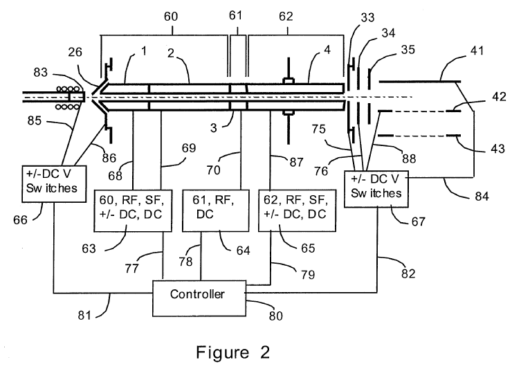
This place covers:
e.g. EP1220291
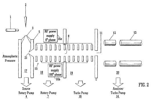
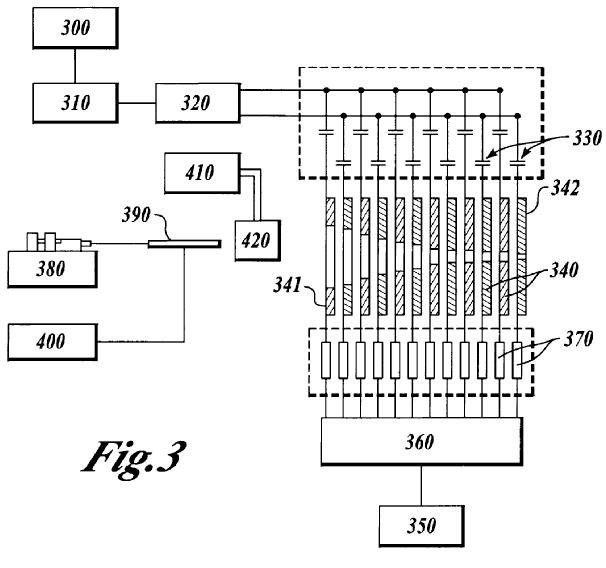
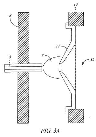
This place covers:
e.g. GB2143673
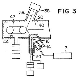
This place covers:
e.g. US6452167
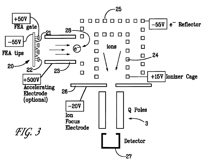
This place covers:
e.g. US5763875
This place covers:
e.g. WO9963576
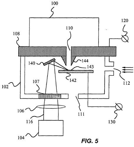
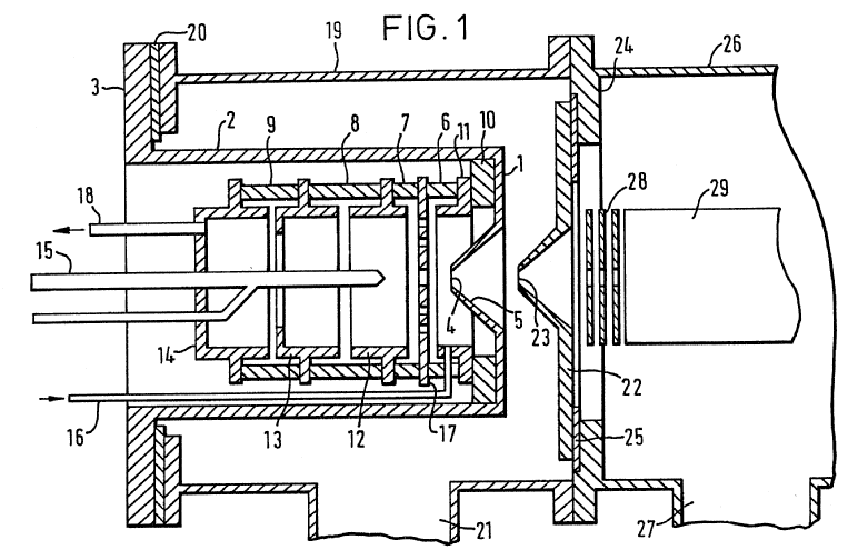
This place covers:
e.g. EP0566022
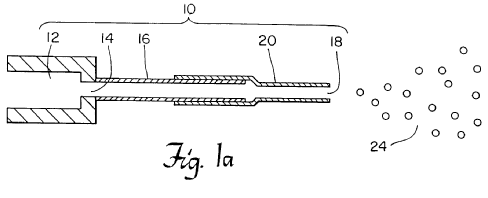
Examples of places where the subject matter of this place is covered when specially adapted, used for a particular purpose, or incorporated in a larger system:
Separation of different isotopes of the same chemical element by mass spectrography | |
Ion-mobility spectrometry combined with mass spectrometry, for investigating the ionisation of gases |
This place covers:
e.g. US4019989
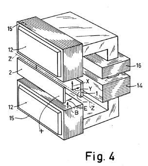
This place covers:
e.g. US3622781
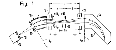
This place covers:
e.g. US5304799
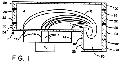
This place covers:
e.g. US2955204
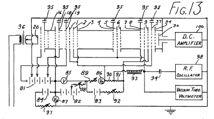
This place covers:
e.g. WO03069651
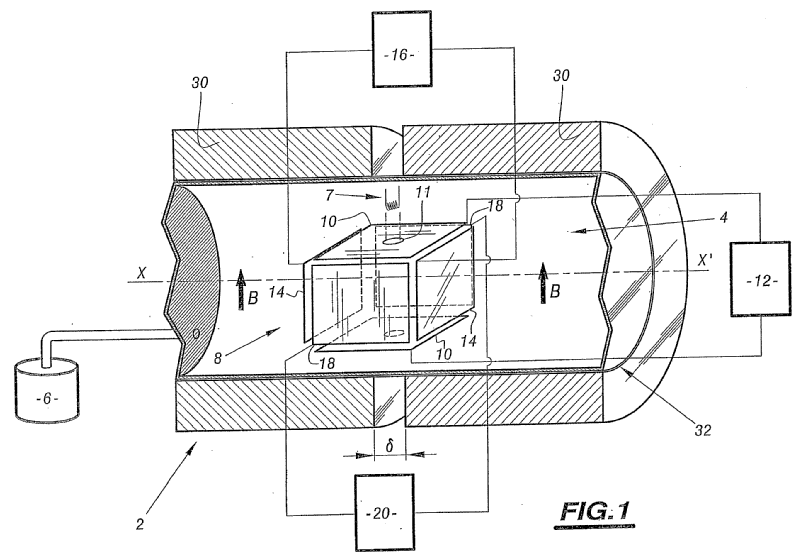
This place covers:
e.g. US5763878
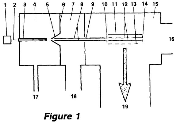
This place covers:
e.g. GB2402545
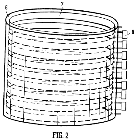
This place covers:
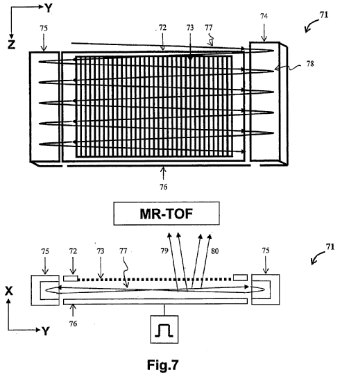
Attention is drawn to the following places, which may be of interest for search:
Electrostatic traps |
This place covers:
e.g. US7227131
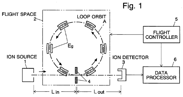
This place covers:
e.g. EP2299471
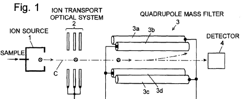
This place covers:
e.g. WO9707530
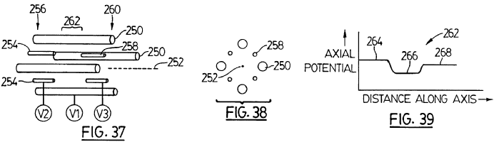
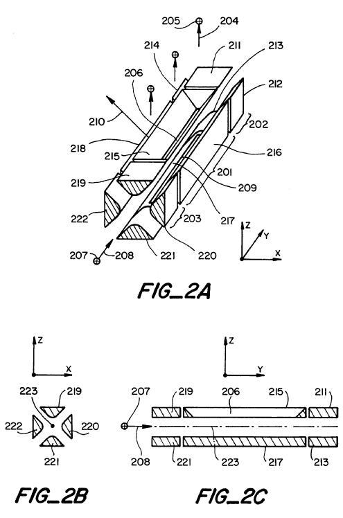
This place covers:
e.g. US5654542
This place covers:
This place does not cover:
Two-dimensional RF ion traps |
Attention is drawn to the following places, which may be of interest for search:
Multi-reflection time of flight spectrometers |
This place covers:
e.g. EP1371081
This place covers:
Gas- or vapour-discharge lamps with main electrodes inside the vessel, and details thereof. In these lamps, the electrodes are not insulated from the discharge, e. g. by dielectric layers.
Examples of the discharge lamps covered here are:
- Low pressure discharge lamps, e. g. fluorescent lamps; compact fluorescent lamps;
- High pressure discharge lamps, e. g. high pressure mercury, sodium, xenon, or metal halide lamps;
- Gas filled flash lamps.
Lamps may further have one (or more) outer envelopes (e.g. a reflector lamp comprising an integral assembly of lamp and reflector; a discharge lamp for a vehicle headlight with an outer envelope); these are classified in H01J 61/00 as long as the lamp and outer envelope are integrally formed or connected with each other and form one single item which can be connected to the power supply connector. The combination of a reflector comprising a lamp socket and a corresponding (replaceable) lamp is considered as a lighting system and is classified in the appropriate classes in F21V or F21S.
This place does not cover:
Electric arc lamps with consumable electrodes | |
Electroluminescent light sources | |
Electric light sources using a combination of different types of light generation | |
Circuit arrangements or apparatus for igniting or operating discharge lamps |
Examples of places where the subject matter of this place is covered when specially adapted, used for a particular purpose, or incorporated in a larger system:
Use of discharge lamps for sterilising milk products | |
Use of discharge lamps for medical purposes, medical equipment using discharge lamps, tanning devices | |
Non-portable lighting devices or systems thereof | |
Details of lighting devices, of general application |
Attention is drawn to the following places, which may be of interest for search:
DC plasma displays | |
Cathode-ray or electron-stream lamps, a phosphor or a gas is brought to luminescence by an electron beam | |
Lamps without any electrode inside the vessel; Lamps with at least one main electrode outside the vessel, electrodeless lamps | |
Chemical, physical, or physico-chemical processes employing the direct application of incoherent waves, e. g. ultraviolet light | |
Use of discharge lamps for disinfecting water, disinfecting apparatus | |
Luminaires or lighting devices containing a lamp | |
Use of discharge lamps for advertising, displays using discharge lamps | |
Adapters and connectors | |
Plasma discharge EUV light sources, in which a gas is locally compressed to create a discharge space and then allowed to expand into a vacuum | |
X-ray radiation generated from plasma, e. g. EUV light sources |
Lamp details are classified in group H01J 61/02 and subgroups thereof, if the details are integral with the lamp or directly attached or applied to the lamp, so that these go with the lamp when the lamp is removed from the power supply connector.
In this place, the following terms or expressions are used with the meaning indicated:
HID lamp | High intensity discharge lamp |
HPS lamp | High pressure sodium lamp |
MH lamp | High pressure metal halide lamp |
CFL | Compact fluorescent lamp |
CCFL | Cold cathode fluorescent lamp |
CRI | Colour rendering index |
Lamp | a lamp comprises the discharge vessel and all peripheral accessories which makes the lamp ready for being plugged in the appropriate power supply connector, i.e. the lamp "ends" with the first suitable connector which can be connected to a standardized or another suitable power supply connector. |
This place covers:
Details of gas or vapour discharge lamps covered by H01J 61/68 - H01J 61/98 and H01J 65/00.
Optical elements have an influence on the light distribution, e.g. focusing or changing the light emission characteristic
Further information:
Details within this group particularly suited for one or more specific lamp types are additionally covered by the appropriate subgroups for the relevant lamp type(s) in H01J 61/58 - H01J 61/98 and H01J 65/00.
This place does not cover:
Attention is drawn to the following places, which may be of interest for search:
Details of electrodes, of magnetic control means, of screens, or of the mounting or spacing thereof, common to two or more basic types of discharge tubes or lamps | |
Details relating to vessels or to leading-in conductors common to two or more basic types of discharge tubes or lamps | |
Details of incandescent lamps |
A subgroup for lamp sockets or bases is missing in H01J 61/00. These are classified in H01J 5/48 - H01J 61/62.
This place covers:
Optical elements integrally associated with the discharge lamp for influencing the spatial distribution of the emitted light:
- Refractive or reflective elements.
- Shields for production of specific dark/bright patterns.
This place does not cover:
Electrodes for igniting the lamp or used as starting aids |
This place does not cover:
Heat-reflecting coatings on the wall of the vessel |
This place covers:
Main electrodes for discharge lamps of the types covered by H01J 61/58 - H01J 61/98 and in H01J 65/00.
Attention is drawn to the following places, which may be of interest for search:
Alloys based on tungsten or molybdenum |
This place does not cover:
Means for influencing the discharge using magnetic means |
This place covers:
Substances for gas fillings necessary for the operation of the discharge lamp, i. e. for
- the generation of the initial discharge,
- generating the voltage gradient,
- light emission,
- for establishing the desired spectral characteristics of the emitted light.
Gases added in small amounts, and which are not necessarily required for the operation of the lamp, are covered by the group reflecting the purpose of the gas filling, if available, otherwise in H01J 61/12.
Examples:
- Gases inside the discharge tube used for gettering or for avoiding blackening of the envelope H01J 61/26.
- Gas filled in the gap between outer envelope and discharge tube in a double-walled lamp H01J 61/34.
- Gas filled in cavities which serve as starting aid H01J 61/54.
In this place, the following terms or expressions are used with the meaning indicated:
Main constituent or principal constituent | should be construed as that filling component which is mainly responsive for the light emission. In many cases, the lamp contains a buffer gas, e.g. argon or xenon, which is necessary for initiating the discharge, but the main part of the light emission is provided for example by mercury or sodium vapour, a metal halide or other chemical substances which emits light in the conditions prevailing in the buffer gas discharge. |
This place covers:
Lamps which exclusively are filled with rare gases
This place does not cover:
Low pressure mercury vapour discharge lamp |
Attention is drawn to the following places, which may be of interest for search:
Composition of metal halide filling of metal halide lamps |
Attention is drawn to the following places, which may be of interest for search:
Means for maintaining the desired pressure within the vessels of two or more basic types of discharge tubes |
Attention is drawn to the following places, which may be of interest for search:
Means for absorbing or adsorbing gas, e.g. by gettering, common to two or more basic types of discharge tubes |
Attention is drawn to the following places, which may be of interest for search:
Means for producing, introducing, or replenishing gas or vapour during operation of two or more the lamp |
Attention is drawn to the following places, which may be of interest for search:
Glass compositions | |
Compositions for glass with special properties | |
Shaped ceramic products characterised by their composition | |
Coatings produced by application to, or surface treatment of, optical elements, e.g. anti-reflection coatings | |
Details of incandescent lamps |
This place does not cover:
Flat vessels or containers of gas discharge lamps |
This place does not cover:
Compact fluorescent lamps |
This place covers:
Fluorescent lamps with folded discharge path and with integral driving circuit, e. g. within the lamp base or socket, such that the lamp can replace incandescent lamps in common lighting fixtures
This place covers:
Examples:
- Discharge tubes with two or more walls.
- Lamps with a discharge tube enclosed in an outer envelope, e. g. high or low pressure discharge lamps with outer envelope.
- Reflector lamps containing a discharge tube within a closed reflector.
- Compact fluorescent lamps with outer envelope.
- Shatterproof enclosures directly mounted on the lamp, e. g. fluorescent lamps with a solid sleeve having shatterproof properties.
This place does not cover:
Lamps with open reflectors |
This place covers:
Coatings on the walls of discharge lamps.
Examples:
- Coatings on the walls of discharge tubes or of the outer envelope of double-walled lamps covered by H01J 61/34.
- Heat or UV-reflective coatings.
- Protective coatings.
- Shatterproof coatings applied to the external surface of the discharge lamp, e. g. by extrusion so as to directly adhere to the discharge tube.
This place does not cover:
Coloured coatings in or on the envelope | |
Devices for influencing the colour or wavelength of the light by transforming the wavelength of the light by luminescence |
Attention is drawn to the following places, which may be of interest for search:
Envelopes, vessels of incandescent lamps provided with coatings on the walls |
This place covers:
Light filters, coatings for influencing the wavelength or the colour of the emitted light, reflective or light diffusing coatings
This place does not cover:
Devices for influencing the colour or wavelength of the light may be applied on the surface or the discharge tube or on the surfaces of outer envelopes of the lamps |
Non-chemical aspects of luminescent materials are covered by H01J 2261/385 , Examples:
Variable thickness profile of layers of luminescent material.
Spatial distribution of luminescent material on lamp surfaces.
This place covers:
Devices for transforming the wavelength of the light by luminescence:
Phosphor coatings characterized by non-chemical parameters, e.g. thickness profile, geometrical characteristics of the phosphor distribution on the vessel surface
This place covers:
Means for cooling specific parts of discharge tube in the form of ribs or other structures integrally formed on or directly attached to the vessel in order to increase the surface of the vessel
This place does not cover:
Heating or cooling arrangements to promote ionisation for starting |
Attention is drawn to the following places, which may be of interest for search:
Arrangement of a lamp and an external cooling fan |
This place covers:
- One or more circuit elements structurally associated with the lamp, the circuit elements must be structurally associated with the lamp. Many compact fluorescent lamps are characterized by an electronic ballast contained in the lamp base.
- Specific arrangements of the components in the lamp base
Attention is drawn to the following places, which may be of interest for search:
Electronic ballasts or driving circuits per se |
This place covers:
Discharge lamps having one or more specially shaped cathodes
Examples:
- for advertising purposes,
- for displaying alphanumeric characters.
This place covers:
Lamps with low-pressure unconstricted discharge.
The cold pressure limit <400 Torr is disregarded.
A fluorescent lamp containing a specific xenon-argon mix as buffer gas, mercury, and a specific phosphor mix with a specific mass density yields a power saving lamp with a higher lumen output per foot arc length should be classified in H01J 61/72. Nevertheless, the document should also be given the group symbols H01J 61/20 and H01J 61/44.
This place covers:
Lamps with high-pressure unconstricted discharge.
The cold pressure limit >400 Torr is disregarded.
This place covers:
- Lamps with different discharge paths
- Lamps with one discharge vessel with a plurality of electrode pairs which form a plurality of discharge paths; these can be separated from each other by walls.
- Arrays of single path discharge lamps, if the array is contained in one common container which provides electrical connection to all single lamps. An example is an array of single fluorescent tubes in a parallel arrangement in a LCD backlight.
This place does not cover:
Incandescent lamps with a filament heated only by non-luminous discharge |
Attention is drawn to the following places, which may be of interest for search:
Incandescent lamps with a filament heated only by non-luminous discharge |
This place covers:
Lamps and details of lamps in which an electron beam excites a luminescent material or a gas to emit light:
- Lamps in which an electron beam strikes a phosphor and excites the phosphor to luminescence
- Lamps in which an electron beam excites a gas to luminescence
Further information:
Details of cathode ray lamps which are also mentioned in a document to be suitable for a display tube are also covered by H01J 29/00 and H01J 31/00.
Attention is drawn to the following places, which may be of interest for search:
Field emissive cathodes | |
Electron guns using field emission | |
Methods for manufacturing details of cathode ray or electron stream lamps | |
Details of display tubes | |
Display tubes |
Attention is drawn to the following places, which may be of interest for search:
Field emission displays |
Attention is drawn to the following places, which may be of interest for search:
Field emission displays |
The more recent lamps which are classified in H01J 63/06 are structurally very similar or identical to field emission displays (H01J 31/123). In order to be classified in H01J 63/06, the document should state or strongly imply the use as a lamp, e.g. a backlight for an LCD display - it is not sufficient that the document refer to a "light emitting element" or use a similar term which also would be applicable to a single pixel or to a whole field emitter display (FED). If both uses (FED and lamp) are mentioned, the document is classified in both subclasses
This place covers:
Lamps without any electrode inside the vessel and electrodeless lamps, and details thereof:
- Microwave excited lamps in which the discharge tube is located in a microwave cavity
- Inductively coupled RF lamps in which the discharge tube is surrounded by an RF coil or antenna
- Lamps with external electrodes only
- Lamps with at least one main electrode outside the vessel
- Lamps in which the main electrodes are inside the vessel, but are separated from the discharge by a dielectric layer
- Lamps with a gas filling excited by internal or external corpuscular radiation
This place does not cover:
Plasma displays | |
Indicating arrangements for variable information in which the desired character or characters are formed by combining individual elements being gas discharge devices | |
Circuit arrangements or apparatus for igniting or operating discharge lamps |
Attention is drawn to the following places, which may be of interest for search:
Details of the lamps covered by H01J 65/00 are covered by the appropriate subgroup for lamp types in H01J 65/00 and, if available, also by the appropriate detail subgroups in H01J 61/00.
Main electrodes | |
Substances for gas fillings | |
Material of the discharge tubes | |
Ignition aids |
Means for coupling electromagnetic energy into the discharge tube are considered as a part of the lamp:
- Microwave or RF cavities, resonators, and waveguides in which the discharge tube is arranged
- RF coils or antennae surrounding or adjacent discharge tube
This place covers:
Lamps in which a screen or coating is excited to luminesce by radioactive material located inside the vessel.
This place does not cover:
Direct conversion of radiation energy from radioactive sources into light |
Attention is drawn to the following places, which may be of interest for search:
Plasma display panels making use of direct current |
Attention is drawn to the following places, which may be of interest for search:
Control arrangements for presentation of assembly of a number of characters using luminous gas-discharge panels |
Attention is drawn to the following places, which may be of interest for search:
Printed circuits; Manufacture of assemblages of electrical components |
Attention is drawn to the following places, which may be of interest for search:
Plasma display panels with alternate current induction of the discharge |
Attention is drawn to the following places, which may be of interest for search:
Electrodes common to discharge tubes | |
Electrodes for display panels, e.g. not making use of alternating current |
This place covers:
Targets which are in fluid state, including targets intended to melt during operation of the X-ray tube.
This place covers:
Targets made of more than one layer of material intended to emit X-rays.
This place does not cover:
Targets with layered structure including a single emissive layer, the other layers serving to improve the mechanical properties, the thermal properties. |
This place covers:
Examples:
Rotating, hollow anodes cooled by water passed along the axis,
Cooling conduits that must be rotated during operation
This place covers:
Example:
Rotating the vessel for positioning purposes
This place does not cover:
Rotation of X-ray vessel where vessel is fixedly joint to anode in order to spread the heat e.g. Straton tube: |
This place covers:
Shielding of X-ray vessels or other components of the tube e.g. against charged particles such as scattered or secondary electrons. Examples:
corona shields;
magnetic fields for shielding;
conductive layers
This place covers:
Structures transparent to x-rays but separating a space of certain properties e. g. ambient pressure from a space having different respective properties e. g. low pressure; including windows acting as target anodes.
This place covers:
Further information:
The codes in this main group are grouped according to the following principle:
details common to gas or plasma discharge of the above mentioned tubes: H01J 2237/00 - H01J 2237/2487
imaging
or analysing: H01J 2237/25 - H01J 2237/2857
particlebeam processing: H01J 2237/30 - H01J 2237/31747
plasma processing: H01J 2237/32 - H01J 2237/339
Codes in the scheme H01J 2237/00 and subgroups are usually marked with the month of their creation ([Nyymm] means "new in month mm of year yy") and are generally not reclassified. These codes are thus are not complete, i.e. not all documents classified in subgroups of H01J 37/00, for which a respective code in subgroups of H01J 2237/00 would be adequate, have such a code.
All limiting references or precedence rules within H01J 2237/00 and subgroups thereof apply only within H01J 2237/00 (and subgroups thereof) and in particular not in view of groups the scheme H01J 37/00 and subgroups thereof, if not a group in H01J 37/00 or below is explicitly referred to.
General Reminder:
For features of general interest which may be found in other types of discharge tubes, an indexing-code corresponding to general schemes H01J 2201/00 - H01J 2217/00 is given, e.g. for cathodes, vessels, cooling means or the like.
Same rules apply for manufacturing procedures (H01J 2209/00), unless really specific to the tube concerned.
Attention is drawn to the following places, which may be of interest for search:
Maintaining constant desired temperature of objects being observed or treated |
This place does not cover:
Gas supply means for processing objects by plasma generation |
Attention is drawn to the following places, which may be of interest for search:
Environmental cells for electron microscopes | |
Microscopes with environmental specimen chamber |
Attention is drawn to the following places, which may be of interest for search:
Movable supports of diaphragms, i.e. for changing between differently sized apertures | |
Movement of the objects being observed or treated |
This place covers:
Shields - both shielding the beam from influence thereon and shielding the environment from influence due to the tube
Attention is drawn to the following places, which may be of interest for search:
Individual lenses |
In this place, the following terms or expressions are used with the meaning indicated:
analysis in H01J 2237/05 and subgroups relates to forming a spectrum; filtering relates to selecting mass or energy of (one) particular value(s)
This place does not cover:
Beam diagnostics anywhere in beam |
Further information:
Diagnostics only for the source
This place does not cover:
Ion sources for mass spectrometers |
This place covers:
gas cluster ion beam sources and other cluster beam ion sources (cluster in this respect means a group of similar atoms or molecules)
acronym for gas cluster ion beam : GCIB
Attention is drawn to the following places, which may be of interest for search:
Magnetic lenses with superconducting coils |
This place covers:
Example:
What is called "scan rotation" in SEMs
Attention is drawn to the following places, which may be of interest for search:
Neutralising arrangements |
Attention is drawn to the following places, which may be of interest for search:
Liner tubes of shields |
This place covers:
Both means and methods
This place covers:
Example:
Also specific arrangements for differential pressure of field emission guns
This place covers:
Both heating and/or cooling
This place covers:
Controlling the environment of the sample in view of e.g. gas pressure, specific types of gases or gas composition, etc.
Attention is drawn to the following places, which may be of interest for search:
Elevated pressure | |
Environmental microscopes |
This place covers:
Vacuum seals associated with the stage, e.g. seals for adjustment screws of the sample stage
This place covers:
Moving the sample such that it stays in focus
This place covers:
Example:
Temperature dilation of positioning element used to move sample
Attention is drawn to the following places, which may be of interest for search:
Vacuum locks |
Attention is drawn to the following places, which may be of interest for search:
Maintaining constant desired temperature of the objects being observed or treated |
This place covers:
Surface alteration of samples to be analysed or inspected, e.g. ion bombardment to modify sample surface in an SEM
This place does not cover:
Processing of objects per se |
Attention is drawn to the following places, which may be of interest for search:
Individual lenses |
Attention is drawn to the following places, which may be of interest for search:
Signal processing, e.g. mixing of two or more signals | |
Image data processing or generation |
Attention is drawn to the following places, which may be of interest for search:
Electron or ion microscopes for holography | |
Holographic processes or apparatus using particles or using waves |
This place does not cover:
Beam diagnostics including respective control |
This place does not cover:
Controlling the beam in electron or ion beam tubes for processing objects |
Attention is drawn to the following places, which may be of interest for search:
Means for deflecting or directing discharge |
This place covers:
Example:
Voltage contrast, charging of sample, leakage current in sample to sample holder, magnetic imaging of sample
Attention is drawn to the following places, which may be of interest for search:
When related to the tube |
This place covers:
Example:
Focus control by additional light-optical microscopes
This place covers:
Microprobes using tunnel effect only in combination with tubes of H01J 37/00, e.g. LEED or RHEED in combination with STM
This place does not cover:
STM, AFM, etc. per se |
Attention is drawn to the following places, which may be of interest for search:
Environmental cells |
This place does not cover:
Treatment of data |
Attention is drawn to the following places, which may be of interest for search:
Holographic processes or apparatus using particles |
This place covers:
Example:
Methods for image compare
Attention is drawn to the following places, which may be of interest for search:
System calibration of electron or ion beam tubes for processing objects |
Attention is drawn to the following places, which may be of interest for search:
Particle-beam lithography, e.g. electron beam lithography |
Attention is drawn to the following places, which may be of interest for search:
Calibration of electron or ion microscopes |
Attention is drawn to the following places, which may be of interest for search:
Means for deflecting or directing discharge | |
Scanning the beam |
Attention is drawn to the following places, which may be of interest for search:
Detecting endpoint of process for plasma apparatus | |
Detecting exhaustion of target material in gas-filled discharge tubes operating with cathodic sputtering |
This place covers:
Control of contamination stemming from the ion source or beam line
Attention is drawn to the following places, which may be of interest for search:
Ion plating |
Attention is drawn to the following places, which may be of interest for search:
Pattern inspection | |
Direct-write microstructures | |
Etching microareas |