CPC Definition - Subclass H01L
This place covers:
in general
- discrete and integrated semiconductor devices and
- other electric solid state devices (as far as not provided for in another subclass) and
- details thereof.
This includes the following kind of devices:
- integrated circuit devices, e.g. CMOS integrated devices, DRAM, EPROM or CCD;
- semiconductor devices (e.g. field-effect, bipolar) adapted for rectifying, amplifying, oscillating or switching, e.g. diodes, transistors or thyristors;
- semiconductor devices sensitive to radiation, e.g. photo diodes, photo transistors or solar cells;
- incoherent light emitting diodes, e.g. LED;
- solid state devices using organic materials as the active part or using a combination of organic materials with other materials as the active part, e.g. organic LED or polymer LED;
- electric solid state devices using thermoelectric, superconductive, piezoelectric, electrostrictive, magnetostrictive, galvano-magnetic or bulk negative resistance effects, e.g. thermo couples, Peltier elements, Josephson elements, piezo elements;
- photo-resistors, magnetic field dependent resistors or field effect resistors;
- capacitors having potential barriers or resistors having potential barriers;
- thin-film or thick-film circuits;
- processes and apparatus adapted for the manufacture or treatment of such devices, except where such processes relate to single step processes for which provision exists elsewhere.
Microstructural devices or systems are classified in subclass B81B, and the processes and apparatus specially adapted for the manufacture or treatment thereof are classified in subclass B81C. So, by way of example, microelectro-mechanical devices (MEMS), containing microelectronic and mechanical components, are classified in group B81B 7/02, and their manufacture, treatment or assembling in the relevant groups of B81C. Microstructural devices or systems working purely electrically or electronically, or related processes or apparatus for the manufacture or treatment thereof are, however, not covered by B81B or B81C and are classified in section H, for example in the groups of the current subclass H01L.
Microstructural devices or systems being of other than purely electrical or electronically type, and apparatus or processes for the manufacture or treatment thereof, which are normally classified in the subclasses B81B and B81C, may be also classified in those groups of H01L providing for their structural or functional features, whenever such features are of interest per se.
This place does not cover:
Use of semiconductor devices for measuring | |
Non-adjustable resistors from semiconductor material | |
Magnets, inductors, transformers | |
Capacitors in general | |
Electrolytic devices | |
Batteries, accumulators | |
Waveguides, resonators or lines of the waveguide type | |
Line connectors, current collectors | |
Lasers, stimulated emission devices, e.g. semiconductor laser | |
Electromechanical resonators; impedance networks | |
Loudspeakers, microphones, gramophone pick-ups or like acoustic electromechanical transducers | |
Electric light sources in general | |
Printed circuits, hybrid circuits, casings or constructional details of electric apparatus, manufacture of assemblages of electrical components |
Attention is drawn to the following places, which may be of interest for search:
Containers merely intended for transport or storage of wafers except during manufacture or finishing devices thereon | |
Conveying systems for semiconductor wafers except during manufacture or treatment of semiconductor or electric solid state devices or components thereon | |
Micromechanical Devices (MEMS) | |
Processes and apparatus specially adapted for the manufacture or treatment of microstructural devices or systems | |
Coating Material | |
Non-mechanical removal of metallic material from surface | |
Measurement of Mechanical Vibrations or Ultrasonic, Sonic or Infrasonic Waves | |
Measurement of Intensity, velocity, Spectral, Content, Polarization, Phase or Pulse Characteristic of Infrared, Visible or Ultraviolet Light | |
Measuring Electrical or Magnetic Variables | |
Details of scanning-probe apparatus, in general | |
Radio Direction-Finding; Radio Navigation; Determining Distance or Velocity by Use of Radio Waves; Locating or Presence-Detecting by Use of the Reflection or Reradiation of Radio Waves; Analogous Arrangements Using Other Waves | |
Measuring Nuclear or X-Radiation | |
Electro photography | |
Systems for Regulating Electrical or Magnetic Variables | |
Digital Computers | |
Static Stores | |
Conductive and Insulating Materials | |
Electric discharge tubes or discharge lamps | |
Amplifiers | |
Pictorial Communication, e.g. Television |
In this subclass, Indexing Codes are mainly attributed with a view to allow retrieval of documents comprising a combination of technical characteristics, some of them being unimportant per se, and, hence, identified as additional information rather than invention information.
In this subclass, both the process and apparatus for the manufacture or treatment of a device and the device itself are classified, whenever both of these are described sufficiently to be of interest.
In this place, the following terms or expressions are used with the meaning indicated:
assembly of a device | the "assembly" of a device is the building up of the device from its component constructional units and includes the provision of fillings in containers. |
complete device | a "complete device" is a device in its fully assembled state which may or may not require further treatment, e.g. electro-forming, before it is ready for use but which does not require the addition of further structural units. |
component | a "component" is one electric circuit element of a plurality of elements formed in or on a common substrate. |
container | a "container" is an enclosure forming part of the complete device and is essentially a solid construction in which the body of the device is placed, or which is formed around the body without forming an intimate layer thereon. |
device | the term "device" refers to an electric circuit element; where an electric circuit element is one of a plurality of elements formed in or on a common substrate it is referred to as a "component". |
electrodes | "electrodes" are regions in or on the body of the device (other than the solid-state body itself), which exert an influence on the solid-state body electrically, whether or not an external electrical connection is made thereto. An electrode may include several portions and the term includes metallic regions which exert influence on the solid-state body through an insulating region (e.g. capacitive coupling) and inductive coupling arrangements to the body. The dielectric region in a capacitive arrangement is regarded as part of the electrode. In arrangements including several portions only those portions which exert an influence on the solid-state body by virtue of their shape, size or disposition or the material of which they are formed are considered to be part of the electrode. The other portions are considered to be "arrangements for conducting electric current to or from the solid-state body" or "interconnections between solid state components formed in or on a common substrate", i.e. leads. |
encapsulation | an "encapsulation" is an enclosure which consists of one or more layers formed on the body and in intimate contact therewith. |
integrated circuit | an "integrated circuit" is a device where all components, e.g. diodes, resistors, are built up on a common substrate and form the device including interconnections between the components. |
integration process | processes for the manufacture of at least two different components where the process is especially adapted to their integration, e.g. to take advantage of the integration or to reduce their manufacturing cost. Example: in a CMOS process, the same ion implant dopes the p-MOS gate and the n-MOS source and drain. Consequently, a process for the manufacture of a component per se is not considered as an integration process, even though that component will be part of an integrated circuit. |
interconnection | refers to the arrangement of conductive and insulating regions aimed at electrically connecting the respective electrodes of at least two device units, e.g. two transistors. |
parts | the term "parts" includes all structural units which are included in a complete "device". |
solid state body | the expression "solid state body" refers to the body of material within which, or at the surface of which, the physical effects characteristic of the device occur. In thermoelectric devices it includes all materials in the current path. |
wafer | a "wafer" means a slice of semiconductor or crystalline substrate material, which can be modified by impurity diffusion (doping), ion implantation or epitaxy, and whose active surface can be processed into arrays of discrete devices or integrated circuits. |
In patent documents, the following words/expressions are often used with the meaning indicated:
package | container, encapsulation. |
This place covers:
Processes and apparatus that are specially adapted for the manufacturing of semiconductor or solid state devices belonging to the type:
- Integrated circuit devices, e.g. CMOS integrated devices, DRAM, EPROM, CCD;
- Semiconductor devices (e.g. field-effect, bipolar) adapted for rectifying, amplifying, oscillating or switching, e.g. diodes, transistors, thyristors;
This main group includes;
- Manufacture or treatment of the above semiconductor devices or of parts thereof
- Manufacture or treatment of solid state devices other than semiconductor devices, or of parts thereof
- Apparatus specially adapted for handling semiconductor or electric solid state devices during manufacture or treatment thereof; Apparatus specially adapted for handling wafers during manufacture or treatment of semiconductor or electric solid state devices or components
- Manufacture or treatment of devices consisting of a plurality of solid state components formed in or on a common substrate or of parts thereof; manufacture of integrated circuit devices or of parts thereof
Attention is drawn to the following places, which may be of interest for search:
Processes for applying liquids or other fluent materials | |
Liquid cleaning (in general) | |
Machines, Devices, or Processes for Grinding or Polishing | |
Containers, packaging elements or packages specially adapted for particular articles or materials | |
Shaped ceramic Products | |
Polishing compositions | |
Cleaning Compositions | |
Coating by vacuum evaporation, by sputtering or by ion implantation of the coating forming material | |
Chemical coating by decomposition of gaseous compounds, without leaving reaction products of surface material in the coating (CVD) | |
Chemical coating by decomposition of either liquid compounds or solutions of the coating forming compounds,without leaving reaction products of surface material in the coating | |
Etching metallic material by chemical means | |
Processes for the Electrolytic or Electrophoretic Production of Coatings | |
Single Crystal Growth; Epitaxy | |
Testing individual semiconductor devices | |
Preparation of originals for the photomechanical production of textured or patterned surfaces | |
Photolithographic, production of textured or patterned surfaces | |
Registration or positioning of originals, masks, frames, photographic sheets or textured or patterned surfaces | |
Discharge tubes with provision for introducing objects or material to be exposed to the discharge (plasma etching; ion implantation) | |
Apparatus or processes specially adapted for manufacturing or adjusting assemblages of electric components | |
Processes or apparatus specially adapted for the manufacture or treatment of devices or parts thereof |
Single mono-steps for which a provision exists elsewhere in CPC need not to be classified in H01L 21/00, except if they are specific to the fabrication of semiconductor devices as defined under H01L 21/00. E.g., apparatuses which are not specific to the fabrication of these devices, e.g. apparatuses for depositing layers, are classified in C23C or C30B.
Direct pre-treatment or direct post-treatment of a specific step is classified under the specific step if no other place exists in H01L 21/00. Example: annealing after layer coating is classified together with the coating. Exception: cleaning, see H01L 21/02041
In H01L 21/00, poly-silicon is generally considered as a conductive material for classification purposes, except for its deposition (H01L 21/02365) where it is considered as semiconducting.
Polishing or chemical-mechanical polishing are not distinguished for classification.
Machines and apparatuses for which a provision exists somewhere else in CPC are not classified In H01L 21/00. For example apparatus for deposition of materials are classified in C23C or C30B.
Machines and apparatuses for which no particular provision exists in CPC are classified in H01L 21/67 and subgroups. See also the notes under H01L 21/67.
Processes mainly consisting of features of the use of the elements of the apparatus and which are necessary to operate said apparatus (like for example rotating the turntable of a polisher, evacuating the chamber of a plasma appraratus etc...) need not to be classified in H01L 21/00.
Subject matter relating to processes and apparatus which are clearly suitable for manufacture or treatment of devices whose bodies comprise elements of the fourth group of the Periodic Table (silicon, germanium), and where the material used is not explicitly specified, is classified in the subgroups relating to semiconductors of the fourth group of the Periodic Table (silicon, germanium).
For multistep processes, a junction between two regions of the same material but in a different crystalline state, e.g. amorphous silicon or polysilicon emitters on single crystalline silicon, is not considered as a heterojunction.
In this place, the following terms or expressions are used with the meaning indicated:
Dry Process | refers to processes wherein only gases or vapours are provided on the surface of a substrate, e.g. a wafer, irrespective of the physical state of the reaction products, gaseous, liquid or solid. |
Wet Process | refers to processes wherein only liquids are provided at the surface of a wafer, including the condensation on the surface of a wafer of gaseous components. |
Pre-, post-treatment | direct, for example in situ, treatment, preceding or following a main technological step, aimed at improving said main technological step or its result. Not considered as a technological step per se. Examples: - annealing or crystallisation after deposition of insulating layers, - cleaning before or after a technological step, - modifying an insulating layer just after its formation, e.g. implantation after deposition |
After treatment | Subsequent main technological step. Examples: - patterning or polishing of a layer after deposition- modifying an insulating layer after a step which is not the formation of the insulating layer |
In patent documents, the following abbreviations are often used:
CVD | Chemical vapour deposition |
PECVD | Plasma enhanced CVD |
LPCVD | Low pressure CVD |
PVD | Physical Vapour Deposition |
ALD | Atomic layer deposition |
ALE | Atomic layer epitaxy |
CMP | Chemical mechanical polishing |
ECMP | Electrochemical CMP |
SOI | Silicon on Insulator |
BESOI | Bonded and Etched-Back Silicon-On-Insulator |
SOS | Silicon on Sapphire |
HSG | Hemispherical grain |
RIE | Reactive ion etching |
BSG | boron silicate glass |
PSG | phosphorous silicate glass |
BPSG | boron phosphorous silicate glass |
USG | Undoped silicate glass |
FSG | Fluorine silicate glass |
PZT | Lead zirconate titanate |
BST | Barium strontium titanate |
HSQ | Hydrogen silsesquioxane |
MBE | Molecular beam epitaxy |
ELO | Epitaxial lateral overgrowth |
MIS | Metal-insulator-semiconductor |
MOS | Metal-oxide-semiconductor |
CMOS | Complementary MOS |
DMOS | Double diffused MOS |
VDMOS | Vertical DMOS |
LDMOS | Lateral DMOS |
IMPATT | Impact Ionization Avalanche Transit Time |
TRAPATT | Trapped Plasma Avalanche Triggered Transistor |
SITh | Static induction thyristor |
FCTh | Field controlled thyristor |
IGBT | Insulated Gate Bipolar Transistor |
HET | Hot electron transistor |
SET | Single electron transistor |
SIT | Static Induction Transistor |
MBT | Metal base transistor |
RHET | Resonant tunnelling hot electron transistor |
RTT | Resonant tunnelling transistor |
BBT | Bulk barrier transistor |
PBT | Permeable Base Transistor |
HFET | Heterostructure FET |
HIGFET | Heterostructure Insulated Gate FET |
SISFET | Semiconductor-insulator-semiconductor FET |
HJFET | Hetero Junction FET |
MISFET | Metal-insulator-semiconductor FET |
JFET | Junction FET |
FinFET | FET with Fin-type channel |
MuGFET | Multi Gate FET |
HEMT | High Electron Mobility Transistor |
PDBT | Planar doped barrier transistor |
CHINT | Charge injection transistor |
LDD | lightly doped drain |
DDD | Double diffused drain |
EPIC | Epitaxial Passivated Integrated Circuit |
LOCOS | Local Oxidation of Silicon |
SWAMI | Side Wall Masked Isolation |
SILO | Sealed Isolation LOCOS |
SIMOX | Separation by Implantation of Oxygen |
FIPOS | Full Isolation by porous oxidized silicon |
ELTRAN | Epitaxial Layer Transfer |
SEG | Selective Epitaxial Growth |
DRAM | Dynamic RAM |
CCD | Charge Coupled Device |
This place covers:
Multi-step processes for the manufacture of semiconductor wafers for the fabrication of semiconductor devices as defined under H01L 21/00, prior to the fabrication of any device or part of device, i.e. between the sawing of ingots (covered by B28D) and the cleaning of the wafers (H01L 21/02041), e.g. grinding followed by lapping and polishing.
Covers the preparation of bulk semiconductor wafers (e.g. bulk silicon wafers).
See also H10D 84/00, which has been used for classifying the fabrication of substrates containing parts of Group-IV and Group AIII-BV semiconductors.
See also C30B 33/00.
Attention is drawn to the following places, which may be of interest for search:
Thermal smoothening | |
Fabrication of inhomogeneous wafer, e.g. SOI | |
Marking of wafers | |
Forming flats |
This place covers:
Bulk, homogeneous wafers:
- Group IV, Si, Ge,
- Group III-V, GaAs, InP,
This place covers:
Multistep process for preparing wafers where the accent is put on a specific step.
This place covers:
Multistep process for preparing wafers where the accent is put on the grinding or lapping, e.g. multiple grinding steps.
This place covers:
Multistep process for preparing wafers where the accent is put on the backside treatment.
Includes backside treatment for recognition purposes
This place covers:
Multistep process for preparing wafers where the accent is put on the chemical etching step or steps.
Attention is drawn to the following places, which may be of interest for search:
Chemical or electrical treatment, e.g. electrolytic etching |
This place covers:
Multistep process for preparing wafers where the accent is put on the edge treatment, e.g. chamfering.
This place does not cover:
Does not cover the processing of edges of Smart Cut donor substrates, classified in reclaiming/reprocessing |
This place covers:
Multistep process for preparing wafers where the accent is put on the mirror polishing.
In case a mechanical mirror polishing is completed by a chemical flattening step, e.g. a gaseous flattening step, the latter is classified independently.
This place covers:
Multistep processes for preparing wafers having a specific orientation planes as useful plane, or a specific orientation plane in a plane parallel to the surface.
Attention is drawn to the following places, which may be of interest for search:
Single-crystal growth by pulling from a melt characterised by the seed, e.g. its crystallographic orientation |
This place covers:
Making a surface of the wafer porous. Includes formation of internal porous regions.
This place does not cover:
Localized formation (using e.g. masks) of porous regions |
This place covers:
Multistep processes for reclaiming or re-processing, a wafer containing more than a cleaning process. Also contains the re-processing of Smart-Cut donor substrates.
Attention is drawn to the following places, which may be of interest for search:
Specific cleaning for reclaiming or reprocessing |
This place covers:
Processes adapted to change the shape of a wafer, either in the surface plane (e.g. square, rectangular wafers), or in cross section (bone cross section).
This place does not cover:
The provision of flats, classified with the fabrication of the ingot |
This place covers:
Cleaning of wafers before or during manufacturing;
Cleaning is the removal of entities which were always unwanted, like particles, impurities, stringers, fences etc. Also includes the removal of edge beads or unwanted coatings on edges or backside of the wafers etc., except photoresist edge beads and photoresist on backside.
Removal of entities which have had a use or a function (sidewalls, resists etc.) is not considered to be a cleaning.
Includes the removal of natural oxide, see also the section "Special rules for classification within this group" below.
Starts with the deep cleaning carried out before first fabrication step (Piranha-RCA) up to cleaning after singulation.
Rinsing and drying are seen as a post-treatment of a wet cleaning, classified together with wet cleaning in H01L 21/02052.
This place does not cover:
Does not cover the transformation of an impurity or contaminant in something else remaining on the device, e.g. passivation, classified with passivation in general | |
Processes for the removal of only photoresists, classified in | |
Removal of excess metal after silicidation, classified in | |
Does not cover processes for the removal of photoresists edge beads after coating |
Attention is drawn to the following places, which may be of interest for search:
Cleaning apparatus | |
Cleaning by methods involving the use of tools, brushes, or analogous members, the use or presence of liquid or steam, the use of air flow or gas flow; Cleaning by electrostatic means | |
Detergent compositions, e.g. cleaning solutions or liquids |
Removal of only natural oxide is also classified in H01L 21/311 if the process is of special relevance for thick oxides.
Removal of impurities, e.g. side walls after RIE, together with the photoresist is classified in H01L 21/02041, and additionally in H01L 21/311, if the resist removal method is peculiar.
In patent documents, the following abbreviations are often used:
RCA | standard clean composed of SC-1 and SC-2 at least, with piranha and HF or DHF |
SC-1 | standard clean 1: NH4OH-H2O2 |
SC-2 | standard clean 2: HCl, H2O2 |
DHF | diluted HF |
Piranha | H2SO4-peroxide |
This place covers:
Cleaning of the wafer before any manufacturing step for the device is carried out.
Attention is drawn to the following places, which may be of interest for search:
Does not cover the transformation of an impurity or contaminant in something else remaining on the device, e.g. passivation | |
Processes for the removal of only photoresist | |
Removal of excess metal after silicidation | |
Does not cover processes for the removal of photoresist edge beads after coating |
This place covers:
All cleaning steps are dry, or when the invention is focussed on a dry cleaning aspect, the cleaning also containing more classical wet steps, like RCA.
This place does not cover:
Cleaning of diamond |
This place covers:
Wet cleaning.
This place does not cover:
Cleaning of diamond |
Rinsing and drying are seen as a post-treatment of a wet cleaning, classified together with wet cleaning in H01L 21/02052.
This place covers:
The sequence of combining wet and dry steps.
This place does not cover:
Cleaning of diamond |
Rinsing and drying are seen as a post-treatment of a wet cleaning, classified together wet cleaning in H01L 21/02052.
This place covers:
Cleaning when at least a fabrication step for a device (for example, first oxidation) has been carried out.
This place covers:
- Cleaning after etching gate sidewalls and etching of gate oxide.
- Cleaning after formation of a resist pattern
This place covers:
Reclaiming of semiconductor wafers as well as donor semiconductor wafers, e.g. donors in Smart-Cut®
This place does not cover:
Etching for reclaiming |
This place covers:
Special products to be cleaned, including particular materials as well as substrates comprising particular features, like vertical features, isolated sidewalls, etc.
This place covers:
Removal of edge beads.
This place covers:
Removal of impurities or unwanted materials on backside, including parasitic coatings.
This place covers:
The group covers inventions wherein the mechanical aspect is of particular importance. Does not exclude some enhancement by chemical means.
This place covers:
Covers processes wherein the laser action has a primary function, with or without chemical, mechanical or electrical assistance.
Attention is drawn to the following places, which may be of interest for search:
Cleaning using a laser per se |
This place covers:
Covers processes wherein the supercritical fluid has a primary function, with or without chemical, mechanical or electrical assistance.
This place covers:
Processes for the formation of inorganic and organic layers on a substrate, except photoresist layers (see H01L 21/027), for the fabrication of semiconductor devices as defined under H01L 21/00.
In situ pre- and post-treatments of these processes.
Processes for the formation of a multiplicity of these layers.
Processes for coating materials in general: C23C
Processes for the electrolytic coating of materials in general: C25D
Processes for the single-crystal growth of materials in general: C30B
This place does not cover:
Processes for forming photoresist layers, covered in | |
Processes for forming conductive layers, covered by |
Attention is drawn to the following places, which may be of interest for search:
- Multistep processes for fabricating laminates of insulating and conductive layers, for example insulated gates or capacitors, are classified in the corresponding application, H01L 21/28 for the insulated gates, H10D 1/041 for the capacitors etc. and do not need to be systematically classified in H01L 21/02107. However a group symbol in H01L 21/02107 may be given in case the process for forming the insulating layer is considered of general interest.
In this place, the following terms or expressions are used with the meaning indicated:
ALD | atomic layer deposition |
ALE | atomic layer epitaxy |
MBE | molecular beam epitaxy |
PECVD | plasma enhanced chemical vapour deposition |
PVD | physical vapour deposition |
CVD | chemical vapour deposition |
This place covers:
Processes for the formation of inorganic and organic insulating layers on a substrate, except photoresist layers (see H01L 21/027), for the fabrication of semiconductor devices as defined under H01L 21/00.
In situ pre- and post-treatments of these processes.
Processes for the formation of a multiplicity of these layers.
Includes fabrication of insulating
- porous layers,
- organic layers, like polyimide, cyclobutenes etc.
- Spin On Glass layers,
- silicate layers,
- inorganic layers, like SiO2, Si3N4, Al2O3, high-k layers, perovskites etc.
Processes for coating materials in general, including insulating materials: C23C
Processes for the electrolytic coating of materials in general: C25D
Organic or polymer layer composition: see C08G
This place does not cover:
Processes for forming photoresist layers |
Attention is drawn to the following places, which may be of interest for search:
Photoresist per se |
The process must be adapted or specific to the fabrication of semiconductor devices as defined under H01L 21/00. The mere mentioning of an intended use in semiconductor fabrication does not require that the document being given a group symbol in H01L 21/02107.
If the deposition is specifically adapted to a specific application, with details as to this specific application, e.g. the fabrication of a MIS or MOS electrode or interconnections, the document should additionally be classified in this specific application, for example in H01L 21/28 for the MIS or MOS aspect.
Attention is drawn to the following places, which may be of interest for search:
Layers comprising sub-layers, i.e. multi-layers, are additionally classified in | |
Porous layers are additionally classified in |
This place does not cover:
Carbon Nitride. |
Attention is drawn to the following places, which may be of interest for search:
Halogen doped silicon oxides, e.g. fluorine, containing BPSG, PSG, BSG |
Halogen containing materials, e.g. fluorine, containing BPSG, PSG, BSG, are additionally classified in H01L 21/02131
This place covers:
The formation of silicon oxide layers is classified in this group regardless of the precursor or of the process of formation.
Attention is drawn to the following places, which may be of interest for search:
In case of explicit statements on doping, on rest-groups, or on material components, see | |
Deposition of silicon oxide from organic precursors without further statements on film composition is classified here and in |
This place does not cover:
The formation of material containing Si, O and C, with or without additional elements | |
The formation of material containing Si, O and N, with or without additional elements |
This place does not cover:
The formation of material containing Si, N and C, with or without additional elements | |
The formation of material containing Si, O and N, with or without additional elements |
This place does not cover:
Materials containing silicon | |
Metal silicates |
This place does not cover:
Materials having a perovskite structure, e.g. BaTiO3 |
Perovskites are not classified in H01L 21/02175 and subgroups thereof.
Attention is drawn to the following places, which may be of interest for search:
Adhesion or buffer layers |
This place does not cover:
Mixtures of silane and oxygen |
In this place, the following terms or expressions are used with the meaning indicated:
Alkoxysilane | siloxane |
This place does not cover:
Mixtures of silane and oxygen |
Subject matter classified in the range H01L 21/0223 - H01L 21/02249 is additionally classified in H01L 21/02252, H01L 21/02255, and H01L 21/02258 depending on the type of reaction.
This place does not cover:
After treatment of an insulating film by plasma |
Attention is drawn to the following places, which may be of interest for search:
Formation of an insulating film by introduction of substances into an already existing insulating film is covered by |
This place does not cover:
Formation of insulating layers by plasma treatment, e.g. plasma oxidation of the substrate | |
After treatment of an insulating film by plasma |
This place covers:
Deposition methods in which the gas or vapour is produced by physical means, e.g. ablation from targets or heating of source materials.
This place covers:
Deposition methods in which the gas or vapour is produced by physical means, i.e. by ablation from targets.
This place covers:
- Deposition methods in which the gas or vapour is produced by heating of source materials.
- Molecular beam epitaxy
Attention is drawn to the following places, which may be of interest for search:
Formation of epitaxial insulating films by a deposition method also under |
This place does not cover:
Deposition by physical ablation of a target, like sputtering, reactive sputtering, physical vapour deposition, pulsed laser deposition |
Attention is drawn to the following places, which may be of interest for search:
Deposition by decomposition or reaction of gaseous or vapour phase compounds in the presence of a plasma (PECVD) |
Subject matter relating to cyclic plasma CVD is additionally classified in H01L 21/02274
Attention is drawn to the following places, which may be of interest for search:
Printing in general |
This place does not cover:
Formation of non-epitaxial layers by MBE | |
Atomic layer epitaxy [ALE] |
Attention is drawn to the following places, which may be of interest for search:
Epitaxial growth in general |
This place covers:
Treatments, carried out just before or just after the formation of an insulating layer, which do not participate in the formation of the layer itself, but which are directly linked to the layer formation.
This place does not cover:
Processes participating to the formation of a layer, for example oxidation or nitridation of silicon to form an oxide or nitride layer | |
After treatments like - etching - cleaning - planarising |
Pre- or post treatments of general nature (pre-, post-cleaning, pre-, post conditioning etc.) without details or routine annealing steps, i.e. thermal treatment without further features as to a special atmosphere, presence of a plasma, thermally induced chemical reactions, change of phase or crystal structure, need not to be given this group symbol.
This place covers:
- Treatments to improve adhesion or change the surface termination
This place does not cover:
Treatments by etching |
This place does not cover:
Ex situ cleaning, covered by |
This place covers:
The definition should read "post-treatment" instead of after-treatment.
Only covers processes that are part of the layer formation.
This place does not cover:
After- treatments performed after completion of the insulating layer |
Functionalization just after formation should be classified here.
In case the process would also be of interest as an after treatment (H01L 21/3105), both group symbols should be given.
This place covers:
Processes for introducing substances into the formed insulating layer e.g. introduction of phosphorus into silicon oxide, or introduction of nitrogen into silicon nitride to change stoichiometry.
Attention is drawn to the following places, which may be of interest for search:
For the method of introduction of the dopant |
Introduction of substances into the formed insulating layer is classified both here and in H01L 21/3115
This place covers:
Oxidation of silicon nitride to form silicon oxynitride.
This place covers:
Nitridation of silicon oxide to form silicon oxynitride.
Attention is drawn to the following places, which may be of interest for search:
Subject matter relating to cleaning processes for semiconductor device fabrication | |
Cleaning in general | |
Cleaning compositions in general | C30D |
This place covers:
Processes for the formation of inorganic semiconductors on a substrate.
Processes for forming doped inorganic semiconductors.
In situ pre-and post-treatments of inorganic semiconductor materials.
Processes for the formation of multiple layers of inorganic semiconductors, comprising heterostructures.
The formed semiconductor layer may be crystalline (mono-, poly-, microcrystalline) or amorphous.
This place does not cover:
Nanosized carbon materials, e.g. fullerenes, carbon nanotubes | |
Processes for forming layers only characterized by the purely chemical aspects of the used precursors |
Attention is drawn to the following places, which may be of interest for search:
Formation of inorganic semiconductors for light | |
Processes specially adapted for the manufacture or treatment of organic semiconductor or solid state devices or of parts thereof | |
Fullerenes used in semiconductor or solid state devices |
This place does not cover:
Carbon nanotubes used in semiconductor or solid state devices |
This place does not cover:
Ex situ cleaning |
This place does not cover:
After-treatments for improving the planarity of the layers, e.g. thermal smoothening of layers |
This group is not used for classification; subject matter relating to the formation of conductive material on a semiconductor substrate is classified in H01L 21/283 - H01L 21/288, H01L 21/3205 and H01L 21/768.
This place covers:
Formation of masks to be used for etching or patterning, formed out of a layer formed or deposited on the wafer. Includes inorganic masks (metallic or insulating materials) as well as organic masks.
Composition of photosensitive polymers, see G03F 7/00.
Photographic masks of the stencil tape or originals per se: G03F 1/00
Registration or positioning of photographic masks or originals: G03F 9/00
Photographic cameras G03B
Control of position G05D 3/00
This place does not cover:
masks for selective growth | |
masks for implantation | |
masks for forming insulating layers | |
Formation and use of stencil masks | |
Masks per se, e.g. free standing mask, stencil mask | |
Formation of photoresist masks per se | |
Formation of masks for non patterning purposes: |
Attention is drawn to the following places, which may be of interest for search:
In main group H01L 21/00 and subgroup thereof, a mask is defined as a layer, which is coated directly onto the surface of the wafer.
A free standing mask (stencil mask) laid on the wafer is not considered as a mask in the sense of H01L 21/00.
Masks are classified in H01L 21/00 only under the condition that its treatment or structure has been specially adapted to the fabrication of a device covered by H01L 21/00. Examples are:
- masks used for more than one technological step during device fabrication,
- masks whose structure, formation or treatment are adapted to the nature of the layers or materials used in the fabrication of semiconductor device, or to the device itself
This place covers:
Covers polymeric masks, including photo-sensitive masks (photoresist) as well as non photo-sensitive masks, e.g., wax, polyimide etc.
This place covers:
Treatment of photoresist layers peculiar to fabrication of electronic devices.
H01L 21/0273 covers the treatment of photoresist which is not peculiar to the type of resist (UV, e-beam, ion beam resist), for example:
- method of reflowing the resist,
- method of hardening the resist
Attention is drawn to the following places, which may be of interest for search:
Photoresists and processing of photoresists in general |
- If the treatment is peculiar to the resist type (light, e-beam or ion-beam resist), then it is classified in the corresponding subgroup. If not, remains in H01L 21/0273.
- Chemical amplification is considered to be peculiar to the resist type.
- fabricating masks by irradiating a resist with different types of radiation, e.g. photons and electrons, the document is classified in H01L 21/0273.
This place covers:
Anti-reflective coatings specially adapted for devices as defined under H01L 21/00.
Covers organic as well as inorganic anti-reflective coatings
Attention is drawn to the following places, which may be of interest for search:
Antireflective coatings for lithography in general |
This place covers:
Multilayer structures and special structures adapted to evacuate charges, e.g. multilayer resists with a conductive layer.
Multilayer resists for electrolithography should additionally be classified in G03F 7/00.
This place covers:
Includes multilayer structures.
Multilayer resists for Röntgenlithography should additionally be classified in G03F 7/00
This place covers:
Processes for forming masks comprising inorganic layers.
This group H01L 21/033 acts as a head group for inorganic masks for patterning layers. Multiple classification with H01L 21/31144 (masks for etching insulating layers), H01L 21/32139 (masks for etching conductive layers and polysilicon layers) and H01L 21/308 (masks for etching semiconductors) is possible.
This place covers:
Processes for forming masks to be used for lifting off another layer (for example having a multilayer structure or special profile) irrespective of their fabrication process
Example:
 EP2132770
This place does not cover:
Lifting off for obtaining the mask |
This place covers:
Mask having a shape being directly affected by and during the patterning process, e.g. erosion or re-deposition, such that the shape of the mask changes during the patterning process.
This place covers:
Processes for forming masks involving special processes, like lift-off, or sidewall formation, e.g. deposition on a step followed by anisotropic etching, or to modify the mask, e.g. oxidation of an Aluminium layer, hardening, before etching step.
This place covers:
Process specially adapted to provide a mask below the lithographic resolution limit.
Sidewall masks may also be classified in H01L 21/0337. As a sidewall spacer has inherently a sub lithographic size, it does not require an automatic group symbol here.
This place covers:
The group range from H01L 21/04 - H01L 21/326 covers processes for fabrication of semiconductor devices on substrates belonging to the semiconductors of
- group IV: Si, Ge,
- group IV: carbon, diamond,
- group III-V: GaAs, GaN, InP etc.
- group IV-IV: Silicon Carbide,
- inorganic semiconductors other than the above mentioned materials, e.g. II-VI semiconductors,
- bonding or joining semiconductor bodies
- diffusion, and alloying of impurities in these semiconductor materials
- bombardment of these semiconductor materials with radiation,
- Manufacture of electrodes on these semiconductor materials,
- special treatments of these semiconductor materials, like
thermal treatments, e.g. gettering
electroforming
mechanical treatments of these semiconductor materials
hydrogenation of these materials
treatments of insulating layers formed on these materials, including planarisation, etching,
deposition conductive or resistive layers on these semiconductor materials
treatment of these conductive layers, like planarisation, oxidation, etching, doping,
treatment of the insulating or conductive layers formed thereon,
planarisation of these semiconductor materials, or of the insulating and conductive layers formed thereon
Attention is drawn to the following places, which may be of interest for search:
Formation of insulating layers on semiconductor wafers and the direct post-treatment of this formation | |
Formation of SOI | |
Multistep manufacturing processes for said devices | H10D 1/01, H10D 8/01, H10D 10/01, H10D 12/01, H10D 18/01, H10D 30/01, H10D 44/01, H10D 48/01 |
Multistep manufacturing processes for semiconductor bodies of said devices | |
Multistep manufacturing processes for electrodes of said devices |
The presence of a potential jump barrier need not to be specified. Inventions intended to be used in the fabrication of devices having a potential barrier may be classified under H01L 21/04.
This place covers:
Passivation of semiconducting carbon, e.g. diamond
This place does not cover:
Fullerenes, e.g. C60, C70 | |
Carbon nanotubes |
Processes for fabricating devices having bodies of diamond not covered by H01L 21/041 - H01L 21/0425 are classified in H01L 21/18 - H01L 21/326 and are also mandatoril y classified in H10D 62/8303 as invention information or additional information whenever appropriate.
This place does not cover:
Preparation of SiC wafers | |
Etching, polishing of semiconducting SiC |
Processes for fabricating devices having bodies comprising crystalline silicon carbide not covered by H01L 21/045 - H01L 21/048 are classified in H01L 21/18 - H01L 21/326 and are also mandatorily classified in H10D 62/8325 as invention information or additional information whenever appropriate.
This place covers:
Processes where ion implantation of boron and subsequent annealing does produce a p-doped region in a silicon carbide.
Processes where ion implantation of boron and subsequent annealing does not produce a p-doped region are classified elsewhere, e.g. H01L 21/0445
This place covers:
Processes and apparatus which, by using the appropriate technology, are clearly suitable for manufacture or treatment of devices whose bodies comprise elements of the fourth group of the Periodic Table or AIII-BV compounds, even if the material used is not explicitly specified.
This place does not cover:
Making n- or p-doped regions for devices having semiconductor bodies of diamond; Changing their shape; Making electrodes | |
Making n- or p-doped regions for devices having semiconductor bodies comprising crystalline silicon carbide; Changing their shape; Making electrodes; Passivating silicon carbide surfaces |
This place covers:
Joining through a metal layer or eutectic layer.
This place does not cover:
Joining/bonding of semiconductor bodies through an oxide layer |
This place covers:
Direct bonding of semiconductor bodies without intermediate layer
This place covers:
Plasma doping.
Plasma doping is considered as doping from a gas phase, as is the case in Plasma Immersion Ion Implantation. Nevertheless, plasma doping can have ion implantation aspects like the type of ions. These aspects should be classified in ion implantation, H01L 21/265. But a group symbol e.g. H01L 21/2236 or an index code e.g. H01L 21/2236 should always be allocated to track the fact it uses a plasma.
This place does not cover:
Diffusion of killers | |
Lithium-drift |
Attention is drawn to the following places, which may be of interest for search:
Diffusion through an applied layer |
This place does not cover:
Diffusion of killers | |
Lithium-drift |
In the range H01L 21/2254 - H01L 21/2257 the main compositional part of the applied layer just before the diffusion step has to be considered for classification
This place does not cover:
Diffusion of killers | |
Lithium-drift |
This place does not cover:
Intermixing, interdiffusion or disordering of AIII-BV heterostructures |
This place does not cover:
Bombardment with radiation as post-treatment of an insulating layer |
This place does not cover:
High energy radiation creating a nuclear transmutation |
There is no exact border defining high energy. It is meant to cover alpha, beta, gamma, Röntgen... rays. The sub group H01L 21/2633 is incorrectly placed as a subgroup.
Attention is drawn to the following places, which may be of interest for search:
Thermal treatment for modifying the properties of semiconductor bodies per se | |
Ion beam tubes for localised treatment |
This place does not cover:
Crystal planes or main crystal surface and ion beam present an angle |
This place covers:
Includes processes for forming
- conductor-semiconductor,
- conductor-insulator-semiconductor, or
- conductor-insulator-conductor-insulator-semiconductor structures.
Multistep processes for manufacturing electrodes on semiconductor bodies characterised by
- a sequence of single steps, possibly including steps like deposition conductive material, alloying, silicidation,
- the structure or the shape of the electrode.
Attention is drawn to the following places, which may be of interest for search:
Diffusion of dopants | |
Alloying of electrode materials | |
Implantation of dopants | |
Etching the insulating layers | |
Physical or chemical etching of the layers | |
Depositing or patterning electrodes for capacitors | |
Manufacturing electrodes for devices having potential barriers |
Formation of electrodes only involving an etching of conductive materials, including silicide on polysilicon: H01L 21/3213 and subgroups.
Information peculiar to single-step processes should also be classified in the corresponding group, e.g.
- H01L 21/311 or H01L 21/3213 for etching,
- H01L 21/3105 or H01L 21/321 for planarising.
This place covers:
Processes for the fabrication of conductor-insulator-semiconductor structure, e.g. wherein the conductor is part of the interconnect (gate level interconnect).
This place does not cover:
Monosteps for forming insulators or conductors for which the application to gate electrodes is mentioned without further details. |
This place covers:
Deposition of the insulators, using epitaxiy
Deposition of the conductor and the insulator within the same process chamber.
This place does not cover:
Annealing, after the formation of the definitive gate conductor |
When the final conductor comprises a superconductor, subject matter is not classified according to H01L 21/28035 - H01L 21/28097, but instead it is classified in H01L 21/28026.
This place does not cover:
the final conductor next to the insulator having a lateral composition or doping variation, or being formed laterally by more than one deposition step |
A very thin, e.g. silicon, adhesion or seed layer is not considered as the one next to the insulator
Attention is drawn to the following places, which may be of interest for search:
Silicide formed by metal ion implantation |
To assess the coverage of groups H01L 21/28052 and H01L 21/28061, barrier layers, e.g. TaSiN, are not considered]
This place does not cover:
Conductors comprising a silicide layer formed by the silicidation reaction of silicon with a metal layer |
To assess the coverage of groups H01L 21/28052 and H01L 21/28061, barrier layers, e.g. TaSiN, are not considered]
Documents are also classified in groups H01L 21/28035 - H01L 21/28105 when the composition is also relevant
This place does not cover:
Fabrication of lithographic masks for electrodes |
Attention is drawn to the following places, which may be of interest for search:
Lift-off aspects involving multilayer masks |
Attention is drawn to the following places, which may be of interest for search:
Forming insulating materials on a substrate |
In case the formation of the insulator would be of general interest, a group symbol should be given in H01L 21/02107.
In this place, the following terms or expressions are used with the meaning indicated:
RTN | Rapid Thermal Nitridation |
RPN | Rapid Plasma Nitridation |
This place does not cover:
Evaporation, ALD, CVD, sputtering, laser deposition | |
Nitride deposition, growth, oxynitridation, NH3 nitridation, N2O oxidation, thermal nitridation, RTN, plasma nitridation, RPN |
Thin oxidation layers used as a barrier layer or as a buffer layer, e.g. before the fomation of a high-k insulator, are classified here only if important per se.
In case the transformation would be of general interest it should be classified in
This place covers:
H01L 21/283 - H01L 21/2885 cover the deposition of conductive layers directly in contact with the semiconductor for forming electrodes.
Attention is drawn to the following places, which may be of interest for search:
Formation of electrodes of capacitors, resistors, inductors | |
Formation of electrodes of semiconductor devices |
Application to contacts must be mentioned with details. Moreover, details of deposition processes of conductive layers covered by H01L 21/3205 are additionally classified in this group and subgroups thereof. If a document discloses information relevant for any of the groups H01L 21/768 - H01L 21/76898, one or more of these groups should also be assigned.
This place covers:
Methods for depositing conductive layers using gases or vapours of metals or metal-containing precursors.
This place does not cover:
Deposition of polysilicon in contact with a semiconductor | |
Formation of electrodes of capacitors, resistors, inductors |
Attention is drawn to the following places, which may be of interest for search:
Chemical coating by decomposition of gaseous compounds, without leaving reaction products of surface material in the coating, i.e. chemical vapour deposition (CVD) processes |
The deposition process (PVD, CVD, ALD etc.) must be specially adapted for forming contacts or interconnects within semiconductor devices and must be disclosed in detail, i.e. include details on deposition parameters, precursor materials, particular apparatus details etc.
If a document discloses information relevant for any of the groups H01L 21/768 - H01L 21/76898, one or more of these groups should also be assigned.
This place does not cover:
Conductive layers comprising silicides | |
Deposition of Schottky electrodes |
Deposition of polysilicon on silicon classified there only if application to contacts is mentioned. Otherwise H01L 21/02365
Deposition of polysilicon on silicon classified there only if application to contacts is mentioned. Otherwise H01L 21/02365
This place covers:
The deposition of conductive layers directly in contact with semiconductors for forming electrodes using liquid deposition techniques, e.g. electroless plating.
This place does not cover:
Formation of electrodes of capacitors, resistors, inductors |
Attention is drawn to the following places, which may be of interest for search:
Chemical coating by decomposition of either liquid compounds or solutions of the coating forming compounds, without leaving reaction products of surface material in the coating |
The deposition process must be specially adapted for forming contacts or interconnects within semiconductor devices and must be disclosed in detail, i.e. include details on deposition parameters, precursor materials, particular apparatus details etc.
If a document discloses information relevant for any of the groups H01L 21/768 - H01L 21/76898, one or more of these groups should also be assigned.
This place covers:
- mechanical treatments, like grinding, sand blasting etc.
- hydrogenation of these semiconductors
- chemical treatments, like etching,
- formation of insulating layers and after treatment of these layers, like planarisation, etching, formation of conductive layers on these insulating layers and after treatment of these conductive layers and their doping.
This place does not cover:
the treatment of II-VI compounds | |
the treatment of insulating layers | |
the treatment of metallic |
Attention is drawn to the following places, which may be of interest for search:
Manufacture of electrodes thereon |
This place covers:
Mechanical treatment of semiconductor wafers or semiconductor layers, except the mechanical treatment of insulating or conductive layers on semiconductor wafers.
This place does not cover:
Polishing of semiconductor wafers | |
Polishing of epitaxial layers on semiconductor wafers | |
Mechanical treatment of insulating | |
Conductive layers on wafers | |
Single step mechanical operations, like sawing, polishing, breaking etc. classified in the corresponding group in section B |
The mere use of a machine is classified with the machine only.
Process for the mechanical treatment, enhanced by chemical treatment, is classified in chemical treatment, but may be given a group symbol in mechanical treatment if the mechanical treatment itself is of importance for the invention.
Purely mechanical polishing is considered as chemical-mechanical polishing, and is classified accordingly.
This place covers:
Making grooves, which may result in cutting
This place does not cover:
Singulation of wafers into dies |
This place covers:
- Chemical or electrical treatment of group IV or III-V semiconductors.
- Formation of porous semiconductors,
- Functionalisation of semiconductor surfaces
This place does not cover:
Chemical or electrical treatment to form insulating layers |
This place covers:
Anisotropic liquid etching, i.e. "crystal orientation dependant" etching, using basic (pH>7) compositions. The etch composition is often composed of KOH, amines, azines, quaternary ammonium compounds
This place does not cover:
Electrolytic etching | |
Anisotropic etching for tartarising surfaces |
Attention is drawn to the following places, which may be of interest for search:
Etching for fabrication of MEMs. |
This place covers:
Reactive Ion Etching [RIE] of III-V
This place covers:
Processes for polishing semiconductors not being part of the sequence for preparing wafers from an ingot (H01L 21/02013 or H01L 21/02024).
Covers polishing or CMP of semiconductor layers deposited on a substrate, like epitaxial layers.
This place does not cover:
Polishing or CMP of bulk wafers, wherein the polishing is part of the sequence for preparing wafers from an ingot | |
Polishing or CMP of insulating layers | |
Polishing or CMP of conductive layers |
Chemical-mechanical polishing also includes purely mechanical polishing.
This place does not cover:
formation of porous materials by electrolysis |
Attention is drawn to the following places, which may be of interest for search:
Electrolytic etching in general |
This place covers:
- sputter etching,
- particle (electron, ion, photon) beam enhanced etching
- light assisted etching.
- plasma etching
- dry etching, i.e. using an etching gas without plasma
This place does not cover:
Reactive ion etching of III-V materials |
Attention is drawn to the following places, which may be of interest for search:
Laser etching without reactive atmosphere per se |
This place covers:
- Masks used for patterning semiconductors of group IV or III-V, including masks used for plasma etching/patterning, excepted masks for electrolytic etching.
- The fabrication of masks to be used for etching or patterning semiconductors (non-monocrystalline semiconductors being excluded).
This place does not cover:
Formation of masks for non patterning purposes, which are classified with the step in question: - masks for implantation - masks for forming insulating layers, - masks for selective growth, - masks for patterning semiconductors belonging to groups other than group IV and group III-V. | |
Electrolytic etching | |
Formation and use of stencil masks | |
Free standing masks, e.g. stencil masks | |
Formation of photoresist masks per se, except if the formation of the photoresist mask is specific to the device to be fabricated or semiconductor substrate |
Attention is drawn to the following places, which may be of interest for search:
General masks for patterning in the fabrication of semiconductor device | |
Masks for patterning insulating layers | |
Masks for patterning conductors, including polycrystalline or amorphous silicon |
A mask in H01L 21/00 is formed of a layer coated directly onto the surface of the wafer.
A free standing mask (stencil mask) laid on the wafer is not considered as a mask in the sense of H01L 21/00.
Masks are classified in H01L 21/308 only under the condition that its treatment or structure has been specially adapted to the fabrication of a device covered by H01L 21/00. Examples are:
- masks used for more than one technological step during device fabrication,
- masks whose structure, formation or treatment are adapted to the nature of the layers or materials used in the fabrication of semiconductor device, or to the device itself
The takes precedence rule (stemming from IPC) pointing to H01L 21/3065 is not valid for CPC: masks for etching by plasma or reactive ion etching are given a group symbol here.
Masks for electrolytic etching are classified with the electrochemical etching in H01L 21/3063.
Using stencil masks for ion implantation is classified in H01L 21/266.
This place covers:
Masks having a specific behaviour during etching process. e.g. erodible mask, shrinking mask etc.
This place does not cover:
Processes wherein the etching is interrupted to modify the mask (sequential etching), e.g. etching, followed by modifying the mask, followed by re-etching, with possible cycling of the above steps |
This place covers:
Covers pre-treatment for the formation of a mask, post treatment of the mask before etching, treatments to modify the mask before use, e.g. hardening, formation of sidewalls, multiple sidewalls etc.
This place does not cover:
Modification of the mask during etching | |
Removal of the mask after use |
Attention is drawn to the following places, which may be of interest for search:
Photoresist for lift | |
Inorganic masks for lift-off |
This place covers:
Process specially adapted to go below resolution limit of lithography.
This place covers:
Processes for forming insulating layers and their direct post-treatment.
To be used in any process, formation of interconnects, isolation oxides etc.when the invention is focussed on the insulator.
Attention is drawn to the following places, which may be of interest for search:
Insulating layers forming part of electrodes | |
Encapsulating layers |
This place covers:
Covers special treatments of insulating layers, wherein the special treatment is not a post-treatment as defined under H01L 21/00, i.e. the classical annealing of the insulating layer to improve its characteristics, but is for example
planarisation, patterning, functionalization after etching.
This place does not cover:
Classical annealing after formation of the insulator, classified together with the formation |
Functionalization just after formation should be classified with the formation.
In case the process would also be of interest as a post treatment, both classes should be given.
This place covers:
- Planarisation of insulating layers.
- Atomic scale planarisation (smoothening) of the insulating layers.
- Reflow of insulating layers.
This place does not cover:
After treatment, e.g. planarisation, of organic layers |
This place covers:
Planarisation involving a removal step not being a chemical etch step: this is the group for polishing and chemical-mechanical polishing (CMP) of insulating materials.
This place covers:
Planarisation by non selective etching, e.g. by a blanket etching reducing the protrusions.
Attention is drawn to the following places, which may be of interest for search:
Etching per se |
This place covers:
Processes where protrusions are selectively etched through a mask.
Attention is drawn to the following places, which may be of interest for search:
Etching glass |
This place covers:
Etching by wet process, or by processes wherein gaseous reactants are condensed on the surface.
Gaseous etch with HF is classified in H01L 21/31116
This place covers:
Removal of organic layers or polymers, including photoresists peculiar to semiconductor wafers or devices.
This place does not cover:
The removal of silicon-containing compounds having an organic nature. |
Attention is drawn to the following places, which may be of interest for search:
Removal of photoresist not peculiar to semiconductor wafers |
Removal of photoresist being not peculiar to semiconductors is classified in G03F 7/42.
Peculiar to semiconductor devices means that particular precautions are taken to avoid influence of the removal of the photoresist on the semiconductor wafer or device.
This place covers:
Etching by wet process, or by processes wherein gaseous reactants are condensed on the surface.
This place covers:
Etching involving a specially adapted mask
In case the mask would be of general interest, it should also be classified in H01L 21/033
Attention is drawn to the following places, which may be of interest for search:
See also after treatment of insulating layers | |
Doping with the purpose to alter resistivity or increase conductivity |
Implantation or diffusion into insulating layers is also classified under H01L 21/02318 and subgroups.
Attention is drawn to the following places, which may be of interest for search:
Photoresists per se |
H01L 21/312 - H01L 21/3128 are no longer used for classification of new documents, see H01L 21/02112.
H01L 21/314 - H01L 21/3185 are no longer used for classification of new documents. See H01L 21/02112.
This place covers:
Deposition of conductive layers exclusively on insulating layers, when the process of deposition is relevant.
This place does not cover:
Deposition of conductive layers on semiconductor |
When the technique of deposition is particular (CVD, PVD or electroplating), also classify in H01L 21/283, H01L 21/285 or H01L 21/288. When an interconnection is concerned, see also H01L 21/768 and subgroups.
This place covers:
Treatment of formed conductive layers. Includes:
- etching by chemical or physical means,
- planarisation, including chemical-mechanical polishing,
- oxidation, nitridation, or surface treatment,
- doping.
Polysilicon, amorphous silicon and silicides are considered as conductive materials for these groups.
Polysilicon, amorphous silicon and silicides are considered as conductive materials for these groups. After treatment of layers of these materials is thus classified here.
For classifying in the group range H01L 21/321 - H01L 21/3215, the explicit presence of an insulating layer below the conductive or resistive layers is not mandatory.
This place covers:
Oxidation of non-monocrystalline silicon, e.g. polycrystalline, microcrystalline or amorphous silicon.
This place does not cover:
Oxidation of monocrystalline silicon |
Polysilicon, amorphous silicon and silicides are considered as conductive materials for these groups. Oxidation of layers of these materials is thus classified here.
For classifying in the group range H01L 21/321 - H01L 21/3215, the presence of an insulating layer below the conductive or resistive layers is not mandatory.
This place covers:
Nitridation of non-monocrystalline silicon, e.g. polycrystalline, microcrystalline or amorphous silicon.
This place does not cover:
Nitridation of monocrystalline silicon |
Polysilicon, amorphous silicon and silicides are considered as conductive materials for these groups. Nitridation of layers of these materials is thus classified here.
For classifying in the group range H01L 21/321 - H01L 21/3215, the explicit presence of an insulating layer below the conductive or resistive layers is not mandatory.
This place covers:
Planarisation of conductive or resistive layers.
Polysilicon, amorphous silicon and silicides are considered as conductive materials for these groups. Planarisation of these layers is thus classified here.
For classifying in the group range H01L 21/321 - H01L 21/3215, the explicit presence of an insulating layer below the conductive or resistive layers is not mandatory.
Attention is drawn to the following places, which may be of interest for search:
CMP slurries |
This place covers:
Physical or chemical etching of conductive or resistive layers.
Etching of polysilicon layers
Etching of amorphous silicon layers
Attention is drawn to the following places, which may be of interest for search:
Machines or apparatus for liquid etching | |
Machines for plasma etching |
Polysilicon, amorphous silicon and silicides are considered as conductive materials for these groups. Etching of layers of these materials is thus classified here.
For classifying in the group range H01L 21/321 - H01L 21/3215, the explicit presence of an insulating layer below the conductive or resistive layers is not mandatory.
This place covers:
Etching processes, where no chemical reaction is involved, e.g.
sputtering, ion milling, laser ablation, pure ion beam etching.
For classifying in the group range H01L 21/321 - H01L 21/3215, the explicit presence of an insulating layer below the conductive or resistive layers is not mandatory.
This place covers:
Silicides and silicon alloys.
This place covers:
Use of Plasmas, e.g. RIE, and chemically assisted particle (ion or electron, photon) beam etching
For classifying in the group range H01L 21/321 - H01L 21/3215, the explicit presence of an insulating layer below the conductive or resistive layers is not mandatory.
This place covers:
Etching with supercritical fluids
This place covers:
Etching assisted by electrons, ions and laser beams.
This place covers:
Polysilicon, amorphous, silicides, multilayers containing silicon
This place covers:
Pre-treatments before etching, including removal of natural oxide.
Anti-corrosion post-treatments.
This place does not cover:
Post-treatment after etching, e.g. RIE |
In case the pre-treatment is a removal of natural oxide and is of general interest, a group symbol in H01L 21/02041 should be given.
In case the post treatment is a passivation by oxidation or nitridation this step should be classified independently.
For classifying in the group range H01L 21/321 - H01L 21/3215, the explicit presence of an insulating layer below the conductive or resistive layers is not mandatory.
This place covers:
Etching involving a mask specifically adapted to the etching operation.
This place does not cover:
Classical photoresist masks, except if submitted to a special treatment, for example hardening, fluorination, etc. |
In case the mask would be of general interest, it should also be classified in H01L 21/033.
For classifying in the group range H01L 21/321 - H01L 21/3215, the explicit presence of an insulating layer below the conductive or resistive layers is not mandatory.
Polysilicon, amorphous silicon and silicides are considered as conductive materials for these groups. Doping of these layers is thus classified here.
For classifying in the group range H01L 21/321 - H01L 21/3215, the explicit presence of an insulating layer below the conductive or resistive layers is not mandatory.
This place covers:
- Treatments aimed at modifying the intrinsic properties of the crystals not otherwise provided for in H01L 21/00, like crystallographic defect rate.
- Formation of defects for intrinsic or extrinsic gettering
This place does not cover:
Modification of conductivity type |
This place covers:
Extrinsic gettering
Gettering using both extrinsic and intrinsic gettering techniques is classified in both H01L 21/3221 and H01L 21/3225.
This place covers:
Intrinsic gettering
This place does not cover:
Treatment of semiconductor bodies to modify their internal properties of silicon on insulator |
Gettering using both extrinsic and intrinsic gettering techniques is classified in both H01L 21/3221 and H01L 21/3225.
This place covers:
Processes for fabricating devices having semiconductor bodies not belonging to group IV, IV-IV, III-V materials, or to Se, Te, CuO.
Processes for fabricating devices having semiconductor bodies based on II-VI materials.
Attention is drawn to the following places, which may be of interest for search:
Manufacturing radiation sensitive devices | |
Group II-IV active materials for radiation sensitive devices | |
Manufacturing light-emitting devices | |
Group II-IV active materials for light-emitting devices |
This place covers:
Doping of II-VI materials.
Attention is drawn to the following places, which may be of interest for search:
Semiconductor bodies composed of II-VI compounds for light sensitive devices |
This place covers:
Radiation covers corpuscular as well as electromagnetic radiation
This place does not cover:
Bombardment with radiation for deposition purposes | |
Bombardment with radiation for etching purposes |
Attention is drawn to the following places, which may be of interest for search:
Ion beam tubes for localized treatment |
This place covers:
Processes for implantation wherein the invention is focused on the mask aspect, e.g. mask having a specific topography.
Attention is drawn to the following places, which may be of interest for search:
Masks in general |
This place covers:
Electrodes on semiconductor materials as defined under H01L 21/34.
Covers the direct deposition of conductive materials on the semiconductor and on an insulating layer overlying the semiconductor (e.g. Tunnel contact).
The group H01L 21/44 includes specific treatments of the semiconductor before formation of the contact (e.g. degenerescence by bombardment etc.).
This place does not cover:
semiconductor materials of group IV or III-V |
This place covers:
Insulating materials, only if the contact is a tunnelling contact.
This place covers:
- Electrolytic deposition
- Electroless deposition
Classification is made in this group only if specific to the semiconductor material, or adapted to the type of device.
Classification is made in this group only if specific to the semiconductor material, or adapted to the type of device.
This place covers:
The treatment of semiconductor bodies including
- mechanical treatments, like grinding, sand blasting etc.
- chemical treatments, like etching,
- after-treatments of these semiconductors, like formation of insulating layers, planarisation or etching of these insulating layers, formation of conductive layers on these insulating layers and after treatment of these conductive layers and their doping.
Attention is drawn to the following places, which may be of interest for search:
Manufacture of electrodes thereon |
Attention is drawn to the following places, which may be of interest for search:
Chemical or electrical treatment to form insulating layers thereon |
This place does not cover:
Masks used for patterning group IV and group III-V semiconductors |
This place does not cover:
Encapsulating layers |
Attention is drawn to the following places, which may be of interest for search:
Layers forming electrodes |
This place does not cover:
Forming insulating layers using masks | |
After-treatment |
Attention is drawn to the following places, which may be of interest for search:
Formation of photoresist masks |
Attention is drawn to the following places, which may be of interest for search:
Manufacture of electrodes |
Attention is drawn to the following places, which may be of interest for search:
Insulating sealing of leads in bases | |
Apparatus therefor | |
Containers, encapsulations, fillings or mountings per se | |
Marking of parts | |
Arrangements for connecting or disconnecting semiconductor or other solid-state bodies, or methods related thereto, other than those |
In this group, the expression "treatment" also covers the removal of leads from parts.
This place does not cover:
Arrangements for connecting or disconnecting semiconductor or other solid state bodies, or methods related thereto, other than those |
This place covers:
the apparatus of the title and also the use of those apparatus
This place does not cover:
Welding apparatus | |
Polishing apparatus | |
Apparatus for cutting semiconductor ingot | |
Coating apparatus | |
Electroplating apparatus | |
Optical measuring apparatus | |
Testing apparatus | |
Lithographic apparatus |
Attention is drawn to the following places, which may be of interest for search:
Cleaning in general | |
Cutting in general | |
Robots in general | |
Conveying in general | |
Electrostatic holders in general |
In this place, the following terms or expressions are used with the meaning indicated:
Substrate | a substrate suitable for semiconductor or electric solid state devices or semiconductor or electric solid state components, e.g. a wafer |
This place covers:
- Fluid delivery or exhaust systems (like plumbing, heat exchanger, valves systems, flow regulations means, pumping means) in direct connection with semiconductor manufacture or handling systems.
- Atmosphere control systems in relation with semiconductor industry
This place does not cover:
Apparatus for sealing, encapsulating, glassing, decapsulating | |
Apparatus for applying a liquid, a resin, an ink | |
Details relating to the exhausts (e.g. pumps, filters, scrubber) of coating apparatus |
Attention is drawn to the following places, which may be of interest for search:
Containers with atmosphere control |
This place covers:
- Apparatus dealing with at least two processing steps taking place successively (like cleaning, drying, rinsing, stripping or blasting) are classified in this group.
- Systems for only dry cleaning.
This place covers:
- apparatus for dividing wafers into a plurality of parts (dicing),
- apparatus for exerting a pressure on a substrate (like apparatus for bonding two wafers together),
- apparatus for separating two bonded wafers.
This place does not cover:
Cutting apparatus per se | |
Polishing apparatus | |
Apparatus for cutting semiconductor ingot |
Attention is drawn to the following places, which may be of interest for search:
Division of the substrate into plural individual devices |
This place covers:
- Apparatus where the substrate is in direct contact with the heating element
- Heating elements with specific thermal properties (like thermal conductivity), e.g. materials of the heating element.
This place covers:
- Apparatus where the substrate is not in direct contact with the heating element
- Thermal apparatus with cooling means, e.g. for temperature regulation
This place covers:
Thermal apparatus comprising lamps, infrared light irradiation means or ultraviolet light irradiation means
This place covers:
- Sealing arrangements (like O-ring) for a process chamber, a holding or transporting device
- Slit valves or gates for closing the opening of a chamber
Attention is drawn to the following places, which may be of interest for search:
Containers; Seals for semiconductor devices | |
Encapsulations, e.g. encapsulating layers, coatings for protection |
This place covers:
- All apparatus dealing with tapes (tape removal apparatus, tape placing apparatus)
- Apparatus for removing dies from an adhesive tape (on which a severed wafer is placed).
This place covers:
Pick and Place apparatus (picking a die from a wafer and placing it on a different location).
This place does not cover:
Apparatus for sealing, encapsulating, glassing, decapsulating |
This place does not cover:
Coating by ion implantation |
Attention is drawn to the following places, which may be of interest for search:
Ion or electron beam tubes |
This place does not cover:
Polishing apparatuses per se |
This place does not cover:
Lithographic apparatuses per se |
This place does not cover:
Electrical testing individual semiconductor devices |
Attention is drawn to the following places, which may be of interest for search:
Testing or measuring | |
Marks per se |
Attention is drawn to the following places, which may be of interest for search:
Program-control systems per se | |
Total factory control |
Attention is drawn to the following places, which may be of interest for search:
Holders for supporting a complete device in operation |
Attention is drawn to the following places, which may be of interest for search:
Magazine for components |
Attention is drawn to the following places, which may be of interest for search:
Containers and packaging elements for glass sheets | |
Transporting of glass products during their manufacture |
This place does not cover:
Closed carriers specially adapted for containing chips, dies or ICs | |
Closed carriers specially adapted for containing masks, reticles or pellicles |
Attention is drawn to the following places, which may be of interest for search:
Materials relating to an injection moulding process | |
Chemical composition of macromolecular compounds |
This place does not cover:
Conveying using magnetic elements |
This place does not cover:
Conveying cassettes, containers or carriers |
Attention is drawn to the following places, which may be of interest for search:
Robots in general |
This place does not cover:
The workpieces being stored in a carrier, involving loading and unloading |
Attention is drawn to the following places, which may be of interest for search:
Robots in general |
This place covers:
Apparatus for moving substrates on a liquid track
This place does not cover:
Conveying with angular orientation of the workpieces | |
Conveying with orientating and positioning by means of a vibratory bowl or track |
Attention is drawn to the following places, which may be of interest for search:
Conveying |
Attention is drawn to the following places, which may be of interest for search:
Conveying | |
Positioning, orientation or alignment |
This place does not cover:
Temporary protection of the devices or parts of the devices during manufacture |
Attention is drawn to the following places, which may be of interest for search:
Adhesive tapes in general |
This place does not cover:
Using electrostatic chucks |
This place covers:
- Process for the integration of a plurality of solid state devices in or on a common substrate.
- Processes for making isolation regions between components (e.g. LOCOS, STI etc.)
- Processes for fabricating SOI substrates.
- Processes for making interconnections between the solid state devices, on the surface of the substrate, or buried in the substrate, including specific treatments of these interconnections.
- Processes for cutting wafers to singulate the devices, dicing.
- Processes to fabricate devices consisting of a plurality of solid state components or integrated circuits of the bipolar, Field-Effect type and memories.
- Process for the assembly on a common substrate of two or more components.
Attention is drawn to the following places, which may be of interest for search:
Manufacture of assemblies consisting of preformed electrical components |
This place covers:
- Multistep processes for the fabrication of buried regions, also used as buried connections between zones,
- Multistep processes for the fabrication of zones providing electrical isolation between adjacent components,
- Multistep processes for the fabrication of SOI wafers, for which the fabrication of devices has not started yet,
- Multistep processes for the fabrication of interconnections between devices,
- Multistep, processes for the fabrication of integrated circuits, bipolar technology, field-effect technology, CMOS, memories, IC based on combinations of these technologies,
- Multistep processes for dicing wafers into individual devices.
This place does not cover:
Processing of parts of devices based on carbon or diamond | |
Processing of parts of devices based on crystalline Silicon Carbide | |
Multistep processes for the manufacture of electrodes | |
Manufacture or treatment of parts prior to assembly of the devices, like leads, heat-sinks, etc. |
Attention is drawn to the following places, which may be of interest for search:
Wire-like connections |
This place covers:
Multistep processes for the fabrication of buried regions, like buried collector layers, buried connections between zones, substrate contacts, as part of a component, e.g. formation of buried silicides.
Attention is drawn to the following places, which may be of interest for search:
Diffusing impurities | |
Implanting impurities |
This place covers:
Fabrication of buried metallic or near metallic regions, like buried silicides, buried eutectic conductors.
This place covers:
- Fabrication of zones aimed at providing electrical isolation between adjacent components, i.e. dielectric regions (LOCOS, trench, shallow trench), air gaps, p-n junction or field effect.
- Fabrication of SOI wafers, for which the fabrication of devices has not started yet.
For subject matter classified in the range H01L 21/76 - H01L 21/765, when the isolation combines several techniques, both techniques are given a group symbol.
When the combination of several techniques involves the fabrication of SOI, a group symbol within the range H01L 21/76264 - H01L 21/76291 is given.
Single steps, like etching a trench, when they present a general interest or are specifically disclosed, should be given a group symbol in the corresponding single step covered by H01L 21/02 and sub groups.
In this place, the following terms or expressions are used with the meaning indicated:
horizontal | in the plane of the wafer |
vertical | in a direction perpendicular to the plane of the wafer |
This place covers:
Covers the formation of dielectric regions by
- Oxidation of the substrate, or
- Deposition of a dielectric, for example in a trench.
- Formation of dielectric regions buried in the substrate, SOI
Attention is drawn to the following places, which may be of interest for search:
Trench filling with vertical isolation, e.g. trench refilling in a SOI substrate | |
Trench filling with polycrystalline silicon |
This place covers:
The groups H01L 21/7624 - H01L 21/76291 cover the fabrication of a buried isolation region
This place does not cover:
Dielectric isolation using EPIC techniques, i.e. epitaxial passivated integrated circuit |
Attention is drawn to the following places, which may be of interest for search:
Manufacture of integrated circuits on insulating substrates | |
Silicon on sapphire (SOS) technology |
This place covers:
Multi-steps processes for manufacturing interconnections on the surface of a device or through the wafer.
This place does not cover:
Fabrication of contacts | |
Internal interconnections | |
Fabrication of fuses and anti-fuses |
Attention is drawn to the following places, which may be of interest for search:
Cleaning | |
Formation of insulating layers | |
Formation or use of masks | |
Planarising insulating or conductive layers | |
Etching of insulating or conductive layers |
Information peculiar to single-step processes should also be classified in the corresponding sub group of H01L 21/02 (see informative references below).
Processes for fabricating fuses and anti-fuses are classified with the fuses and anti-fuses in H01L 23/525.
This place covers:
Methods specially adapted for forming via or contact holes having a wider top or bottom region, e.g. "cup-shaped" vias
Attention is drawn to the following places, which may be of interest for search:
Etching insulating layers per se |
This place covers:
Methods of forming via or contact holes including a step of etching the conductor at the bottom of the hole so as to form e.g. a gouging feature;
methods of forming contact holes having a portion reaching into conductive regions (e.g. source and drain) of the semiconductor substrate
This place covers:
Methods of dual damascene processing involving intermediate temporary filling of the opening first formed in the process with material, e.g. planarisation to facilitate lithography of the second opening
Examples:
- After formation of the via, the via is filled with a resin film 12 to provide for planarisation:::
 US2006094221.
- The dual damascene structure of a lower metal level 200 is filled with a sacrificial material 140 (see the figure below), then another metal level 202 having dual damascene structures 232 is fabricated. Finally, the sacrificial layer 140 is removed and all metal levels are metalized simultaneously:
 US2005110145
This place does not cover:
Conventional trench-first dual damascene methods in which the photoresist for forming the via hole fills the trench |
This place covers:
Methods of dual damascene processing involving one or more buried masks, i.e. one or more pre-patterned mask or etch stop layers are fabricated prior to deposition of the trench-level dielectric.
Examples:
- The etch stop 114 is pre-patterned and buried under ILD 118 (see the figure below):
 WO2005109473
This place covers:
Methods of dual damascene processing involving multiple stacked pre-patterned masks on the trench-level dielectric, i.e. mask stacks pre-defining the trench and via patterns before the actual etching process
Examples:
Layers 135, 140, 150 are hardmask layers, layer 180 is a photoresist for patterning layer 150. The dual damascene structure is transferred into the ILD 130 with the help of the stack of pre-patterned hardmasks 135, 140, 150:
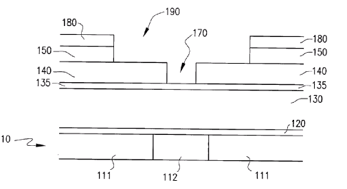
US2003207207
This place covers:
All dual damascene processes in which in an early stage a via is formed partially through the dielectric stack. The via etch is completed later in the process, e.g. during the etching step for forming the trench.
Examples:
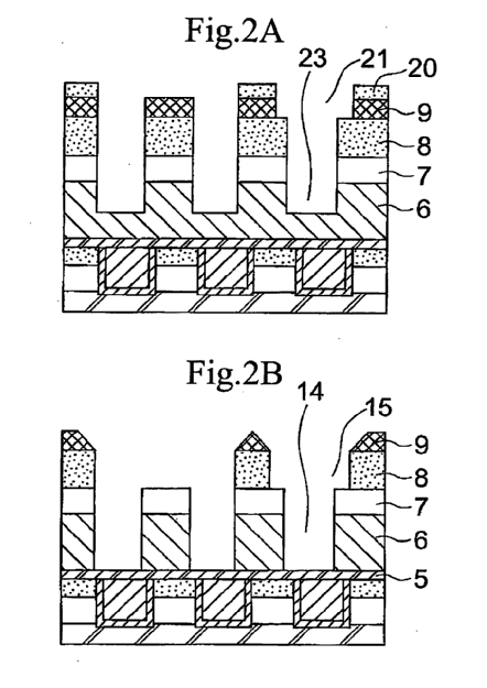 US2006166482
First, the via is partially etched into the dielectric stack. In a later step, the via etch is completed together with the trench etch.
Dual damascene processing also involving a stack of pre-patterned hard mask layers, the group symbol H01L 21/76811 is also assigned.
If the partial via process also includes a step of intermediate filling the partial via with a planarising material, the document needs to be classified in H01L 21/76808, too.
This place covers:
Particular method steps designed for improving the result of a process of forming an interconnect opening in a dielectric, e.g. removal of oxides from the surface of a conductor at the bottom of a via hole, removal of etching residues, or treatments restoring the dielectric at the sidewalls.
Examples:
After formation of the opening 10, the photoresist mask and etch residues are removed using a reducing plasma. During this treatment an undesired coating layer 14 forms on the sidewalls of opening 10. Layer 14 is eventually removed by the directional beam of charged oxidizing particles having its main axis 20 parallel to the sidewalls of opening 10:
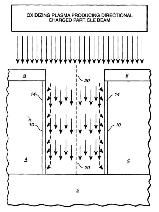 US6673721
Note that in this case the sidewall layer 14 is an undesired by-product of a plasma treatment process. The document should therefore not be classified in H01L 21/76831.
After forming an opening in a low-k dielectric, a degassing treatment and a plasma treatment are carried out in order to remove methyl groups from the dielectric and an oxide from the underlying conductor 22A:
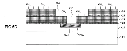
 US2005272247
This place does not cover:
After-treatment steps leading to the formation of modified sidewall layers |
If the method of after-treatment comprises aspects which are classified in any one of the subgroups H01L 21/76822+ (see below), the corresponding group should also be given. If the after-treatment leads to the formation of a sidewall layer in the opening comprising modified dielectric material, the group H01L 21/76831 should also be assigned (note, however, that if the sidewall insulation is formed by a conventional deposition step, H01L 21/76831 is the only relevant group).
H01L 21/76814 is essentially a multistep group, i.e. the after treatment step is only one of several steps to be carried out in order to form an interconnection. If a document exclusively relates to cleaning of openings in dielectrics (in a single-step fashion), the main group symbol is H01L 21/02063.
This place covers:
The geometrical "aspects" to be classified in this group are mainly methodological aspects, e.g. step sequences leading to a reduction of the pitch between via holes, step sequences for incorporating a plurality of vias of different depth, methods of forming vias having a particular cross-sectional shape.
Examples:
Layer 230 is introduced into the structure to enable the simultaneous formation of a deep and a not-so-deep via. Although the formation of the vias themselves contains no special features at all, there is an aspect related "to the size of the vias":
 US2006281290
Method for decreasing the pitch between adjacent contact holes by using a sequence of steps involving among other things a sacrificial pattern (13 in the figure below) and a conformal hardmask layer (14') to create an array of vias having a pitch below what is possible by standard lithography:
 EP1818977
This place does not cover:
Geometrical aspects relating to "tapered" vias, i.e. vias having a wider part somewhere |
This place covers:
Imprinting or stamping techniques for forming openings in dielectrics.
Methods using a stamp either to pattern a mask, e.g. a resist mask, for forming the opening or to imprint the opening directly into a dielectric
Example:
 US7148142
Attention is drawn to the following places, which may be of interest for search:
Planarisation of insulating materials per se |
This place covers:
All aspects related to forming or after-treatment steps which lead to a modification of the material of a dielectric layer within an interconnection structure.
Manufacture of "graded" dielectric layers having a varying composition throughout its thickness, no matter if said grading is achieved by a modified deposition process or an after-treatment.
Examples:
Graded dielectric layer: density and permittivity characteristics vary uniformly from a top portion to a bottom portion of the layer. The variation is achieved through varying deposition parameters such as flow rate of constituent process gases or deposition chamber pressure, or through a post deposition treatment, such as plasma treatment or curing:
 US2006003598
The surface of the PSG layer 704 is made hydrophilic by a "scrubbing treatment" 710:
 US2006003582
It is not important whether the various treatment steps are conducted on a "main" interlevel or intralevel dielectric or on a "thin functional dielectric layer" as defined in H01L 21/76829 and subgroups.
If the treatment involves a patterned layer including an opening, the group H01L 21/76814 should also be given.
This place covers:
Processes designed for rendering a dielectric layer of an interconnect stack conductive
Examples:
A diamond etch-stop layer (66 in the figure below) is rendered conductive by implanting Ti followed by thermal treatment.
 US5990493
A document classified in this group is additionally classified in H01L 21/76822 and subgroups thereof, whenever appropriate, the method of conversion involves a plasma treatment, or an ion implantation.
This place covers:
After-treatment or post-treatment process of dielectric layers of the interconnect stack involving particle radiation, e.g. removal of moisture etc. by UV or e-beam radiation, processes for modifying the dielectric constant of the layer, introduction of dopants into the dielectric by particle irradiation.
Examples:
A layer of silane is deposited onto a polymer dielectric layer 16. This layer is then exposed to UV light to initiate polymerization of the silane molecules to form an adhesion promoter layer 18 (or an etch stop or hard mask layer), and to react the adhesion promoter layer with low dielectric constant polymer layer 16:
 US2005221606
The upper surface of the porous MSQ film 105 is treated by electron beam irradiation or by UV irradiation to reinforce the upper portion in the film 105:
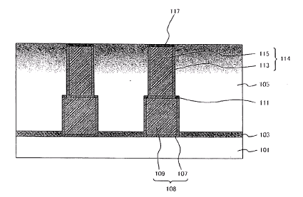 US2006211235
This place does not cover:
Removal of porogens for manufacturing porous dielectrics | |
Plasma treatment |
If the treatment is performed to form or modify a "thin functional" dielectric layer, e.g. an etch stop, one of the groups H01L 21/76829 is additionally assigned.
Curing of a dielectric precursor material is generally not considered an "after-treatment" but characterizes the formation of the dielectric layer per se, covered by H01L 21/02348.
This place covers:
Processes involving contacting a dielectric of an interconnect stack with gases, liquids or plasmas in order to modify the internal structure and/or properties of the dielectric, e.g. nitridation, removal of organic groups from the layer, introduction of dopants into the dielectric using gases, liquids or plasmas.
Examples:
a low-k dielectric is treated in a supercritical fluid after deposition, after via etching, to improve mechanical strength or repair plasma damage:
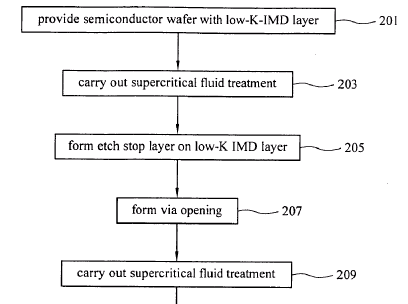 US2006073697
Plasma treatment 130 is carried out in order to decrease the C- or F- concentration in an upper layer 120a of the ILD 120:
 US2006286793
Plasma treatment is carried out in order to modify the sidewalls of a damascene opening 218:
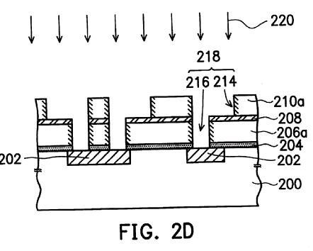 US6013581
Attention is drawn to the following places, which may be of interest for search:
Supercritical fluid treatment after a via hole formation | |
Plasma treatment is carried out to form a modified sidewall layer in an opening |
If the plasma treatment is carried out to form a modified sidewall layer in an opening, the group symbol H01L 21/76831 must also be assigned.
This place covers:
Thermal treatment for modifying the internal structure and/or properties of the dielectric of an interconnect stack, e.g. removal of moisture.
Example:
After completion of the deposition, the low-k dielectric layer 206 is subjected to a heat treatment in a nitrogen-free atmosphere to promote the out-gassing of the volatile materials 220 and especially of nitrogen and nitrogen compounds:
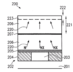 US2004121265
Attention is drawn to the following places, which may be of interest for search:
Plasma annealing |
If the heat treatment is carried out in reactive atmospheres, i.e. inevitably involves modification of the dielectric material by e.g. introducing a further chemical element into the layer, e.g. plasma annealing, the group symbol H01L 21/76826 is additionally assigned.
This place covers:
All aspects related to the formation and the geometry of so-called "thin functional dielectric layers", e.g. etch-stop films or dielectric barrier or liner layers.
Examples:
Fabrication of an oxygen-doped low-k SiC etch-stop layer 230:
 US2003085408
Nitride liner 130 imparts tensile stress in the underlying semiconductor to improve carrier mobility:
 US2005233514
Silicon oxide layer 224 is formed on top of a low-k dielectric. Layer 224 serves as a sacrificial cap layer:
 US2004121265
If a document dealing with a thin functional dielectric layer also contains after-treatment aspects as defined in H01L 21/76822+, one (or more) of the latter groups should also be assigned to this document.
In this place, the following terms or expressions are used with the meaning indicated:
"Thin" layer as used herein means thin compared with the "main" interlevel or intralevel dielectric. In cases of doubt as to whether the layer is "thin" in the above sense, the criterion "functional layer" takes precedence, i.e. documents relating to layers, which may not exactly be "thin" in the above sense but serve some particular purpose except from merely isolating conductors, should also be classified here.
This place covers:
Sidewall layers that are formed by direct deposition
Sidewall liners obtained by treatment of the sidewalls of the opening.
Examples:
Sidewalls of a porous dielectric are plasma-treated in order to form a carbon sealing layer 24 on via sidewalls 22:
 US2006046472
Non-metallic layer 15, e.g. silicon carbide or boron carbide is deposited in a dual damascene opening and etched back to form sidewall spacers 19:
 US6284657
If the treatment has characteristics relating to any of the groups H01L 21/76822+, one (or more) of the latter groups should also be assigned.
This place covers:
Stacks of two or more thin "functional" dielectric layers, e.g. multiple etch stop layers, multiple trench liners.
Examples:
Composite adhesion/etch-stop multilayer (SiC layer 104 and SiOC layer 106) is formed; layer 104 is for improving adhesion between layers 100 and 106:
 US2006110912
Multiple dielectric capping layers 616/622 and 620/624 are formed by gas cluster ion beam "infusion":
 WO2006052958
In this place, the following terms or expressions are used with the meaning indicated:
"multiple" | two or more layers in direct contact with each other. |
This place covers:
Insulating film covering some part of the conductor regardless of whether the conductor is "free-standing" or an inlaid conductor.
Example:
Dielectric film 107 covers the top and part of the sidewalls of inlaid conductors 105:
 US2005087871
Temporary sacrificial encapsulation layer (206 in fig. 5, 306 in fig. 6) is formed in a dual damascene opening and covering an exposed underlying conductor in order to form a protective layer for subsequent cleaning steps:
 US2006292863
This place does not cover:
Dielectric sidewall liners in openings |
This place covers:
Dielectric layer stacks in which e.g. the via-level dielectric and the trench-level dielectric comprise different low-k materials or in which e.g. the structure contains a low-k etch-stop or adhesion layer separating two dielectrics of which at least one must be a low-k dielectric.
Examples:
Trench-level dielectric (spin-on low-k dielectric 24) and via-level dielectric (CVD SiOC layer 10) are different low-k materials:
 US2005130407
Via-level and trench-level dielectrics (204 and 212) are made of the same low-k material, but the etch-stop layer 206 is made of a different low-k material:
 US2005263876
Posts (40) are made of a non-porous low-k dielectric whereas the material filling the spaces between the posts is a porous low-k dielectric:
 US2005227480
This place does not cover:
Middle etch-stop layer being a multilayer system |
This place covers:
Special measures for improving the gap-filling properties of a dielectric, wherein said "gap" is formed between conductive structures. The term "gap" is also intended to include vertical gaps.
Example:
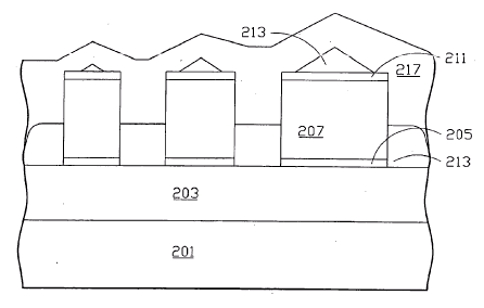 US2005186796:
a first dielectric (213) is deposited over conductive structures 207 and etched back (the figure above shows the layer 213 after etch-back) so as to partially fill the gap and reduce its aspect ratio, a second dielectric (217) fills the remaining gap.
Attention is drawn to the following places, which may be of interest for search:
When the interconnect is also used as the conductor part of a conductor-insulator-semiconductor electrode (gate level interconnections) | |
Etching for patterning conductors |
Information peculiar to single-step processes should also be classified in the corresponding group(s), e.g.
- H01L 21/02041 for cleaning;
- H01L 21/3213 for etching;
- H01L 21/321 for planarising, etc.
This place covers:
Thin conductive film being formed in an opening in a dielectric, e.g. barrier, adhesion, nucleation, seed or liner layers.
Example:
a barrier layer comprising e.g. Ru, Ir etc. or one of their (conducting) oxides is deposited in a trench or a dual damascene opening:
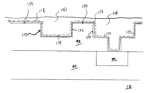 US2005206000
Attention is drawn to the following places, which may be of interest for search:
Thin films serving as seed layer for electroplating |
All documents dealing with the formation of thin conductive films in openings should be classified in this group or one of its subgroups even if the fact that the thin film is formed in an opening is not an important aspect of the disclosure under consideration.
If the deposition method of the thin functional layer is disclosed in some detail (PVD, CVD, ALD, plating etc.), the corresponding groups H01L 21/28512 - H01L 21/2885 should also be assigned.
This place covers:
At least one of the conductive thin films in the opening does not cover the bottom of the opening in its entirety, i.e. even when the thin film is removed from only a part of the bottom of the openings.
Examples:
a set of conductive barrier layers is deposited over the sidewalls of a porous dielectric and subsequently removed from the via floor by sputtering:
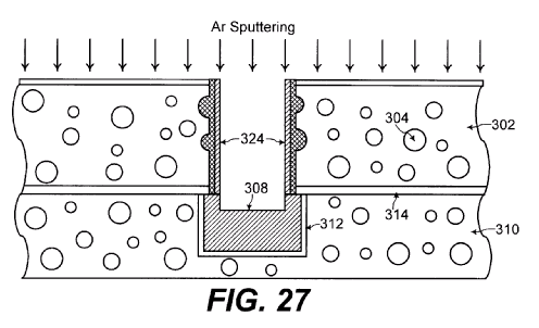 US6528409
Barrier layers covering only part of the sidewalls:
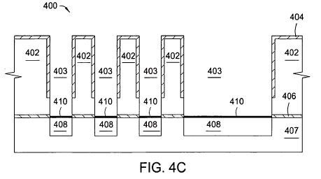 US2006246699
Multiple liner layers (30, 31, 33, 35) are deposited in a via of which only the outermost layers (30, 31) are removed from the via bottom:
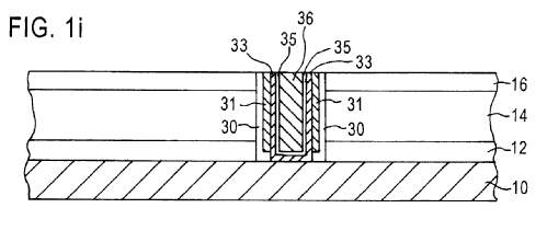 US6555461
This place covers:
Layer combinations, i.e. arrangements of more than one layer, in the openings, e.g. combinations of particular materials other than the "standard" barrier combinations Ti/TiN, TaN/Ta or W/WN.
Superlattices comprising a multitude of layers comprising "standard" materials (Ti/TiN, TaN/Ta or W/WN), e.g. a TaN/Ta/TaN/Ta... superlattice.
Graded layers, e.g. a stack of infinitely thin multiple layers with varying composition.
Conductive thin film having a graded composition
Layer combinations formed on top of an inlaid conductor
In these cases the thin film is still considered as being formed "in an opening of a dielectric", see the further explanation and example (i) under point 1.4 below).
Examples:
43 is a TaN layer, 44 is a TaN layer having a graded content of N, 45 is an alpha-Ta layer:
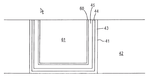 US7033940
TaN/W/TaN/W/... nanolaminates, fabricated by ALD:
 US2006079090
TaN/Ta/TaN/Ta stack:
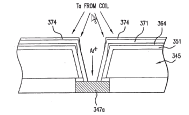 US2005255691
Different barrier materials on the sidewalls and on the bottom of the via hole (α-phase Ta layer 24 is provided on the via bottom, while the sidewalls are covered with a β-phase Ta layer 29):
 US 2004131878
This place covers:
Conductive thin film formed within the "main" conductor filling the opening or where the opening is filled by a sequence of thin films. It is important, however, that said thin film does not comprise the same material as the main fill material.
Examples:
Barrier layer 54s, 54d separates two layers of fill metal:
 US6028362
Trench filled by alternating layers 322, 324, comprising e.g. Co and Ni:
 US2006264043
This place does not cover:
Multistep plating forming a sequence of thin Cu films |
This place covers:
Conductive thin films, e.g. barrier, liner or adhesion layers, formed on top of an inlaid (i.e. damascene) conductor
Manufacture of electroless Co(Ni)WP capping layers on damascene conductors
CuSiN by siliciding and nitriding the surface of a Cu damascene conductor
Examples:
Cap layer 30 (CoWP layer) comprises multiple layers having periodic variations in the concentration of chemical elements:
 WO2006020566
Electromigration barrier formed by depositing a metal layer 11, diffusing the metal into the underlying conductor and removing the remainder of layer 11:
 WO03052798
This place covers:
Thin functional conductive films covering interconnects not formed in an opening of a dielectric, e.g. on subtractive metal lines, e.g. a Ti/TiN adhesion/barrier stack on Al wiring.
Example:
Formation of a TiN layer (141) on an Al conductor (110). The method of fabrication avoids the formation of an unintentional Ti layer (140):
 US2006099800
This place does not cover:
Barrier or adhesion layers being positioned on top of the main fill metal, e.g. thin films formed on top of inlaid conductors |
This place covers:
Barrier, adhesion or other liner layers on the sidewalls or on top and on the sidewalls of a freestanding, e.g. subtractive, interconnect.
Examples:
 US2005230262
 US 2006180920
This place covers:
Conductive thin film treated in some way after it has been deposited. The resulting film must still be a conductive film.
Attention is drawn to the following places, which may be of interest for search:
Methods of formation of barrier layers other than PVD, CVD or deposition from a liquids | |
Modifying permanently or temporarily the pattern or the conductivity of conductive members, e.g. formation of alloys, reduction of contact resistances |
This place covers:
All methods introducing a new chemical element into the thin film, e.g. the reaction of the layer with the semiconductor substrate to form a silicide.
Example:
a titanium layer (black circles in the figure below) is deposited on the sidewalls of a dielectric layer, the Ti layer reacts with the oxygen (cross-hatched circles) contained in the dielectric during a later thermal step:
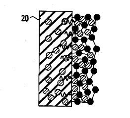 US2006214305
This place covers:
Contacting the thin film with a gas or a plasma so as to modify the composition of the layer, e.g. plasma nitriding.
Examples:
Refractive metal cap layer 303 is plasma nitrided to form a refractive metal nitride layer 305:
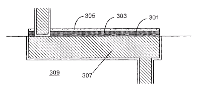 US6844258
Ru barrier layer 650b and a seed layer 666 are deposited in a trench, the seed layer is partially oxidized by exposing it to an oxidizing ambient. The oxide layer 667 serves as a protective layer and is dissolved when contacted with a plating bath:
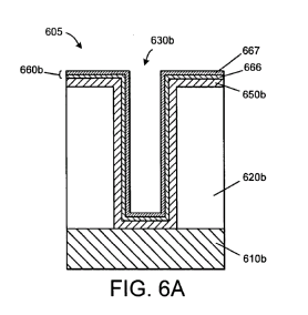 US2006223310
This place covers:
Introducing alloying elements, i.e. metallic elements, by diffusion into or reaction with pre-fabricated conductive thin film into.
Examples:
A barrier layer, an adhesion layer (Ti), a seed layer and a Cu fill are formed in a dual damascene opening; after planarisation, a thermal treatment is carried out to react the adhesion layer with the Cu thereby forming an interface layer having a graded Cu content:
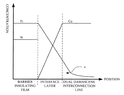 US2006154465
Conductive thin film 608 (Ca film) is formed over an inlaid Cu line (601) and heat treatment is performed to diffuse Cu from the line into the Ca layer thereby forming a CuCa capping layer (606). The unreacted material of layer 608 is subsequently removed:
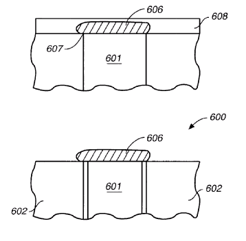 US6566262
This place does not cover:
Layers itself being fabricated by the diffusion of alloying elements |
Diffusion is a bi-directional process, i.e. there can be cases where it cannot be unambiguously determined whether the final layer is the result of diffusing elements into the layer (which would constitute an example for the present class) or if the final film is the result of diffusing elements out of an original thin film, e.g. into the bulk conductor (this would pertain to H01L 21/76867, see the examples given there). In such cases both classes H01L 21/76858 and H01L 21/76867 should be assigned.
This place covers:
Implantation methods, i.e. methods allowing for precise control of the energy of the implanted ions as well as of the implantation depth.
Examples:
Sn ions are implanted into barrier layer (440) in order to render the barrier amorphous and to introduce dopants having favourable electromigration properties:
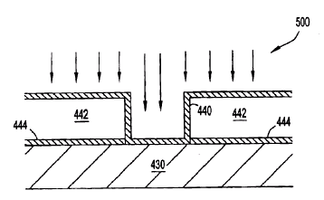 US6835655
the surface of a CoWP capping layer (34) is nitrided by N2 ion implantation:
 US2006175708
Attention is drawn to the following places, which may be of interest for search:
Implantation in semiconductors | |
implantation in insulating layers |
This place covers:
Methods for removing contaminants, e.g. oxides, from thin functional conductive films.
Methods for transforming their grain structure.
Example:
Oxides and other contaminants of a Cu seed layer (144) are removed by a wet-chemical treatment:
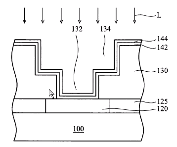 US2005245072
This place covers:
Contacting the film with plasmas or particles, e.g. high energy photons, while not introducing a new element into the film, e.g. treatment by UV irradiation for the removal of oxides.
Examples:
Barrier layer (Ti/TiN layer 118) is plasma treated to roughen the surface of the layer in the region 120. As a result, the number of nucleation sites is increased which slows down the growth of W layer 124:
 US2005014358
Barrier layer (52) is subjected to a two-step redistribution process, i.e. overhanging portions (60) are removed and redistributed to reinforce sidewall regions (32, 34) where the PVD barrier is not thick enough. In a first step, this redistribution is achieved by bombardment with Ar and Ta ions with simultaneous deposition of Ta, in the second step, only Ar is used for material redistribution:
 US2005260851
This place covers:
Thermal treatment of thin functional films not introducing additional elements into the film, e.g. plasma annealing
Examples:
a Cu seed layer (228) is locally heat treated in order to induce grain growth in the seed layer:
 US2006223311
a Ru barrier/seed layer (108) is annealed after deposition to remove oxides or other contaminants prior to plating:
 US2005274622
This place does not cover:
Film stacks, e.g. Ti/TiN and W, TaN/Ta and Cu, subjected to annealing after filling the contact hole |
Attention is drawn to the following places, which may be of interest for search:
Seed layers treated by an annealing step |
"Plasma annealing" should be classified here and in H01L 21/76862.
Note that for assigning this group symbol it is important that it is the thin film per se which is subjected to the thermal treatment. Thermal treatment of the main conductor is classified in H01L 21/76838 or, if the main conductor is formed in an opening in a dielectric, in H01L 21/76883.
Thermal treatments for driving an alloying element into the thin metal film are not classified here but in H01L 21/76858.
This place covers:
Removal of overhanging or "necking" portions of conductive thin films at the upper regions of via holes, or all cases where sputter etching and sputter deposition are carried out simultaneously.
Examples:
Seed layer (10) is removed so as to provide a base layer for selective filling of the dual damascene trench;
 US2006094220
Overhanging portions of a barrier layer 308 and/or a Cu seed layer (310) are removed and redistributed by gas cluster ion beam (GCIB) processing:
 WO2004044954
Capping layer (106) on an underlying conductor (105) is partially etched off by sputtering; the sputtered material of barrier (106) is redistributed on the via sidewalls to form a bottomless first barrier:
 US2006264030
This place does not cover:
Forming a bottomless barrier |
Attention is drawn to the following places, which may be of interest for search:
Selective removal of a seed layer for electroplating |
This place covers:
Formation of a functional conductive thin film, e.g. barrier, liner, adhesion or seed layers, by diffusing alloying elements such that they segregate at the surfaces of a conductor.
Diffusion of material from an initial thin film into a surface portion of the conductor, optionally followed by the removal of said initial thin film.
Examples:
A layer stack comprising a first barrier layer (6) and a metal layer (Hf, Zr, or Ti) suitable for forming an intermetallic compound with Cu is deposited in a dual damascene trench. A heat treatment forms layer (10b) comprising a compound of Cu and Hf, Zr, or Ti, while at the same time another compound layer (10a) is formed within the main conductor by diffusion of Hf, Zr, or Ti:
 EP0881673
Barrier layer sections 6a, 6b are formed by diffusing material of the barrier layer 510 into the porous dielectric 2:
 US2006154464
Al from Al layer 22 is diffused into inlaid Cu in order to form a CuAl electromigration barrier 12; the remaining unreacted Al layer is removed:
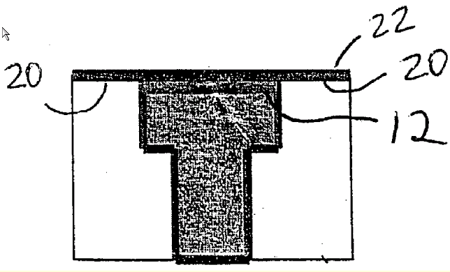 US2004207093
Attention is drawn to the following places, which may be of interest for search:
PVD | |
CVD | |
Deposition from liquids |
This place covers:
Methods specially adapted for either forming a discontinuous thin functional conductive film or for treating a discontinuous film so as to make it continuous, e.g. repair of seed layers.
Example:
Ti layer 126 is formed only incompletely on the sidewalls of contact hole 124; the TiSix layer 132 repairs the discontinuities in layer 126:
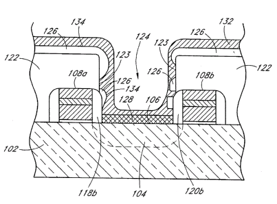 US2005233577
This place covers:
Thin conductive films formed in conjunction with the manufacture of contacts for capacitors
Example:
Formation of the barrier layer (13e):
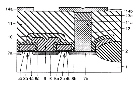 US5699291
Attention is drawn to the following places, which may be of interest for search:
Capacitor electrodes themselves |
This group is intended to sort of "filter out" all documents related to capacitor contacts providing a solution to the very specific problems encountered during the manufacture of capacitors. The groups H01L 21/76843, H01L 21/7685, H01L 21/76853, H01L 21/76867 should also be given, provided "interesting" aspects which might also be of importance in the context of more conventional barriers are disclosed.
This place covers:
Formation of seed, wetting, nucleation or catalyst layers.
Whenever any one of the structural aspects covered by H01L 21/76843 or H01L 21/7685 applies the corresponding group symbol should be given in addition to the seed layer groups with the only exception that "layer combinations", i.e. structures containing stacks of seed layers, are not classified in H01L 21/76846.
Whenever any one of the after-treatment or manufacturing aspects covered by H01L 21/76853, H01L 21/76867 or H01L 21/76868 applies the corresponding group should also be given.
Documents related to seed layers are classified in the head group H01L 21/76871 only if it is not clear which deposition method is envisaged or if the corresponding seed layer is suitable for all three of the deposition methods listed below.
This place covers:
Seed layers specifically adapted for facilitating the deposition of conductive films by electroless plating
Examples:
Formation of a Pd catalyst layer for electroless CoWP deposition on top of an inlaid Cu interconnect:
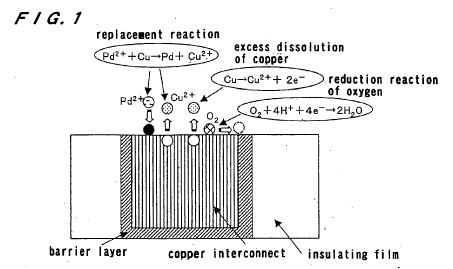 EP1496542
Formation of a Pd catalyst layer for electroless Cu plating (The Pd seed is formed by plasma-immersion ion implantation into a TaN barrier layer):
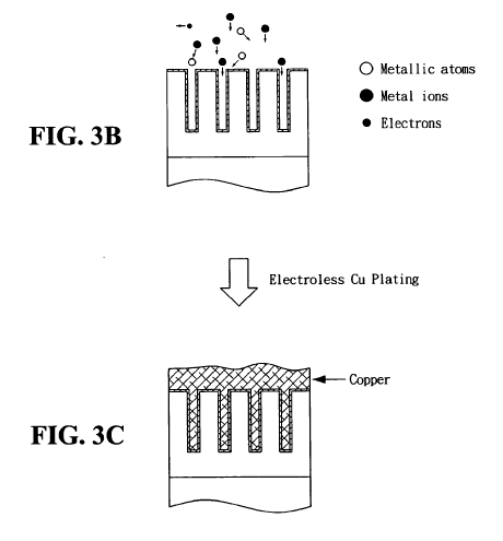 US2006040065
This place covers:
Methods for selectively filling of vias or trenches in a dielectric layer with a conductive material, e.g. bottom up fill of a damascene opening not leading to a metal overburden on the field regions surrounding the opening.
Attention is drawn to the following places, which may be of interest for search:
Plating on semiconductors in general |
If the deposition method is disclosed in some detail and includes one or more of PVD, CVD, ALD or liquid deposition, the corresponding group symbol H01L 21/2855, H01L 21/28556, H01L 21/28562, H01L 21/288 or H01L 21/2885 should also be assigned.
Attention is drawn to the following places, which may be of interest for search:
Lift-off of resists | |
Lift-off of other layers |
This place covers:
After-treatment for improving or modifying the result of the process of filling an opening in a dielectric layer, e.g. a via hole or a damascene trench, with conductive material.Thermal treatments before or after polishing, e.g. to induce grain growth, removal of metal residues, plasma cleaning
This place does not cover:
Plasma treatment specifically adapted for forming a thin layer on the surface of the conductor | |
Reflowing the conductor or applying pressure so as to better fill the opening | |
Oxidation or otherwise rendering (parts of) the conductor non-conductive |
The after-treatment is part of a multi-step process for forming a conductor in an opening in a dielectric. Cleaning of conductors per se is classified in H01L 21/02068 - H01L 21/02074.
This place covers:
Conductors formed by through-mask plating
This place does not cover:
Formation of pillars, studs, bumps etc. for connecting the semiconductor substrate to other substrates |
Attention is drawn to the following places, which may be of interest for search:
Doping |
This place covers:
Methods in which the properties of an otherwise completed conductive member of an interconnect, i.e. the main conductor, are modified, e.g. by introducing dopants into the conductor, alloying the main conductor with another metal
This place does not cover:
Smoothing; Planarisation | |
Modification of thin functional conductive films such as barrier, adhesion, liner or seed layers | |
Processes for fabricating fuses and anti-fuses are classified with the fuses and anti-fuses in |
Attention is drawn to the following places, which may be of interest for search:
Self aligned silicidation on field effect transistors |
This place covers:
Establishing a conductive path extending through the substrate from the top surface to the bottom surface, e.g. through-silicon vias
Example
 EP2426710A2
This place covers:
Processes for the division of a substrate into a plurality of individual devices.
This place does not cover:
Multistep methods for manufacturing random access memories [RAM] structures |
This place covers:
Multistep processes for singulating devices.
Attention is drawn to the following places, which may be of interest for search:
Single mechanical steps like cutting semiconductors | |
Laser dicing | |
Single mechanical steps of grinding, lapping and polishing in general | |
Fine working of crystals, e.g. semiconductors | |
Devices sensitive to light | |
Light emitting devices |
This place covers:
Separation of layers comprising active devices from the substrate, e.g. splitting after Epitaxial Lift-Off
In this place, the following terms or expressions are used with the meaning indicated:
ELO | Epitaxial Lift-Off |
This place covers:
Application of testing and/or measuring procedures during the manufacturing processes of devices as defined under H01L 21/00, with the aim to
- detect defects, repair defects, sort defective devices / wafers
- control the semiconductor device fabrication process,
- with or without corrective action on the process,
which are specific to semiconductor device fabrication, e.g. end point determination.
Covers the measuring of a single parameter or variable
Processes which are not specific to semiconductor device fabrication or processes, where the semiconductor devices are included in a larger system, are typically not classified in H01L 22/00, but are classified in the relevant place for the processes or testing in general, e.g. G01N or G01R.
Attention is drawn to the following places, which may be of interest for search:
Detecting parts, counting parts, handling parts | |
Marks on wafers, test patterns on wafers | |
Means for detecting end-point in lapping or polishing machines | |
Analysing materials by determining their chemical or physical properties | |
Optical characterization of semiconductors | |
Measuring electrical or magnetic variables | |
Multiple probes for testing, e.g. probe cards | |
Testing of individual devices, including on wafers, after manufacture | |
Testing of integrated circuits, including on wafers, after manufacture | |
Contactless testing of integrated circuits | |
Testing and controlling photoresist and lithographic patterns | |
Multiple probes for testing, e.g. probe cards | |
Inspection of images, flaw detection | |
Testing storing means, like memories, including repair | |
Measuring and control of plasma parameters | |
Controlling gas-filled discharge tubes, e.g. plasma machines, by information coming from substrate; end-point detection | |
Testing of photovoltaic systems |
This place covers:
Methods for measurement of structural or electrical parameters as part of the device manufacturing process.
Measuring as part of the manufacturing process; the parameter may be for example the thickness of layers, refractive index of layers, line width, warp of wafers, bond strength, defect concentration, metallurgic parameters, diffusion depth, dopant concentration.
Measurement of parameters wherein the fabrication of semiconductor devices is not particularly relevant to the invention, or wherein the measurement of the parameter could equally be applied to the fabrication of other products than semiconductor products are typically not classified.
This place does not cover:
Procedures, i.e. sequence of activities consisting of a plurality of measurement and correction, marking or sorting steps |
Attention is drawn to the following places, which may be of interest for search:
Measurement of parameters which is not part of the device fabrication processMeasurement of parameters wherein the fabrication of semiconductor devices is not particularly relevant to the invention, and wherein the measurement of the parameter could equally be applied to the fabrication of other products than semiconductor devices | |
Burn-in |
In H01L 22/00, the method for measuring a parameter is classified in H01L 22/20 as soon as it is part of a testing or controlling procedure.
Attention is drawn to the following places, which may be of interest for search:
Electrical measurement of diffusion regions |
This place covers:
Multi-step processes comprising at least a measuring step followed by a correcting, marking or sorting step.
This place does not cover:
Semiconductor factory control |
Attention is drawn to the following places, which may be of interest for search:
Procedures applied to semiconductor fabrication but wherein the fabrication of semiconductor devices is not particularly relevant to the invention and wherein the procedure could equally be applied to the fabrication of products other than semiconductor devices are typically classified in |
Attention is drawn to the following places, which may be of interest for search:
Voltage contrast |
Attention is drawn to the following places, which may be of interest for search:
methods for plasma etching end point control |
End point process detection, when it is exclusively based on the use of a machine which has been designed for that purpose, need not to be classified in H01L 22/00.
Attention is drawn to the following places, which may be of interest for search:
Process control influencing process steps in general, e.g. CD correction by etch or diffusion | |
Switching, multiplexing, gating devices | |
Process control with lithography, e.g. dose control | |
Structures for alignment control by optical means |
This place covers:
- Details of semiconductor or other solid state devices including
- Structural arrangements for protection of semiconductor or other solid state devices against mechanical damage or moisture
- Containers or seals
- Mountings
- Fillings or auxiliary members in containers of encapsulations
- Encapsulations
- Holders for supporting the complete device in operation
- Arrangements for cooling, heating, ventilating or temperature compensation
- Arrangements for conducting electric current to or from the solid state body in operation
- Arrangements for conducting electric current within the solid state body in operation
- Marks applied to semiconductor or other solid state devices
- Protection against radiation of semiconductor or other solid state devices
- Structural electrical arrangements for semiconductor or other solid state devices not otherwise provided for
This place does not cover:
Arrangements for connecting or disconnecting semiconductor or solid-state bodies, and methods related thereto | |
Assemblies consisting of a plurality of individual semiconductor or other solid state devices | |
Microstructural devices or systems, e.g. micromechanical devices | |
Solid state devices using organic materials as the active part, or using a combination of organic materials with other materials as the active part | |
Details peculiar to thermo-electric devices comprising a junction of dissimilar materials | |
Details peculiar to thermoelectric devices without a junction of dissimilar materials | |
Details peculiar to piezoelectric devices; electrostrictive devices; magnetostrictive devices | |
Details peculiar to devices using galvano-magnetic or similar magnetic effects | |
Details peculiar to devices using superconductivity | |
Details peculiar to solid state devices adapted for rectifying, amplifying, oscillating or switching without a potential-jump barrier or surface barrier | |
Details peculiar to bulk negative resistance effect devices |
Attention is drawn to the following places, which may be of interest for search:
Non-electric welding by applying impact or other pressure, with or without the application of heat, e.g. cladding or plating | |
Laser working of semiconductors | |
Rods, electrodes, materials, or media, for use in soldering, welding, or cutting | |
Injection moulding of electrical components | |
Optical interconnections, e.g. light guides | |
Photolithography | |
Record carriers for use with machines and containing semiconductor elements (credit cards, id cards) | |
Structure or manufacture of flux-sensitive heads using magneto-resistive devices or effects | |
Digital stores characterised by the use of particular electric or magnetic storage elements; Storage elements therefor | |
Apparatus or processes specially adapted for manufacturing, assembling, maintaining, or repairing of line connectors or current connectors or for joining electric conductors (soldering / welding) | |
Details peculiar to semiconductor devices sensitive to infrared radiation, light, electromagnetic radiation of shorter wavelength or corpuscular radiation and adapted either for the conversion of the energy of such radiation into electrical energy or for the control of electrical energy by such radiation | |
Details peculiar to semiconductor devices with at least one potential-jump barrier or surface barrier specially adapted for light emission |
The use of Indexing Codes of the indexing scheme H01L 23/00 - H01L 23/66 is mandatory for additional information.
In this place, the following terms or expressions are used with the meaning indicated:
Parts | All structural units which are included in a complete device |
Container | Enclosure forming part of the complete device and is essentially a solid construction in which the body of the device is placed, or which is formed around the body without forming an intimate layer thereon. Generally comprises a base, a lid and leads for electrical connection |
Encapsulation | Enclosure which consists of one or more layers formed on the body and in intimate contact therewith |
This place does not cover:
Mountings | |
Arrangements for cooling, heating, ventilating or temperature compensation | |
Arrangements for conducting electric current to or from the solid state body in operation | |
Protection against radiation | |
High-frequency adaptations |
Attention is drawn to the following places, which may be of interest for search:
Housings for MEMs | |
Housings for sensors in general | |
Housings for acceleration sensors | |
Housings for computers | |
Housings for record carriers, e.g. memory cards | |
Housings for memories |
This place does not cover:
The leads being parallel to the base |
Attention is drawn to the following places, which may be of interest for search:
Chip carriers per se | |
Multi-chip modules in general | |
Printed circuit boards |
Attention is drawn to the following places, which may be of interest for search:
Semiconductor conductive substrates |
This place covers:
Additional parts and fillings within container or encapsulation, e.g. stiffeners, spacing layers.
This place does not cover:
Fillings or auxiliary members in containers or encapsulations selected or arranged to facilitate heating or cooling | |
Protection against radiation |
This place does not cover:
Materials for absorbing or reacting with moisture or other undesired substances |
This place does not cover:
Materials for absorbing or reacting with moisture or other undesired substances |
This place does not cover:
Materials for absorbing or reacting with moisture or other undesired substances | |
Double encapsulation or coating and encapsulation |
This place does not cover:
Protection against radiation |
Attention is drawn to the following places, which may be of interest for search:
Insulating layers for contacts or interconnections |
This place does not cover:
Organo-silicon compounds |
Attention is drawn to the following places, which may be of interest for search:
Mask layer used as insulation layer |
This place does not cover:
Fillings of grooves in memory cells (e.g. capacitors of RAMs) |
This place does not cover:
Mountings or securing means for detachable cooling or heating arrangements |
Attention is drawn to the following places, which may be of interest for search:
Thermal treatment apparatus | |
Temperature control of computers | |
Thermal control of PCBs |
This place does not cover:
Encapsulations | |
Mountings or securing means for detachable cooling or heating arrangements | |
Fillings or auxiliary members in containers or encapsulations selected or arranged to facilitate heating or cooling | |
The complete device being wholly immersed in a fluid other than air | |
Involving the transfer of heat by flowing fluids |
Attention is drawn to the following places, which may be of interest for search:
Arrangements for heating |
This place does not cover:
Cooling arrangements using the Peltier effect | |
Mountings or securing means for detachable cooling or heating arrangements | |
Fillings or auxiliary members in containers or encapsulations selected or arranged to facilitate heating or cooling | |
Cooling arrangements with the complete device being wholly immersed in a fluid other than air | |
Cooling arrangements involving the transfer of heat by flowing fluids |
This place does not cover:
Heat sinks being part of lead-frames |
This place does not cover:
Cooling facilitated by selection of materials: diamonds | |
Cooling facilitated by selection of materials: having a heterogeneous or anisotropic structure | |
Cooling facilitated by selection of materials: laminates or multilayers | |
Cooling facilitated by selection of materials: organic materials with or without a thermoconductive filler | |
Cooling facilitated by selection of materials: semiconductor materials |
Attention is drawn to the following places, which may be of interest for search:
Diamond per se |
This place does not cover:
Cooling facilitated by selection of materials: diamonds | |
Cooling facilitated by selection of materials: organic materials with or without a thermoconductive filler |
This place does not cover:
Cooling facilitated by selection of materials: diamonds | |
Cooling facilitated by selection of materials: having a heterogeneous or anisotropic structure | |
Cooling facilitated by selection of materials: laminates or multilayers | |
Cooling facilitated by selection of materials: organic materials with or without a thermoconductive filler | |
Cooling facilitated by selection of materials: semiconductor materials |
Attention is drawn to the following places, which may be of interest for search:
Assemblies consisting of a plurality of individual semiconductor or other solid-state bodies |
Attention is drawn to the following places, which may be of interest for search:
Heating | |
Selection of materials for the device |
Attention is drawn to the following places, which may be of interest for search:
Cooling by liquefied gas |
This place does not cover:
Leadframes specifically adapted to facilitate heat dissipation |
This place does not cover:
Cooling by change of state |
This place does not cover:
Fillings or auxiliary members in containers or encapsulations selected or arranged to facilitate heating or cooling | |
Cooling arrangements with the complete device being wholly immersed in a fluid other than air |
This place does not cover:
Cooling involving the transfer of heat by flowing liquids |
This place does not cover:
Auxiliary members in containers: bellows | |
Auxiliary members in containers: pistons |
This place does not cover:
Auxiliary members in containers: in combination with jet impingement |
Attention is drawn to the following places, which may be of interest for search:
Arrangements for connecting or disconnecting semiconductor or other solid-state bodies, and methods related thereto | |
Terminals, leads in general |
Attention is drawn to the following places, which may be of interest for search:
Electrodes of semiconductor devices |
This place does not cover:
Lead-in layers inseparably applied to the semiconductor body: bridge structures with air gap | |
Lead-in layers inseparably applied to the semiconductor body: beam leads | |
Lead-in layers inseparably applied to the semiconductor body: pads with extended contours | |
Lead-in layers inseparably applied to the semiconductor body: for devices consisting of semiconductor layers on insulating or semi-insulating substrates | |
Materials | |
Bond pads | |
Bump connectors |
This place does not cover:
Bump connectors |
This place does not cover:
Leads on insulating substrates |
Attention is drawn to the following places, which may be of interest for search:
Interconnections between components using lead-frames |
This place does not cover:
Lead-frames with additional leads being a wiring board |
This place does not cover:
Lead-frames: geometry for individual devices of subclass H10D |
This place does not cover:
Lead-frames: geometry for individual devices of subclass H10D |
This place does not cover:
Thin flexible metallic tape with or without a film carrier provided in the context of subject-matter covered by groups H01L 23/49503 - H01L 23/49568 and H01L 23/49575 - H01L 23/49579 | H01L 23/49503 - H01L 23/49568 and; H01L 23/49575 - H01L 23/49579 |
Attention is drawn to the following places, which may be of interest for search:
Shape of the substrate |
This place does not cover:
Leads on insulating substrates: via connections through the substrates |
Attention is drawn to the following places, which may be of interest for search:
Multilayer metallisation on monolayer substrate |
This place does not cover:
Leads on insulating substrates: multilayer substrates | |
Leads on insulating substrates: consisting of a plurality of insulating substrates | |
Leads on insulating substrates: flexible insulating substrates | |
Leads on insulating substrates: lead-frames fixed on or encapsulated in insulating substrates |
This place does not cover:
Lead-frames consisting of thin flexible metallic tape with or without a film carrier | |
Leads on insulating substrates: for flat-cards, e.g. credit cards |
Attention is drawn to the following places, which may be of interest for search:
Cards per se |
This place does not cover:
Leads on insulating substrates: the leads being also applied on the sidewalls or the bottom of the substrate | |
Leads on insulating substrates: flexible insulating substrates |
Attention is drawn to the following places, which may be of interest for search:
Materials of the substrates | |
Materials of the lead-frames | |
Conductive materials for PCBs | H05K/09D |
Attention is drawn to the following places, which may be of interest for search:
Superconducting fullerenes |
Attention is drawn to the following places, which may be of interest for search:
For printed circuits |
This place does not cover:
Arrangements for conducting electric current to or from the solid state body in operation: lead-in layers inseparably applied to the semiconductor body | |
Leads on insulating substrates |
Attention is drawn to the following places, which may be of interest for search:
Other capacitive arrangements |
Attention is drawn to the following places, which may be of interest for search:
Other inductive arrangements |
Attention is drawn to the following places, which may be of interest for search:
Other resistive arrangements |
Attention is drawn to the following places, which may be of interest for search:
Algorithms, e.g. computer aided design of layouts of integrated circuits |
This place does not cover:
Arrangements for conducting electric current within the device in operation from one component to another: containing superconducting materials |
Attention is drawn to the following places, which may be of interest for search:
Nanosized carbon materials per se | |
Superconducting fullerenes |
Attention is drawn to the following places, which may be of interest for search:
Internal lead connections |
This place does not cover:
Printed circuits; casings or constructional details of electric apparatus; manufacture of assemblages of electrical components |
Attention is drawn to the following places, which may be of interest for search:
Manufacture or treatment | |
Mountings per se | |
Materials |
This place does not cover:
Interconnection structure between a plurality of semiconductor chips being formed on, or in, insulating substrates: assembly of a plurality of insulating substrates |
Attention is drawn to the following places, which may be of interest for search:
Multilayer metallisation on monolayer substrates |
This place does not cover:
Interconnection structure between a plurality of semiconductor chips being formed on, or in, insulating substrates: multilayer substrates | |
Interconnection structure between a plurality of semiconductor chips being formed on, or in, insulating substrates: assembly of a plurality of insulating substrates |
Attention is drawn to the following places, which may be of interest for search:
Pins attached to insulating substrates |
This place does not cover:
Interconnection structure between a plurality of semiconductor chips being formed on, or in, insulating substrates: for flat cards, e.g. credit cards |
Attention is drawn to the following places, which may be of interest for search:
Cards per se |
This place covers:
Marks for identification purposes, including electrical structures used to generate identification information for electrical read out.
Typical views of marks of this type:

Attention is drawn to the following places, which may be of interest for search:
Marking devices, scribers | |
Marking methods | |
Marks used for overlay monitoring in photolithography | |
Alignment marks used in photolithographic machines |
This place covers:
Electromagnetic shielding arrangements; RF interference suppression.
This place does not cover:
Lead-frames: battery in combination with a lead-frame | |
Lead-frames: oscillators in combination with a lead-frame |
This place covers:
Active and passive measures to prevent or detect tampering; reverse engineering protection structures; seal rings, protection against delamination of layers during dicing
This place does not cover:
Protection against electrostatic charges or discharges | |
Protection against overvoltage | |
Impedance arrangements | |
High-frequency adaptations |
Attention is drawn to the following places, which may be of interest for search:
Secure housings for data carriers (memories) | |
Protective means for data carriers (memories) |
Attention is drawn to the following places, which may be of interest for search:
Faraday shields in general | |
Protection against electrostatic discharge (ESD) provided in a semiconductor body |
This place does not cover:
Lead-frames: capacitor integral with or on the lead-frame | |
Impedance arrangements: inductive arrangements | |
Impedance arrangements: resistive arrangements | |
High-frequency adaptations |
Attention is drawn to the following places, which may be of interest for search:
Capacitive effects between wiring layers on the semiconductor body |
This place does not cover:
Impedance arrangements: resistive arrangements | |
High-frequency adaptations |
Attention is drawn to the following places, which may be of interest for search:
Inductors formed within interconnection layers |
This place does not cover:
Protection against overvoltage | |
High-frequency adaptations |
This place covers:
Examples of first level interconnects

1 = H01L 24/10 and subgroups,
2 = H01L 24/26 and subgroups,
3 = H01L 24/26 and subgroups,
4 = H01L 24/42 and subgroups
This place does not cover:
Manufacture or treatment of parts | |
Assemblies of semiconductor devices | |
Applying interconnections to be used for carrying current between separate components within a device | |
Containers or seals | |
Mountings | |
Arrangements for cooling, heating, ventilating or temperature compensation | |
Arrangements for conducting electric current | H01L 23/48 - H01L 23/50 and H01L 23/52 - H01L 23/5389 |
Structural electrical arrangements | |
Assemblies consisting of a plurality of individual semiconductor or other solid state devices | |
Printed circuits | |
Apparatus or manufacturing processes for printed circuits | |
Details peculiar to solid state devices using organic materials as the active part, or using a combination of organic materials with other materials as the active part | |
Details peculiar to thermoelectric devices comprising a junction of dissimilar materials | |
Details peculiar to thermoelectric devices without a junction of dissimilar materials or of thermomagnetic devices | |
Details peculiar to piezoelectric, electrostrictive, magnetostrictive devices in general | |
Details peculiar to devices using galvano-magnetic or similar magnetic effects | |
Details peculiar to devices using superconductivity | |
Details peculiar to solid state devices adapted for rectifying, amplifying, oscillating or switching without a potential-jump barrier or surface barrier or of Ovshinsky-effect devices | |
Details peculiar to bulk negative resistance effect devices |
Attention is drawn to the following places, which may be of interest for search:
Details of semiconductor bodies or electrodes of semiconductor devices adapted for rectifying, amplifying, oscillating or switching, or capacitors or resistors with at least one potential-jump barrier or surface barrier | |
Details peculiar to semiconductor devices sensitive to infrared radiation, light, electromagnetic radiation of shorter wavelength or corpuscular radiation and adapted either for the conversion of the energy of such radiation into electrical energy or for the control of electrical energy by such radiation | |
Details peculiar to semiconductor devices with at least one potential-jump barrier or surface barrier specially adapted for light emission |
The use of Indexing Codes of the indexing schemes H01L 24/00 and subgroups, H01L 2224/00 and subgroups and H01L 2924/00 and subgroups is mandatory.
This place covers:

Attention is drawn to the following places, which may be of interest for search:
Bonding areas on insulating substrates, e.g. chip carriers |

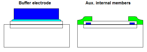
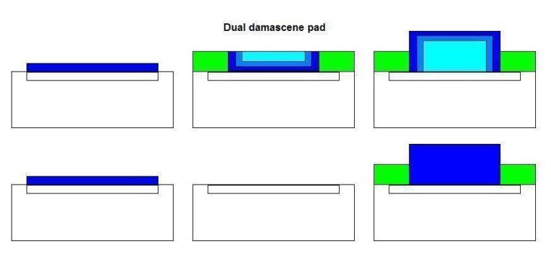
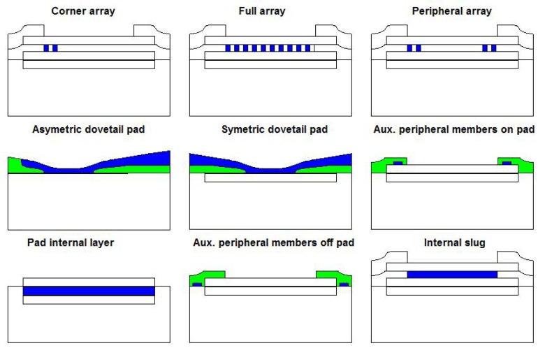
Attention is drawn to the following places, which may be of interest for search:
Physical circuit design |
In this place, the following terms or expressions are used with the meaning indicated:
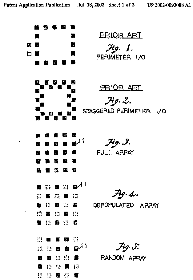
Attention is drawn to the following places, which may be of interest for search:
Bumps on insulating substrates, e.g. chip carriers |
This place covers:
![]()


Attention is drawn to the following places, which may be of interest for search:
Manufacturing methods for bumps on insulating substrates | |
Inks, e.g. metallic inks |
This place covers:

Attention is drawn to the following places, which may be of interest for search:
Interconnection structure between a plurality of semiconductor chips |
This place covers:

Attention is drawn to the following places, which may be of interest for search:
metal powder in organic matrix |
Attention is drawn to the following places, which may be of interest for search:
Applying fluids in general | |
Applying adhesive films using preforms |
This place covers:
Attention is drawn to the following places, which may be of interest for search:
Thin flexible metallic tape with or without a film carrier | |
Flexible insulating substrates |
Attention is drawn to the following places, which may be of interest for search:
Holders for supporting the complete device in operation H01L 23/32 |
This place covers:


This place covers:
![]()
Attention is drawn to the following places, which may be of interest for search:
Interconnection structure between a plurality of semiconductor chips |
Attention is drawn to the following places, which may be of interest for search:
Wire bonding in general |

This place covers:
![]()
This place does not cover:
Panels or arrays of photo electrochemical cells | |
Devices consisting of a plurality of solid state components formed in or on a common substrate | |
Photovoltaic modules or arrays of photovoltaic cells |
Attention is drawn to the following places, which may be of interest for search:
Assemblies of semiconductor devices on lead-frames | |
Leads on insulating substrates (chip carriers) | |
Interconnection structures for a plurality of bare semiconductor chips provided on or in an insulating substrate | |
Arrangements for connecting or disconnecting semiconductor or solid-state bodies; methods related thereto | |
Couplings of light guides with optoelectronic elements | |
Static Stores | |
Generators using solar cells or photovoltaic modules | |
Details of complete circuit assemblies provided for in another subclass, e.g. details of television receivers, see the relevant subclass, e.g. H04N | |
Details of assemblies of electrical components in general | |
Tandem solar cells, meaning monolithically integrated solar cells with different wavelengths sensibilities deposited on one another by coating processes | |
Integrated photodetecting devices on a substrate | |
Light sensitive devices structurally associated with, e.g. formed in or on a common substrate with, one or more electric light sources, and electrically or optically coupled thereto (e.g. opto-couplers) | |
Organic light emitting devices [OLEDs] | |
Integration of organic light emitting devices (OLEDs), e.g. OLED displays |
The classification of additional information is mandatory in this main group.
In this place, the following terms or expressions are used with the meaning indicated:
Assembly of a Device | The "assembly" of a device is the building up of the device from its component constructional units and includes the provision of fillings in containers. |
This place covers:
Arrays of photodetectors disposed next to one another on a common substrate.
This place does not cover:
Assemblies of thin film solar cells |
Attention is drawn to the following places, which may be of interest for search:
Multicolour imagers having a stacked structure | |
Multispectral infrared imagers, having a stacked structure |
In this place, the following terms or expressions are used with the meaning indicated:
Disposed | means that photodetectors already manufactured are individually placed on the common substrate, as opposed to "integrated" which means the devices are all formed on or in said substrate during the same process |
This place covers:
Photodetectors mechanically stacked on one another:
Attention is drawn to the following places, which may be of interest for search:
Light sources using semiconductor devices as light-generating elements, e.g. using light-emitting diodes [LED] or lasers |
This place covers:
Hybrid modules of active and passive components
This place does not cover:
Interconnections for hybrid circuits |
This place covers:
Arrangement of memory and logic chips
Arrangement of diode and IGBT
Attention is drawn to the following places, which may be of interest for search:
Devices consisting of a plurality of semiconductor or other solid-state components formed in or on a common substrate and controlled by radiation |
This place covers:
Processes to fabricate devices formed of an assembly of a multiplicity of components on a host substrate.
This place does not cover:
Assembly of semiconductor devices using processes or apparatus not provided for in a single one of the subgroups H01L 21/18 - H01L 21/326 |
Attention is drawn to the following places, which may be of interest for search:
Manufacturing methods of bonding areas for connecting semiconductor or solid-state bodies | |
Manufacturing methods of bump connectors for connecting semiconductor or solid-state bodies | |
Manufacturing methods of layer connectors for connecting semiconductor or solid-state bodies |
Attention is drawn to the following places, which may be of interest for search:
Amplifiers per se |
Attention is drawn to the following places, which may be of interest for search:
Passive two-terminal components without a potential-jump or surface barrier for integrated circuits |
Attention is drawn to the following places, which may be of interest for search:
Devices consisting of a plurality of semiconductor or other solid-state components comprising only passive thin-film or thick film elements formed on a common insulating substrate |
Attention is drawn to the following places, which may be of interest for search:
Antennas per se |
Attention is drawn to the following places, which may be of interest for search:
Hot-dipping or immersion processes for applying the coating material in the molten state without affecting the shape |
Attention is drawn to the following places, which may be of interest for search:
Hot-dipping or immersion processes for applying the coating material in the molten state without affecting the shape |
Attention is drawn to the following places, which may be of interest for search:
Manufacture or treatment of semiconductor parts, e.g. containers, prior to assembly of the devices using processes not provided for in a single one of the subgroups H01L 21/18 - H01L 21/326 |
Attention is drawn to the following places, which may be of interest for search:
Thermal post-treatment of the bonding area, e.g. reflowing |
Attention is drawn to the following places, which may be of interest for search:
Material with principal constituent being glasses, e.g. amorphous oxides, nitrides or fluorides |
Attention is drawn to the following places, which may be of interest for search:
Glass ceramics, e.g. amorphous oxides, nitrides or fluorides |
Attention is drawn to the following places, which may be of interest for search:
Glass ceramics, e.g. amorphous oxides, nitrides or fluorides |
Attention is drawn to the following places, which may be of interest for search:
Glass ceramics, e.g. amorphous oxides, nitrides or fluorides |
Attention is drawn to the following places, which may be of interest for search:
Glass ceramics, e.g. amorphous oxides, nitrides or fluorides |
Attention is drawn to the following places, which may be of interest for search:
Glass ceramics, e.g. amorphous oxides, nitrides or fluorides |
Attention is drawn to the following places, which may be of interest for search:
Glass ceramics, e.g. amorphous oxides, nitrides or fluorides |
Attention is drawn to the following places, which may be of interest for search:
Glass ceramics, e.g. amorphous oxides, nitrides or fluorides |
Attention is drawn to the following places, which may be of interest for search:
Layout of bonding areas prior to the connecting process |
Attention is drawn to the following places, which may be of interest for search:
Hot-dipping or immersion processes for applying the coating material in the molten state without affecting the shape |
Attention is drawn to the following places, which may be of interest for search:
Hot-dipping or immersion processes for applying the coating material in the molten state without affecting the shape |
Attention is drawn to the following places, which may be of interest for search:
Manufacture or treatment of semiconductor parts, e.g. containers, prior to assembly of the devices using processes not provided for in a single one of the subgroups H01L 21/18 - H01L 21/326 |
Attention is drawn to the following places, which may be of interest for search:
Thermal post-treatment of the bump connector, e.g. reflowing |
Attention is drawn to the following places, which may be of interest for search:
Glass ceramics, e.g. amorphous oxides, nitrides or fluorides |
Attention is drawn to the following places, which may be of interest for search:
Glass ceramics, e.g. amorphous oxides, nitrides or fluorides |
Attention is drawn to the following places, which may be of interest for search:
Glass ceramics, e.g. amorphous oxides, nitrides or fluorides |
Attention is drawn to the following places, which may be of interest for search:
Glass ceramics, e.g. amorphous oxides, nitrides or fluorides |
Attention is drawn to the following places, which may be of interest for search:
Glass ceramics, e.g. amorphous oxides, nitrides or fluorides |
Attention is drawn to the following places, which may be of interest for search:
Glass ceramics, e.g. amorphous oxides, nitrides or fluorides |
Attention is drawn to the following places, which may be of interest for search:
Glass ceramics, e.g. amorphous oxides, nitrides or fluorides |
Attention is drawn to the following places, which may be of interest for search:
Glass ceramics, e.g. amorphous oxides, nitrides or fluorides |
Attention is drawn to the following places, which may be of interest for search:
Layout of bump connectors prior to the connecting process |
Attention is drawn to the following places, which may be of interest for search:
Hot-dipping or immersion processes for applying the coating material in the molten state without affecting the shape |
Attention is drawn to the following places, which may be of interest for search:
Hot-dipping or immersion processes for applying the coating material in the molten state without affecting the shape |
Attention is drawn to the following places, which may be of interest for search:
Manufacture or treatment of semiconductor parts, e.g. containers, prior to assembly of the devices using processes not provided for in a single one of the subgroups H01L 21/18 - H01L 21/326 |
Attention is drawn to the following places, which may be of interest for search:
Thermal post-treatment of the layer connector, e.g. reflowing |
Attention is drawn to the following places, which may be of interest for search:
Layer connector being at least partially embedded in the surface |
Attention is drawn to the following places, which may be of interest for search:
Glass ceramics, e.g. amorphous oxides, nitrides or fluorides |
Attention is drawn to the following places, which may be of interest for search:
Glass ceramics, e.g. amorphous oxides, nitrides or fluorides |
Attention is drawn to the following places, which may be of interest for search:
Glass ceramics, e.g. amorphous oxides, nitrides or fluorides |
Attention is drawn to the following places, which may be of interest for search:
Glass ceramics, e.g. amorphous oxides, nitrides or fluorides |
Attention is drawn to the following places, which may be of interest for search:
Glass ceramics, e.g. amorphous oxides, nitrides or fluorides |
Attention is drawn to the following places, which may be of interest for search:
Glass ceramics, e.g. amorphous oxides, nitrides or fluorides |
Attention is drawn to the following places, which may be of interest for search:
Glass ceramics, e.g. amorphous oxides, nitrides or fluorides |
Attention is drawn to the following places, which may be of interest for search:
Glass ceramics, e.g. amorphous oxides, nitrides or fluorides |
Attention is drawn to the following places, which may be of interest for search:
Layout of layer connectors prior to the connecting process |
Attention is drawn to the following places, which may be of interest for search:
Glass ceramics, e.g. amorphous oxides, nitrides or fluorides |
Attention is drawn to the following places, which may be of interest for search:
Glass ceramics, e.g. amorphous oxides, nitrides or fluorides |
Attention is drawn to the following places, which may be of interest for search:
Glass ceramics, e.g. amorphous oxides, nitrides or fluorides |
Attention is drawn to the following places, which may be of interest for search:
Glass ceramics, e.g. amorphous oxides, nitrides or fluorides |
Attention is drawn to the following places, which may be of interest for search:
Glass ceramics, e.g. amorphous oxides, nitrides or fluorides |
Attention is drawn to the following places, which may be of interest for search:
Glass ceramics, e.g. amorphous oxides, nitrides or fluorides |
Attention is drawn to the following places, which may be of interest for search:
Glass ceramics, e.g. amorphous oxides, nitrides or fluorides |
Attention is drawn to the following places, which may be of interest for search:
Glass ceramics, e.g. amorphous oxides, nitrides or fluorides |
Attention is drawn to the following places, which may be of interest for search:
Glass ceramics, e.g. amorphous oxides, nitrides or fluorides |
Attention is drawn to the following places, which may be of interest for search:
Glass ceramics, e.g. amorphous oxides, nitrides or fluorides |
Attention is drawn to the following places, which may be of interest for search:
Glass ceramics, e.g. amorphous oxides, nitrides or fluorides |
Attention is drawn to the following places, which may be of interest for search:
Glass ceramics, e.g. amorphous oxides, nitrides or fluorides |
Attention is drawn to the following places, which may be of interest for search:
Glass ceramics, e.g. amorphous oxides, nitrides or fluorides |
Attention is drawn to the following places, which may be of interest for search:
Glass ceramics, e.g. amorphous oxides, nitrides or fluorides |
Attention is drawn to the following places, which may be of interest for search:
Glass ceramics, e.g. amorphous oxides, nitrides or fluorides |
Attention is drawn to the following places, which may be of interest for search:
Glass ceramics, e.g. amorphous oxides, nitrides or fluorides |
Attention is drawn to the following places, which may be of interest for search:
Glass ceramics, e.g. amorphous oxides, nitrides or fluorides |
Attention is drawn to the following places, which may be of interest for search:
Glass ceramics, e.g. amorphous oxides, nitrides or fluorides |
Attention is drawn to the following places, which may be of interest for search:
Glass ceramics, e.g. amorphous oxides, nitrides or fluorides |
Attention is drawn to the following places, which may be of interest for search:
Unsoldering; Removal of melted solder or other residues |
Attention is drawn to the following places, which may be of interest for search:
Electron-beam welding or cutting |
Attention is drawn to the following places, which may be of interest for search:
Material of the bonding area prior to the connecting process |
Attention is drawn to the following places, which may be of interest for search:
Glass ceramics e.g. amorphous oxides, nitrides or fluorides |
Attention is drawn to the following places, which may be of interest for search:
Glass ceramics, e.g. amorphous oxides, nitrides or fluorides |
Attention is drawn to the following places, which may be of interest for search:
Glass ceramics, e.g. amorphous oxides, nitrides or fluorides |
Attention is drawn to the following places, which may be of interest for search:
Glass ceramics, e.g. amorphous oxides, nitrides or fluorides |
Attention is drawn to the following places, which may be of interest for search:
Detachable connecting means consisting of mechanical auxiliary parts connecting the device, e.g. pressure contacts using springs or clips |
Attention is drawn to the following places, which may be of interest for search:
Unsoldering; Removal of melted solder or other residues |
Attention is drawn to the following places, which may be of interest for search:
Electron-beam welding or cutting |
Attention is drawn to the following places, which may be of interest for search:
Material of the bump connector prior to the connecting process |
Attention is drawn to the following places, which may be of interest for search:
Glass ceramics, e.g. amorphous oxides, nitrides or fluorides |
Attention is drawn to the following places, which may be of interest for search:
Glass ceramics, e.g. amorphous oxides, nitrides or fluorides |
Attention is drawn to the following places, which may be of interest for search:
Glass ceramics, e.g. amorphous oxides, nitrides or fluorides |
Attention is drawn to the following places, which may be of interest for search:
Glass ceramics, e.g. amorphous oxides, nitrides or fluorides |
Attention is drawn to the following places, which may be of interest for search:
Detachable connecting means consisting of mechanical auxiliary parts connecting the device, e.g. pressure contacts using springs or clips |
Attention is drawn to the following places, which may be of interest for search:
Electron-beam welding or cutting |
Attention is drawn to the following places, which may be of interest for search:
Unsoldering; Removal of melted solder or other residues |
Attention is drawn to the following places, which may be of interest for search:
Electron-beam welding or cutting |
Attention is drawn to the following places, which may be of interest for search:
Core member material of the layer connector prior to the connecting process | |
Coating material of the layer connector prior to the connecting process |
Attention is drawn to the following places, which may be of interest for search:
Glass ceramics, e.g. amorphous oxides, nitrides or fluorides |
Attention is drawn to the following places, which may be of interest for search:
Glass ceramics, e.g. amorphous oxides, nitrides or fluorides |
Attention is drawn to the following places, which may be of interest for search:
Glass ceramics, e.g. amorphous oxides, nitrides or fluorides |
Attention is drawn to the following places, which may be of interest for search:
Glass ceramics, e.g. amorphous oxides, nitrides or fluorides |
Attention is drawn to the following places, which may be of interest for search:
Electron-beam welding or cutting |
Attention is drawn to the following places, which may be of interest for search:
Glass ceramics, e.g. amorphous oxides, nitrides or fluorides |
Attention is drawn to the following places, which may be of interest for search:
Glass ceramics, e.g. amorphous oxides, nitrides or fluorides |
Attention is drawn to the following places, which may be of interest for search:
Glass ceramics, e.g. amorphous oxides, nitrides or fluorides |
Attention is drawn to the following places, which may be of interest for search:
Glass ceramics, e.g. amorphous oxides, nitrides or fluorides |
Attention is drawn to the following places, which may be of interest for search:
Electron-beam welding or cutting |
Attention is drawn to the following places, which may be of interest for search:
Manufacturing of interconnections to be used for carrying current between separate components with a device formed through a semiconductor substrate |
Attention is drawn to the following places, which may be of interest for search:
Apparatus for supporting or gripping semiconductor using temporarily an auxiliary support |
Attention is drawn to the following places, which may be of interest for search:
Testing or measuring during manufacture or treatment | |
Testing electrical properties or locating electrical faults |
Attention is drawn to the following places, which may be of interest for search:
Printed circuits |
Attention is drawn to the following places, which may be of interest for search:
The bump connector connecting between a semiconductor or solid-state body and an item not being a semiconductor or solid-state body, the item being metallic |