CPC Definition - Subclass H10F
This place covers:
Inorganic semiconductor devices that are sensitive to infrared radiation, visible light, ultraviolet radiation, x-ray radiation, gamma radiation or corpuscular radiation, and which are specially adapted for either the conversion of the radiation energy into electrical energy or for the control of electrical energy by such radiation.
This includes the following kinds of devices:
- Photovoltaic devices that convert light into electricity, e.g. photovoltaic cells or photovoltaic modules;
- Radiation-sensitive devices that control the flow of current through the device, e.g. photodiodes or phototransistors.
This place also covers processes and apparatus specially adapted for the manufacture or treatment of such devices.
In this subclass, infrared radiation includes far infrared radiation having wavelengths between about 700 nm and about 1 mm.
In this subclass, the periodic system used is the I to VIII Group system indicated in the Periodic Table under Note (3) of section C.
Attention is drawn to the following places, which may be of interest for search:
Production of heat using solar heat | |
Measurement of x-ray radiation, gamma radiation, corpuscular radiation or cosmic radiation with semiconductor devices | |
Measurement of radiation intensity with resistance detectors | |
Measurement of neutron radiation with semiconductor detectors | |
Couplings of light guides with optoelectronic elements | |
Obtaining energy from radioactive sources | |
Semiconductor radiation-sensitive devices that comprise organic active materials |
In this place, the following terms or expressions are used with the meaning indicated:
chip | a piece of a wafer or a substrate that has been processed to contain devices therein or thereon. The expression "diced chip" refers to the result of dicing a wafer or a substrate into a plurality of chips, whereas "undiced chip" refers to a chip before dicing or with no dicing. |
device | an electric circuit element (e.g. diode, transistor, LED, etc.); (depending on the context) can also refer to an integrated device (e.g. CMOS-IC, DRAM device, etc.). A device may be in the form of a bare or packaged chip. |
dopant | the atoms or compounds added to a material during doping |
doping | the intentional addition of a small quantity of atoms or compounds into a material to achieve a desired characteristic, e.g. to produce an n-type or p-type material |
individual | refers to: an electric circuit element not being an integrated device; or a component of an integrated device. Examples of individual devices include: diodes, transistors, photovoltaic cells, Josephson-junction devices, light-emitting diodes [LED], organic LEDs or a single LED component within an integrated device. |
integrated device | a device consisting of a plurality of semiconductor or other solid-state electric circuit elements formed in or on a common substrate |
integrated circuit | an integrated device where all the electric circuit elements (e.g. diodes, transistors, LEDs, etc.) are formed in or on a common substrate, including interconnections between the elements |
component | an electric circuit element (e.g. diode, transistor, LED, etc.) that is one of a plurality of elements formed in or on a common substrate, e.g. in an integrated device |
wafer | this can be one of the following: (a) a slice of semiconductor or electric solid-state active material. For example: a slice of silicon; a slice of a semiconducting compound, e.g. gallium nitride [GaN]; a slice of lithium tantalate [LiTaO3] for superconductor applications. (b) a multilayered laminate, having at least one layer of semiconductor or electric solid-state active material, the layer being meant to be processed into devices. For example: silicon-on-insulator [SOI]; silicon-on-glass [SOG]; silicon-on-sapphire [SOS]; a composite wafer comprising silicon carbide [SiC] on polycrystalline silicon [Si] support; a layer of semiconducting nanowires on glass. A wafer is typically processed by (e.g.) deposition, etching, doping or diffusion, and is then typically diced into chips. |
body | the region of semiconductor (resp. solid-state) material(s) within which, or at the surface of which, the physical effects that are characteristic of the device occur, and any bordering semiconductor (resp. solid-state) material(s) that are contiguous with this region. Examples: in a field-effect transistor [FET], the physical effects occur in the channel region between the source and the drain. The semiconductor body includes the channel region, the source and drain regions, and any contiguous semiconductor material; in a light-emitting diode [LED], the physical effects occur at a junction of active semiconductor layers. The semiconductor body includes these active semiconductor layers and any contiguous semiconductor layers, such as buffer layers, possibly a growth substrate, etc., that are between the cathode and anode electrodes; in a thermoelectric device, the solid-state body includes all solid-state materials in the path of current between the electrodes. |
electrode | a conductive region in or on the semiconductor body or solid-state body of a device (and other than the body itself) which exerts an electrical influence on the body, irrespective of whether or not an external electrical connection is made thereto. The term covers metallic regions which exert electrical influence on the body through an insulating region (e.g. in intentional non-parasitic capacitive coupling), or inductive coupling arrangements. In a capacitive coupling arrangement, the dielectric region is regarded as part of the electrode. The overall conductive wiring may comprise multiple portions. In such a case, only the wiring portions that exert an electrical influence on the body are considered portions of the electrode. Examples: conductive layer(s) in direct physical contact with the body; conductive region(s) exerting an inductive coupling onto the body; a multilayer structure which exerts influence on the body through an insulating region, e.g. in intentional non-parasitic capacitive coupling. |
interconnection | a conductive arrangement for conducting electric current from an electrode of a circuit element to another part of the circuit. Examples include metal wirings. |
container | a solid construction in which (one or more) devices are placed, or which is formed around the devices, for forming packaged devices. A container requires a partial or total enclosure and it may also comprise a filling. |
encapsulation | an enclosure consisting of (one or more) layers, e.g. comprising organic polymers, which at least partially enclose the (one or more) devices, thereby protecting them. An encapsulation is often used to hermetically seal devices. |
field-effect | refers to semiconductor technology wherein a voltage applied to a gate electrode creates an electric field that allows for control of current near the interface of the gate and the body, e.g. to create an inversion channel between the source and drain of a MOSFET |
package | the collection of all elements, which are external to the chip, that protect the chip or connect it to another object. Package therefore covers encapsulations, containers, package substrates, interposers, heatsinks or the like. Package does not include objects at a higher system level, like circuit boards and beyond, e.g. a housing in which the circuit board is enclosed. |
unipolar | refers to semiconductor technology that primarily involves one type only of charge carrier, i.e. it involves either holes or electrons but not both |
bipolar | refers to semiconductor technology that involves multi-carrier-type operation, i.e. which simultaneously uses both electrons and holes as charge carriers |
MIS | metal-insulator-semiconductor |
MOS | metal-oxide-semiconductor |
FET | field-effect transistor |
MISFET | metal-insulator-semiconductor field-effect transistor |
TFT | thin-film transistor |
active material | material within which the physical effects that are characteristic of the device occur |
coating | one or more layers which are formed essentially conformally on and directly associated with at least a portion of the semiconductor device, e.g. having passivating or optical effects |
Group IV material | material comprising only Group IV elements, except for dopants or other impurities |
Group III-V material | material comprising only Group III and Group V elements, except for dopants or other impurities |
Group II-VI material | material comprising only Group II and Group VI elements, except for dopants or other impurities |
Group I-III-VI material | material comprising only Group I, Group III and Group VI elements, except for dopants or other impurities |
heterojunction | interface between two different materials, the difference lying in the crystal structure and/or the composition (example: p-type amorphous silicon/n-type crystalline silicon) |
homojunction | interface between materials having the same composition, the same crystal structure and different dopants or dopant concentrations |
hybrid | refers to an image sensor having two substrates that are connected together, wherein the sensing elements are in one substrate and the driving circuitry is in the other substrate |
intrinsic region or layer | semiconductor region or layer that is undoped or not intentionally doped such that electron and hole densities are approximately equal |
junction box | enclosure attached to a photovoltaic module for electrically connecting modules together |
photovoltaic cell, solar cell | photovoltaic device that converts electromagnetic radiation (e.g. light) into direct current electricity for the purpose of providing electrical energy (not for light detection purposes). It is often, but not necessarily, part of a photovoltaic module. |
photovoltaic module | assembly of multiple photovoltaic cells that are electrically connected together |
PIN, p-i-n | junction having a p-type region/intrinsic region/n-type region structure, wherein the intrinsic layer is the light-absorbing layer. Contrast with SHJ photovoltaic cells, wherein the intrinsic layer is not the light-absorbing layer. |
PN, p-n | junction having a p-type region/n-type region structure |
Silicon heterojunction [SHJ] photovoltaic cell | heterostructure comprising two silicon materials having different crystalline structure and including a very thin intrinsic interlayer therebetween, which is not the light-absorbing layer |
Schottky barrier | metal/semiconductor barrier that is non-ohmic and rectifying |
multiple-junction photovoltaic cell, tandem photovoltaic cell | photovoltaic cell comprising multiple photovoltaic subcells formed on one another to form a single integrated structure between a single pair of anode/cathode electrodes. Typically, each subcell has a different spectral sensitivity than each other. Tunnel junctions between subcells usually ensure the electrical connection and the current flow between the subcells. |
up-conversion | process wherein two or more lower energy photons are converted to a single high energy photon to be absorbed by the photovoltaic cell. Up conversion layers are electrically isolated from the photovoltaic cell and are usually between the back reflector and the photovoltaic cell. |
In patent documents, the following abbreviations are often used:
a-Si, α-Si | Amorphous silicon |
ARC, AR | Anti-reflective coating |
AZO | Aluminium-doped zinc oxide |
BSF | Back surface field |
BSR | Back surface reflector |
c-Si | Crystalline silicon |
CIS | Copper indium sulfide [CuInS2] |
CISe | Copper indium selenide [CuInSe2] |
CIGS | Copper indium gallium sulfide [CuInxGa1-xS2] |
CIGSe | Copper indium gallium selenide [CuInxGa1-xSe2] |
CIGSSe | Copper indium gallium sulfur-selenide [CuIn1-xGaxS2-ySey] |
EWT | Emitter wrap through |
FMWT | Front metal wrap through |
FTO | Fluorine-doped tin oxide |
GZO | Gallium-doped zinc oxide |
HIT | Heterojunction with intrinsic thin layer |
IBC photovoltaic cell | Interdigitated back contact photovoltaic cell |
IR | Infrared |
ITO | Indium tin oxide |
mc-Si, µc-Si | Microcrystalline silicon |
MPPT | Maximum power point tracking |
MQW | Multiple quantum well |
MWT | Metal wrap through |
PERL photovoltaic cell | Passivated emitter rear locally-diffused photovoltaic cell |
Poly-Si | Polycrystalline silicon |
PV | Photovoltaic |
QW | Quantum well |
TCO | Transparent conducting oxide |
UV | Ultraviolet |
This place covers:
Individual inorganic photovoltaic devices that convert electromagnetic radiation (e.g. light) into direct current electricity for the purpose of providing electrical energy (not for light detection purposes). Such devices are often, but not necessarily, part of a photovoltaic module.
This place does not cover:
Electrolytic light-sensitive devices, e.g. dye-sensitized photovoltaic cells |
Attention is drawn to the following places, which may be of interest for search:
Integrated devices, or assemblies of multiple devices, comprising at least one device covered by H10F 10/00 | |
Individual radiation-sensitive semiconductor devices in which radiation controls the flow of current through the devices, e.g. photodetectors; Integrated devices or assemblies thereof | |
Manufacture or treatment of photovoltaic cells | |
Constructional details of photovoltaic cells, e.g. electrodes or coatings | |
Production of heat using solar radiation | |
Measurement of X-radiation, gamma radiation, corpuscular radiation or cosmic radiation with semiconductor detectors | |
Measurement of X-radiation, gamma radiation, corpuscular radiation or cosmic radiation with resistance detectors | |
Measurement of neutron radiation with semiconductor detectors | |
Couplings of light guides with optoelectronic elements | |
Arrangements for obtaining electrical energy from radioactive sources | |
Electrochemical current or voltage generators | |
PV power plants; Combinations of PV energy systems with other systems for the generation of electric power | |
Supporting structures for PV modules | |
Structural details of PV modules other than those related to light conversion | |
Components or accessories in combination with PV modules, not provided for in groups H02S 10/00 - H02S 30/00 | |
Testing of photovoltaic cells after manufacture | |
Organic photovoltaic cells | |
Testing of photovoltaic cells during manufacture |
Devices including a photovoltaic cell as a power source, wherein the document does not disclose any structural details regarding said photovoltaic cells, should not be classified in this main group.
This place covers:
Individual photovoltaic cells wherein electrodes make ohmic contact to the active region at small-area "points."
Illustrative example of subject matter classified in this place:
1a.

1b.

Figures 1a and 1b illustrate a photovoltaic cell (32) having thin, active InGaAs layer (38) formed on a bulk, inactive substrate (36). Localised point p+ and n+ regions (40) facilitate extraction of electrons and holes from the active layer through ohmic contacts.
This place does not cover:
Photovoltaic cells having Schottky potential barriers |
Attention is drawn to the following places, which may be of interest for search:
Electrodes |
This place covers:
Individual photovoltaic cells wherein the potential barrier consists of a metal-insulator-semiconductor (MIS) structure.
Illustrative example of subject matter classified in this place:

The Figure illustrates a photovoltaic cell having a MIS structure comprising metallic second electrodes, a thin insulator layer, and a semiconductor (208).
Attention is drawn to the following places, which may be of interest for search:
Photodetectors having a conductor-insulator-semiconductor structure |
This place covers:
Individual photovoltaic cells wherein the absorbing region or layer has a varying bandgap.
Illustrative example of subject matter classified in this place:
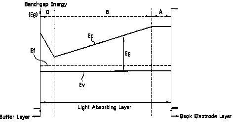
The Figure illustrates a bandgap diagram, wherein the bandgap energy Eg of a CIGSS light absorbing layer (30) is varying in region B, which is caused by adjusting the concentration of gallium or sulfur.
This place covers:
Individual photovoltaic cells wherein the potential barrier is a PN junction wherein the p-type and n-type regions are made out of one single material (i.e. having the same composition and the same crystal structure).
Illustrative example of subject matter classified in this place:

The Figure illustrates a photovoltaic cell having a PN homojunction wherein the p-type layer and the n-type layer are made of the same material and have different dopants.
Attention is drawn to the following places, which may be of interest for search:
Photovoltaic cells having PN heterojunction barriers, e.g. a-Si/c-Si photovoltaic cell | |
Photodetectors having PN homojunction structure | |
Manufacturing or treatment of photovoltaic cells |
This place covers:
Individual photovoltaic cells having multiple subcells between a single set of anode/cathode electrodes, wherein the subcells each have PN homojunctions.
Illustrative example of subject matter classified in this place:

The Figure illustrates a tandem photovoltaic cell (10) having three subcells (20, 40 and 60) that are connected in series between a pair of anode/cathode electrodes (top metal contact [14] and bottom metal contact [68]). Subcell (20) comprises GaInP regions, subcell (40) comprises GaInAs regions, and subcell (60) comprises Ge regions.
Group H10F 10/142 covers arrangements wherein subcells are formed monolithically on one another so as to form a single integrated structure. Different photovoltaic cells mechanically stacked on one another, not integrated as a single structure, are covered by H10F 19/40.
Attention is drawn to the following places, which may be of interest for search:
Tandem photovoltaic cells having PN heterojunctions | |
Tandem photovoltaic cells having PIN junctions | |
Tandem photovoltaic cells comprising subcells having a different kind of potential barrier | |
Photovoltaic cells laterally integrated on a common substrate | |
Assemblies of multiple different photovoltaic cells, wherein the cells are mechanically stacked on one another, not integrated as a single structure |
Attention is drawn to the following places, which may be of interest for search:
Heterojunction photovoltaic cells made of Group III-V materials |
This place covers:
Individual photovoltaic cells wherein the junction is a PN structure involving two different materials (i.e. having different composition or crystal structures).
Attention is drawn to the following places, which may be of interest for search:
Photodetectors having PN heterojunctions | |
Active materials of the semiconductor bodies |
This place covers:
Individual photovoltaic cells having multiple subcells between a single set of anode/cathode electrodes, wherein the subcells each have PN heterojunctions.
Attention is drawn to the following places, which may be of interest for search:
Tandem photovoltaic cells having PN homojunction barriers | |
Tandem photovoltaic cells having PIN junction barriers | |
Tandem photovoltaic cells comprising sub-cells each having a different kind of potential barrier | |
Photovoltaic cells laterally integrated on a common substrate | |
Assemblies of multiple different photovoltaic cells, wherein the cells are mechanically stacked on one another, not integrated as a single structure |
This place covers:
PN heterojunction photovoltaic cells wherein the heterojunction barrier material consists of a heterojunction between crystalline and amorphous materials.
The PN heterojunction may comprise a thin intrinsic buffer layer between the p-type and n-type layers, provided that the intrinsic layer is not the light-absorbing layer.
Illustrative example of subject matter classified in this place:

The Figure illustrates a SHJ photovoltaic cell comprising a heterojunction between n-type crystalline silicon layer (1) and amorphous silicon layers (2 and 3).
Photovoltaic cells having an intrinsic layer are classified in either H10F 10/166 or in H10F 10/17, based on the properties of the intrinsic layer. H10F 10/17 covers photovoltaic cells wherein the intrinsic layer is the layer where light is absorbed, whereas H10F 10/166 covers photovoltaic cells wherein the intrinsic layer is a thin buffer layer and is not the layer where light is absorbed.
For example, a photovoltaic cell having a PIN structure wherein the intrinsic layer is composed of an amorphous sublayer and a microcrystalline sublayer, wherein both sublayers are absorption layers, is classified in H10F 10/17.
This place covers:
PN heterojunction photovoltaic cells wherein the heterojunction barrier includes at least one Group I-III-VI material, e.g. cadmium sulfide/copper indium selenide [CdS/CuInSe2].
This place covers:
Photovoltaic cells wherein the potential barrier consists of a PIN structure, wherein the intrinsic layer is the major light-absorbing layer. For example, amorphous silicon PIN photovoltaic cells or perovskite photovoltaic cells having only inorganic active materials.
Illustrative example of subject matter classified in this place:

Photovoltaic cells having an intrinsic layer are classified in either H10F 10/166 or in H10F 10/17 based on the properties of the intrinsic layer. H10F 10/17 covers photovoltaic cells wherein the intrinsic layer is the layer where light is absorbed, whereas H10F 10/166 covers photovoltaic cells wherein the intrinsic layer is a thin buffer layer and is not the layer where light is absorbed.
For example, a photovoltaic cell wherein the intrinsic layer is composed of an amorphous sublayer and a microcrystalline sublayer, wherein both sublayers are absorption layers, is classified in H10F 10/17.
Attention is drawn to the following places, which may be of interest for search:
Photovoltaic cells having a PIN structure, wherein the intrinsic layer is a thin buffer layer and is not the light-absorbing layer | |
Photodetectors having a PIN structure | |
Radiation-sensitive devices comprising a PIN structure having at least one organic active material |
This place covers:
Individual photovoltaic cells having multiple subcells, wherein the subcells each have PIN junction barriers.
Attention is drawn to the following places, which may be of interest for search:
Tandem photovoltaic cells comprising subcells having different kinds of potential barriers | |
Photovoltaic cells laterally integrated on a common substrate | |
Assemblies of multiple different photovoltaic cells, wherein the cells are mechanically stacked on one another, not integrated as a single structure | |
Photodetectors having a PIN structure |
Attention is drawn to the following places, which may be of interest for search:
Photodetectors with Schottky structure |
For classification purposes, the Schottky metal is to be considered as part of the junction as well as part of the electrode.
Attention is drawn to the following places, which may be of interest for search:
Tandem photovoltaic cells having only PN homojunction barriers | |
Tandem photovoltaic cells having only PN heterojunction barriers | |
Tandem photovoltaic cells having only PIN junction barriers |
This place covers:
Integrated devices, or assemblies of multiple devices, comprising at least one photovoltaic cell, e.g. photovoltaic arrays, modules or panels. This includes configurations, dispositions or shapes of the photovoltaic cells in the integrated devices or assemblies.
Attention is drawn to the following places, which may be of interest for search:
Constructional details specific to photovoltaic modules | |
Supporting structure for photovoltaic modules | |
Frame structures of photovoltaic modules | |
Optical components in combination with photovoltaic modules | |
Electrical components in combination with photovoltaic modules | |
Thermal components in combination with photovoltaic modules |
In patent documents, the following words/expressions are often used as synonyms:
- "modules", "panels"
This place covers:
Photovoltaic cells formed in a bulk semiconductor substrate either having a plurality of vertical junctions or having junctions that are at least partly in V-shaped grooves.
Illustrative examples of subject matter classified in this place:
1.
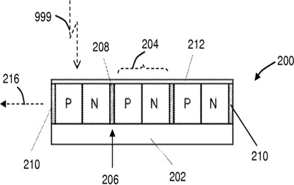
Figure 1 illustrates photovoltaic cells (204) formed on substrate (202), the photovoltaic cells (204) having vertical PN junctions.
2.

Figure 2 illustrates photovoltaic cell (66) comprising layers GaAlAs layers (72, 74 and 76), and photovoltaic cell (60) comprising Si intrinsic layers between GaP n-type and p-type layers. Both cells are both formed on substrate (62). The subcells of (66) are separated by V-shaped grooves that have been etched into the GaAlAs layers (72, 74 and 76). The subcells of (60) are separated by V-shaped grooves that have been etched into the Si layer.
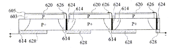
This place covers:
Photovoltaic cells in arrays in or on a single semiconductor substrate, the cells having planar junctions. Often, the cells each comprise a portion of the semiconductor substrate and a layer that is thereon, using the portion of the semiconductor substrate for its electrical properties.
Illustrative examples of subject matter classified in this place:
1a.
1b.

Figures 1a and 1b illustrate an array of photovoltaic cells (620), each having a PN junction between n-type layer (605) and p-type layer (603). The n-type layer (605) was formed by doping the top of a semiconductor layer (603). Trenches are etched between adjacent cells, and SiO2 isolation regions (614) isolate the cells within the substrate (601). Electrical connections between the cells may be made by connective wire (626) and conductive vias (624) to electrically connect the cells in series in an array configuration in photovoltaic module (650).
2a.

2b.

Figures 2a and 2b illustrate photovoltaic cells (52) on a substrate (54) in side-view (top picture) and in top-view (bottom picture). The photovoltaic cells have p-type GaAs layers (58) and n-type GaAs layers (56) that form PN junctions (60). The cells form a monolithically integrated microarray (50).
This place does not cover:
Photovoltaic modules composed of a plurality of thin film photovoltaic cells deposited on the same substrate |
This place covers:
Integrated devices or assemblies including inorganic thin-film photovoltaic cells, e.g. single thin film a-Si, CIS or CdTe photovoltaic cells.
The group H10F 19/30 itself covers an assembly of multiple photovoltaic cells, each formed on its own substrate and interconnected. The groups indented under H10F 19/30 cover integrated devices.
Illustrative example of subject matter classified in this place:

The Figure illustrates a photovoltaic cell (110) comprising PV layer (112) on its own substrate (114) and another photovoltaic cell (120) comprising PV layer (122) on its own substrate (124). The photovoltaic cells (110 and 120) are connected together and electrically connected in series by a conductive via (116).
This place covers:
Integrated devices including multiple inorganic thin-film photovoltaic cells deposited on the same substrate. Typically, the substrate is insulating and the cells do not use the substrate for its electrical properties.
Illustrative example of subject matter classified in this place:
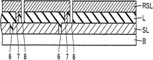
The Figure illustrates integrated thin film photovoltaic cells formed of surface electrode SL, semiconductor layer L and rear surface electrode RSL connected in series through contact line (7).
Attention is drawn to the following places, which may be of interest for search:
Thin films deposited on metallic or insulating substrates |
This place covers:
Specific patterning methods (like laser trimming, chemical etching) which aims at forming a module from a plurality of (interconnected) adjacent thin film photovoltaic cells from initially continuous thin films.
Attention is drawn to the following places, which may be of interest for search:
Processes or apparatus specially adapted for the manufacture or treatment of PV cells | |
Processes or apparatus specially adapted for the manufacture or treatment of PV cells comprising amorphous semiconductor materials |
This place covers:
Structures related to the interconnecting of adjacent thin film photovoltaic cells. Examples include interconnections and insulating spacers that prevent short-circuits between cells.
Illustrative examples of subject matter classified in this place:
1.

Figure 1 illustrates thin-film based photovoltaic cells (200a) each having absorber layers (260), buffering layers (250), transparent electrode layer (230), and back electrode layer (240), which are sandwiched between first substrate (210) and second substrate (220). Adjacent photovoltaic cells (200a) are electrically isolated by isolative layer (340) and electrically interconnected by a film of conductive paste (290).
2.

Figure 2 illustrates adjacent photovoltaic cells [1126] (1) and [1126] (2) formed on substrate (1102), wherein the adjacent photovoltaic cells are electrically interconnected by a conductive via (1128) and a conductive grid (1124).
This place covers:
Means for obtaining partial light transmission through the integrated device or the assembly.
Illustrative example of subject matter classified in this place:
The Figure illustrates light transmitting through the photovoltaic device (2) through openings (6).
This place covers:
Photovoltaic cells stacked, one on top of the other, each having their own electrodes.
Illustrative example of subject matter classified in this place:

The Figure illustrates an integrated device having two photovoltaic cells formed in a stacked configuration on top of a glass substrate (219). The bottom photovoltaic cell (230) has its own electrodes (211 and 217). The top photovoltaic cell has its own electrodes (203 and 209).
This place covers:
Photovoltaic cells integrated or directly associated with one or more electric components in or on the same substrate. Examples include a photovoltaic cell being used as an energy source to drive other semiconductor devices such as a transistor.
Illustrative examples of subject matter classified in this place:
1.

Figure 1 illustrates a device (100) comprising a p-type substrate (110) and an n-type region (112) that define a PN junction of a photovoltaic cell. Transistors and/or other circuit devices (116) are formed in or on the epitaxial layer (111) formed on a front surface of the substrate (110), enabling self-powering of the circuitry portion by the photovoltaic cell portion.
2.

Figure 2 illustrates a solar-powered self-contained integrated device (200) comprising photovoltaic cells (200a) integrated with, and providing power to, thin film sensors and circuits (200b) on substrate (200c).
This place does not cover:
Photovoltaic modules or arrays of single photovoltaic cells comprising bypass diodes integrated or directly associated with the devices |
Attention is drawn to the following places, which may be of interest for search:
Organic photovoltaic cells |
This place does not cover:
Bypass diodes within junction boxes of PV modules |
This place covers:
Packages, or parts thereof, for protecting the photovoltaic cells in the integrated device or assembly. For example, encapsulations, laminated coatings or materials formed between adjacent photovoltaic cells.
Illustrative example of subject matter classified in this place:
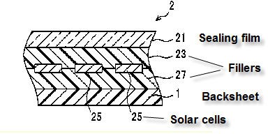
The Figure illustrates sealing film (21) and fillers (23 and 27) used to protect photovoltaic cells (25) in assembly (2).
Attention is drawn to the following places, which may be of interest for search:
Manufacture or treatment of integrated devices, or assemblies comprising at least one photovoltaic cell | |
Encapsulation of photodetectors or photodiodes | |
Layered products essentially comprising sheet glass, or glass | |
Synthetic resin laminates | |
Adhesives per se | |
Materials for sealing or packing joints or covers | |
Encapsulation of organic photovoltaic cells |
Attention is drawn to the following places, which may be of interest for search:
Layered sheets per se |
This place covers:
Means for providing the desired electrical connections between photovoltaic cells. For example, interconnections that provide a serial connection of photovoltaic cells, and insulating spacers that prevent short circuits.
Illustrative example of subject matter classified in this place:

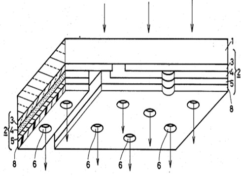
The Figure illustrates interconnections (11) that provide a serial connection of photovoltaic cells (10) in a photovoltaic module (100).
This place does not cover:
Particular structures for electrical interconnecting of adjacent thin film photovoltaic |
Attention is drawn to the following places, which may be of interest for search:
Manufacture or treatment of integrated devices, or assemblies comprising at least one photovoltaic cell | |
Electrodes | |
Soldering in general | |
Conductive pastes in general | |
Electrical interconnection means specially adapted for electrically connecting two or more photovoltaic modules |
This place covers:
Individual inorganic semiconductor devices sensitive to electromagnetic radiation or corpuscular radiation in which radiation controls the flow of current through the devices, e.g. to detect such radiation.
The group H10F 30/00 itself covers devices sensitive to corpuscular radiation and having no potential barriers. The groups indented under H10F 30/00 cover photoconductive devices or photodetectors having potential barriers.
Attention is drawn to the following places, which may be of interest for search:
Image sensors | |
Photometry | |
Pyrometry (infrared radiation measurements) | |
Sensors for corpuscular radiation, X-rays or gamma rays as a whole (including circuitry) |
In this place, the following terms or expressions are used with the meaning indicated:
photoconductive | the electrical conductivity of the material changes when light is absorbed by said material |
This place covers:
Photoconductive devices, having no junction potential barriers, which are sensitive to infrared, visible and UV light.
This place covers:
Individual inorganic semiconductor devices sensitive to electromagnetic radiation or corpuscular radiation in which radiation controls the flow of current through the devices, e.g. to detect such radiation, and comprising at least one potential barrier.
The groups indented under H10F 30/20 cover photodiodes (one potential barrier), bipolar phototransistors (two potential barriers), photothyristors (three potential barriers) and field-effect phototransistors (junction or MIS potential barriers).
Attention is drawn to the following places, which may be of interest for search:
Photovoltaic cells | |
Photoconductors | |
Photometry using radiation detectors | |
Radiation sensors (not just the photosensitive semiconducting part, but also circuitry and other aspects of sensors) | |
Semiconductor radiation intensity detectors, e.g. for very short wavelengths | |
Semiconductor neutron detector |
This place covers:
- Integrated devices comprising components in which radiation controls the flow of current through the devices. For example, integrated devices used for detection (e.g. photodiode arrays) and integrated devices used for imaging purposes (e.g. image sensors).
- Assemblies of multiple devices, comprising devices in which radiation controls the flow of current through the devices. For example, assembled photodiode arrays and assembled image sensors.
Attention is drawn to the following places, which may be of interest for search:
Individual radiation-sensitive devices in which radiation controls the flow of current through the devices | |
Integrated devices, or assemblies of multiple devices, comprising at least one organic radiation-sensitive element |
This place covers:
Manufacture or treatment of hybrid-type imagers, i.e. image sensors having two substrates that are connected together, wherein the sensing elements are in one substrate and the driving circuitry is in the other substrate.
Attention is drawn to the following places, which may be of interest for search:
Hybrid-type infrared CMOS or photodiode array image sensors | |
Hybrid-type X-ray, gamma-ray or corpuscular radiation image sensors | |
Hybrid-type infrared photoconductor image sensors | |
Constructional details of hybrid-type image sensors |
This place covers:
Manufacture or treatment of coatings (e.g. antireflective coatings, filters or shielding) or other optical elements (e.g. microlenses).
Attention is drawn to the following places, which may be of interest for search:
Coatings | |
Optical elements | |
Coatings in general | |
Lenses in general | |
Optical filters in general | |
Photonic crystals in general |
Attention is drawn to the following places, which may be of interest for search:
Optical filters | |
Waveguides | |
Cameras or camera modules with electronic image sensors | |
Control circuit arrangements for driving solid-state imagers | |
Image sensors comprising radiation-sensitive components having organic active materials |
In patent documents, the following abbreviations are often used:
APS | Active pixel sensor |
CCD | Charge coupled device |
PPS | Passive pixel sensor |
In patent documents, the following words/expressions are often used with the meaning indicated:
active pixel sensor (APS) | image sensor comprising pixel amplification means, e.g. a source follower transistor |
aperture ratio | ratio between light sensitive area of a pixel and the total area occupied by that pixel |
backside illumination | illumination of the imagers from the side of the device opposite to the imager circuitry |
blooming | spilling over of charges from one pixel to the next one after overexposure |
charge injection device | architecture of semiconductor device based on measuring currents induced in MOS capacitors at the moment charge packets are injected into the substrate |
dark current | signal generated by the image sensor when the device is in the dark |
integration time | time that an image sensor is collecting charges (photon generated and/or dark current generated) |
overflow drain | doped region to extract undesired charge resulting from blooming |
passive pixel sensor | pixels comprising only a photodiode or a photodiode and an addressing transistor without amplification |
Attention is drawn to the following places, which may be of interest for search:
Individual charge coupled devices |
In patent documents, the following words/expressions are often used with the meaning indicated:
frame-transfer CCD | two-dimensional architecture of a CCD image sensor that has an analogue memory cell for every pixel below the total array of light sensitive pixels |
full-frame CCD | two-dimensional architecture of a CCD image sensor transferring collected charge directly to readout |
interline-transfer CCD | two-dimensional architecture of a CCD image sensor wherein each photodiode has a parallel CCD storage region covered by an opaque mask. After image data has been collected and transferred to the adjacent CCD storage region charge is CCD-shifted vertically to the readout IC. |
TDI-type CCD-image sensor | time delay and integration [TDI] is a type of CCD wherein a TDI clock is used to synchronize the movement of charged packets in a CCD with that of another movement |
This place covers:
- The disposition of the elements within the pixel, such as the transfer, driving, reset transistors, capacitor or photodetector;
- the disposition of electrodes and wiring lines such as the power, bit and data lines; and
- the disposition of doped regions within the pixel.
Illustrative examples of subject matter classified in this place:
1.

Figure 1 illustrates photoelectric conversion elements (110 - 112) connected to wiring lines (106 - 108), with the disposition thereof being chosen such that the distance between the photoelectric conversion elements and the wiring lines are shifted based on pupil correction (see where [106 and 110] overlap more than [107 and 111] overlap, which overlap more than [106 and 112]).
2.

Figure 2 illustrates an image sensor having a buried photodiode (23), buried gate electrode (22) and buried floating diffusion (16) in such a geometry that that buried gate can be used to efficiently transfer charges to the buried floating diffusion through path R1 at a depth equal to that of the photodiode.
Attention is drawn to the following places, which may be of interest for search:
Circuit arrangements for driving solid state image sensors |
Attention is drawn to the following places, which may be of interest for search:
Optical shielding in general for image sensors |
This place covers:
CCD-type image sensors having a linear arrangement of the pixels, e.g. fax heads or photocopiers.
This place covers:
CCD-type image sensors having pixels arranged in a 2D matrix or in a 3D matrix.
This place covers:
CCD image sensors having a combination of interline transfer together with frame transfer.
Each photodiode has a parallel CCD region which shifts charge vertically to a storage 2D matrix (one storage pixel per one photosensitive pixel). The charges stored in the storage matrix are then read out.
Illustrative example of subject matter classified in this place:

This place covers:
CCD image sensors wherein each photodiode has a parallel CCD storage region covered by an opaque mask. After image data has been collected and transferred to the adjacent CCD storage region charge is CCD-shifted vertically to the readout IC.
Illustrative example of subject matter classified in this place:

The Figure illustrates an image sensor having columns of photo-sensitive areas adjacent to columns of storage regions (denoted "CCD registers").
This place covers:
CCD image sensor wherein a 2D storage area is adjacent to the photosensitive 2D array, having a storage pixel per photosensitive pixel. The charges collected are transferred in parallel to the storage area for readout.
Illustrative example of subject matter classified in this place:

The Figure illustrates an image sensor having a 2D storage area adjacent to a 2D photo-sensitive array.
This place covers:
CCD image sensors of the time delay and integration (TDI) type, wherein the pixel clock rate must be matched to the image velocity.
This place covers:
Charge-injection device [CID] image sensors wherein the object to be imaged is in contact with the sensor and typically use LEDs for the illumination of the object to be imaged.
This place does not cover:
CCD or CID colour image sensors | |
CCD or CID infrared image sensors |
Attention is drawn to the following places, which may be of interest for search:
Contact-type image sensors |
Attention is drawn to the following places, which may be of interest for search:
Colour image sensors having photoconductive layer |
This place covers:
Illustrative example of subject matter classified in this place:

The Figure illustrates an image sensor having stacked diodes sense blue, green and red light.
Attention is drawn to the following places, which may be of interest for search:
Infrared image sensors having photoconductive layer |
This place covers:
Hybrid image sensors for sensing infrared radiation, having two substrates that are connected together, wherein the sensing elements are in one substrate and the driving circuitry is in the other substrate.
Attention is drawn to the following places, which may be of interest for search:
Hybrid-type X-ray, gamma-ray or corpuscular radiation image sensors | |
Hybrid-type infrared photoconductor image sensors | |
Constructional details of hybrid-type image sensors | |
Interconnections |
This place covers:
Image sensors having generally a stacked structure for sensing different parts of the infrared spectrum, e.g. for sensing long-wave IR [LWIR], middle wavelength IR [MWIR] and short wavelength IR [SWIR].
Attention is drawn to the following places, which may be of interest for search:
Stacked colour imagers |
Attention is drawn to the following places, which may be of interest for search:
Blooming suppression in imagers having photoconductive layer |
Attention is drawn to the following places, which may be of interest for search:
Overflow drains in photoconductor image sensors |
Attention is drawn to the following places, which may be of interest for search:
X-ray, gamma ray or corpuscular radiation image sensors having a photoconductor layer | |
Measuring X-ray, gamma-ray or corpuscular radiation |
This place covers:
X-ray, gamma-ray or corpuscular radiation image sensor wherein the semiconductor layers directly convert the incoming radiation into charges, without need of a scintillator.
This place covers:
Hybrid image sensors for sensing X-ray, gamma-ray or corpuscular radiation, having two substrates that are connected together, wherein the sensing elements are in one substrate and the driving circuitry is in the other substrate.
Attention is drawn to the following places, which may be of interest for search:
Hybrid-type infrared CMOS or photodiode array image sensors | |
Constructional details of hybrid-type image sensors | |
Interconnections |
This place covers:
X-ray, gamma-ray or corpuscular radiation image sensors having a scintillator (e.g. an ionic solid or phosphor) which converts incoming radiation into visible light, which is then detected.
Attention is drawn to the following places, which may be of interest for search:
Measuring X-ray radiation with a scintillation-diode combination |
This place covers:
Image sensors wherein incoming radiation changes the conductivity of a photoconductive layer and the change in conductivity is measured to determine the incoming radiation.
This place covers:
Hybrid photoconductive image sensors having two substrates that are connected together, wherein the photoconductive sensing elements are in one substrate and the driving circuitry is in the other substrate.
Attention is drawn to the following places, which may be of interest for search:
Hybrid-type infrared CMOS or photodiode array image sensors | |
Hybrid-type X-ray, gamma-ray or corpuscular radiation image sensors | |
Constructional details of hybrid-type image sensors | |
Interconnections |
Attention is drawn to the following places, which may be of interest for search:
Overflow structures in photodiode array or CMOS type image sensors |
Attention is drawn to the following places, which may be of interest for search:
X-ray, gamma ray or corpuscular radiation-detecting photodiode or CMOS type image sensors | |
Measuring X-ray, gamma-ray or corpuscular radiation |
This place covers:
Image sensors having integrated light sources, wherein the light emitted from the integrated light source is reflected on the object to be detected and enters the image sensors. Examples include scanning heads, photocopier heads and fingerprint detectors.
Attention is drawn to the following places, which may be of interest for search:
Charge-injection device [CID]-type image sensors | |
Fingerprint or palmprint sensors | |
Sensors for vascular patterns | |
Scanning, transmission or reproduction of documents or the like, e.g. facsimile transmission |
This place covers:
Image sensors wherein radiation (e.g. light) impinges from the surface of the semiconductor wafer opposite to the surface having the imaging structure.
Illustrative example of subject matter classified in this place:

The Figure illustrates light (250) illuminated on the surface of the semiconductor wafer that is opposite to the surface having photodiodes (200) therein.
This place covers:
Structural or functional details of semiconductor imaging structures such as encapsulations, geometry of disposition of passive and active elements, lenses, isolation, etc., whenever they are specific for semiconductor imaging devices, i.e. they solve problems specific to semiconductor imaging devices.
Attention is drawn to the following places, which may be of interest for search:
Encapsulation of integrated circuits |
This place covers:
Illustrative example of subject matter classified in this place:

The Figure illustrates an image sensor having optical waveguides (106) having two components (106a and 106b) having differing index of refraction. In the pixels near the periphery of the image sensor, regions (106b) are large, and in the pixels near the middle of the image sensor, regions (106b) are small.
This place covers:
Illustrative example of subject matter classified in this place:

The Figure illustrates the implanted photosensitive region (432) of a photodiode having a shape (see dotted lines) determined by mask (305).
This place covers:
Pixels of active pixel sensors [APS], wherein each pixel comprises a photodetecting element and amplifications means.
Illustrative examples of subject matter classified in this place:
1a.

Figure 1a illustrates a top view of an image sensor having photoelectric conversion regions (17) of photodiodes in multiple pixels, with reset transistor (12), amplification transistor (13) and selection transistor (14) formed between rows of photodiodes.
1b.

Figure 1b illustrates a corresponding circuit diagram.
Attention is drawn to the following places, which may be of interest for search:
Scanning details of image sensors | |
Circuitry of image sensors |
This place covers:
Details of the photosensitive area of an active pixel sensor, such as doping profiles, etc.
Illustrative example of subject matter classified in this place:

The Figure illustrates a photodiode (121) comprising photosensitive regions (133 and 134C). The region (134) extends below a buried channel (135) in a way that helps prevent charge in (121) from mixing into other regions.
Attention is drawn to the following places, which may be of interest for search:
Geometry of the photosensitive area in image sensors |
This place covers:
Active pixel sensors characterised by a transistor (e.g. transfer transistor, reset transistor or source follower) in the pixel.
This place covers:
Illustrative example of subject matter classified in this place:

The Figure illustrates a flexible container (9) comprising copper (13a), adhesive (13b), and polymer (14a), that is attached to metal pads (24) of an image sensor and is wrapped therearound. It further shows an encapsulation material (30), such as epoxy, that seals the container (9) to the top of the image sensor.
Attention is drawn to the following places, which may be of interest for search:
Encapsulation of integrated circuits in general | |
Containers of integrated circuits in general |
This place covers:
Coatings within the image sensor, e.g. interlayer dielectrics (ILD) or antireflective coatings (ARC).
Illustrative example of subject matter classified in this place:

The Figure illustrates an image sensor having coatings such as a transparent film (30) having a carefully chosen apex angle such that a lens may be formed thereon by deposition of other thin films.
Attention is drawn to the following places, which may be of interest for search:
Coatings in general | |
Optical filters in general |
This place covers:
Colour filters for image sensors, e.g. arrangement of multiple filters in a Bayer pattern.
Illustrative example of subject matter classified in this place:

The Figure illustrates a colour filter (23) having blue colour filter components (2B), red colour filter components (2R) and green colour filter components (2G), in a pattern known as a Bayer array, wherein each green colour filter component is surrounded by red and blue filter components.
This place covers:
Illustrative examples of subject matter classified in this place:
1.

Figure 1 illustrates an image sensor having a light-shielding film (107) having openings (111) that are largest in peripheral region (3), that are smaller in optical black region (2), and that are smallest in effective pixel region (1).
2.

Figure 2 illustrates an image sensor having a light control film (21) having a reverse tapered opening (19) over the photoelectric conversion portion (4).
Attention is drawn to the following places, which may be of interest for search:
Shielding in CCD-type image sensors |
This place covers:
Optical elements such as lenses, reflectors or light-guiding structures within image sensors.
Attention is drawn to the following places, which may be of interest for search:
Lenses in general | |
Photonic crystals in general |
This place covers:
Illustrative example of subject matter classified in this place:

The Figure illustrates an image sensor having microlenses (204a, 204b, 104a and 104b), having different sizes than each other.
This place covers:
Elements that reflect light in the image sensor, for example reflecting light towards the light detecting elements.
Illustrative example of subject matter classified in this place:

The Figure illustrates an image sensor (110j) having reflective thin films of SiN (140) formed above photodiodes (18).
This place covers:
Electrical or thermal isolation structures between pixels.
This place covers:
Illustrative example of subject matter classified in this place:

The Figure illustrates a hybrid image sensor, having photodiodes in sensor wafer (40), connected to control circuitry in CMOS wafer (41). The details of this hybrid image sensor, such as the wafer-to-wafer interconnection (56) and the metal shield (100), are covered by this subgroup.
Attention is drawn to the following places, which may be of interest for search:
Hybrid-type infrared CCD or CID imagers | |
Hybrid-type infrared CMOS or photodiode array image sensors | |
Hybrid-type X-ray, gamma-ray or corpuscular radiation image sensors | |
Interconnections |
This place covers:
Interconnections for image sensors, e.g. wirings that connect an imaging substrate with its driving substrate; or that connect an image sensor with the external driving circuitry; or that connect between various elements within the image sensor.
Illustrative example of subject matter classified in this place:

The Figure illustrates an image sensor (100) having interconnections including wiring portions (12), conductive pillars (9) and pad portions (17).
This place covers:
Arrangements in the image sensor for transferring charges perpendicular to the imaging plane, e.g. circuitry beneath the photosensitive area that move the charges away from the sensing elements.
This place covers:
Electronic components shared by multiple pixels, e.g. transistors or doped regions shared by adjacent pixels.
Illustrative example of subject matter classified in this place:

The Figure illustrates an image sensor (31) having photodiodes PD1 through PD4 that share a floating diffusion region FD, which is connected to the gate of amplifier transistor Tr3.
This place covers:
- Integrated devices having at least one light-emitting source and at least one inorganic photodetector optically coupled thereto (e.g. optocouplers).
- Assemblies of at least one light-emitting source and at least one inorganic photodetector optically coupled thereto (e.g. optocouplers).
- Radiation-sensitive semiconductor devices being structurally associated with at least one light-emitting source and being electrically coupled thereto (e.g. image converters).
- The group H10F 55/00 itself covers situations wherein it is not specified if the light-emitting source controls the radiation-sensitive device or if the radiation-sensitive device controls the light-emitting source. Groups indented under H10F 55/00 cover when it is known which device controls the other.
Attention is drawn to the following places, which may be of interest for search:
Coupling light guides with opto-electronic elements | |
Amplifiers using electroluminescent elements or photocells | |
Electronic switching using opto-electronic devices | |
Optical interconnects | |
Electroluminescent light sources per se | |
Inorganic semiconductor devices having potential barriers being adapted for light emission | |
Integrated devices, or assemblies of multiple devices, comprising at least one organic light-emitting element and at least one organic radiation-sensitive element, e.g. organic optocoupler |
This place covers:
Devices wherein the signal from the photodetector is used for controlling the emission of light from the light source (e.g. image converters).
Illustrative example of subject matter classified in this place:

The Figure illustrates an image-converting device having a photoconductive layer (6) associated with an electroluminescent layer (12) between back electrode (7) and transparent electrode (2). Radiation into the image-converting device decreases the resistivity of the photoconductive layer (6) so that the electroluminescent layer (12) emits light by the application of an electric field.
This place covers:
Devices wherein the light from the light source is sent to the photodetector, which provides an electrical signal.
Attention is drawn to the following places, which may be of interest for search:
Proximity sensors | |
Coupling light guides with opto-electronic elements | |
Electronic switching or gating using opto-electronic devices |
This place covers:
Processes or apparatus specially adapted for the formation of semiconductor devices that are sensitive to infrared radiation, visible light, ultraviolet radiation, x-ray radiation, gamma ray radiation or corpuscular radiation, and which are specially adapted for either the conversion of the radiation energy into electrical energy or for the control of electrical energy by such radiation, having active materials that are inorganic.
This includes the formation, patterning or treatment of the inorganic materials used in active layers or in electrodes.
This place does not cover:
Patterning processes to connect thin photovoltaic cells in integrated devices, or assemblies of multiple devices, having photovoltaic cells | |
Manufacture or treatment of encapsulations or containers for integrated devices, or assemblies of multiple devices, having photovoltaic cells | |
Manufacture or treatment of integrated devices, or assemblies of multiple devices, comprising at least one element in which radiation controls the flow of current |
Attention is drawn to the following places, which may be of interest for search:
Testing of photovoltaic devices, e.g. of PV modules or single PV cells | |
Manufacture or treatment of semiconductor or solid-state devices | |
Testing of semiconductor devices (e.g. photovoltaic devices) during manufacture |
Manufacturing of packages, or parts thereof, for protecting photovoltaic cells in integrated devices or assemblies are covered in H10F 19/80.
This place covers:
Constructional details of semiconductor devices that are sensitive to infrared radiation, visible light, ultraviolet radiation, x-ray radiation, gamma ray radiation or corpuscular radiation, and which are specially adapted for either the conversion of the radiation energy into electrical energy or for the control of electrical energy by such radiation, having active materials that are only inorganic.
This place does not cover:
Constructional details of integrated devices, or assemblies of multiple devices, comprising at least one element in which radiation controls the flow of current |
Attention is drawn to the following places, which may be of interest for search:
Frame structures of photovoltaic modules | |
Optical components in combination with photovoltaic modules | |
Electrical components in combination with photovoltaic modules | |
Thermal components in combination with photovoltaic modules |
When classifying in this group, the type of device itself, when it is determined to be novel and non-obvious, should be classified in groups H10F 10/00, H10F 19/00, H10F 30/00 or H10F 55/00.
The manufacturing of the constructional details covered by this group are classified together with said constructional details. For instance, a method of fabrication of an electrode for a photovoltaic cell is classified under H10F 77/211.
Attention is drawn to the following places, which may be of interest for search:
Organic semiconductor materials in bodies of organic radiation-sensitive devices |
This place covers:
Semiconductor particles, e.g. nanoparticles, in a matrix, e.g. the matrix being made of dielectric or of semiconductor material.
This place does not cover:
Semiconductor devices including thin films |
In patent documents, the following words/expressions are often used with the meaning indicated:
MGL | Mono-grain layer, also called mono-grain membrane, i.e. powder particles embedded within a polymer membrane |
This place covers:
Thin semiconductor films on metallic or insulating substrates, e.g. glass, or ceramic substrates, often formed on barrier layers that prevent out-diffusion of impurities from the substrates.
This place covers:
One or more layers that are formed essentially conformally on, and directly associated with, at least a portion of the semiconductor device. These layers may provide passivating or optical effects.
This place does not cover:
Provisions for preventing damage caused by corpuscular radiation, e.g. for space applications |
Attention is drawn to the following places, which may be of interest for search:
Encapsulations or containers for integrated devices, or assemblies of multiple devices, having photovoltaic cells | |
Wavelength conversion means | |
Encapsulations | |
Coatings for organic photosensitive semiconductor devices |
This place covers:
Optical elements or arrangements that are associated with the radiation-sensitive device, e.g. used for focusing, reflecting or diffracting light.
This place does not cover:
Surface textures for light trapping effects |
Attention is drawn to the following places, which may be of interest for search:
Light-reflecting or light-concentrating means specially adapted for photovoltaic modules |
This place covers:
Optical elements or arrangements directly associated or integrated with photovoltaic cells, e.g. solar concentrators, lenses, reflectors or Fresnel lenses.
Illustrative example of subject matter classified in this place:

The Figure illustrates glass cover (2104), low refractive index material sheet (2116) and light guide layer (2114) stacked on photovoltaic cell (2102).
Attention is drawn to the following places, which may be of interest for search:
Antireflective coatings for light sensitive devices | |
Concentrating means for semiconductor photodetectors | |
Concentrators for solar heat collectors | |
Optical elements per se |
This place covers:
Coatings or separate members, which change the wavelengths of the incident light, making it more suitable for absorption by the photovoltaic cell, e.g. fluorescent concentrators.
Illustrative example of subject matter classified in this place:

Attention is drawn to the following places, which may be of interest for search:
Wavelength conversion means for photodetectors | |
Luminescent, e.g. electroluminescent, chemiluminescent materials |
In patent documents, the following words/expressions are often used as synonyms:
- "photoluminescent materials", "luminescent materials", "phosphorescent materials"
This place covers:
Light-reflecting means that reflects the light that already went through the photovoltaic cell back into the cell.
Attention is drawn to the following places, which may be of interest for search:
Electrodes for photovoltaic cells |
This place covers:
Encapsulations or containers, e.g. housings, transparent windows or resins, for individual radiation-sensitive devices.
This place does not cover:
Encapsulations or containers for integrated devices or assemblies of multiple devices having at least one photovoltaic cell |
Attention is drawn to the following places, which may be of interest for search:
Sealing arrangements of electroluminescent light sources | |
Packages for inorganic light emitting devices | |
Passivation, containers or encapsulations for organic radiation-sensitive devices | |
Encapsulations for organic light emitting devices | |
Encapsulations for semiconductor or solid-state devices | |
Containers for semiconductor or solid-state devices |
Attention is drawn to the following places, which may be of interest for search:
Cooling apparatuses in general, e.g. arrangement or mounting of refrigeration units | |
Means to utilise heat energy directly associated with the PV module | |
Arrangements for cooling, heating, ventilating or temperature compensation or semiconductor or solid-state devices |
Attention is drawn to the following places, which may be of interest for search:
Cooling means for PV modules | |
Thermoelectric devices operating with Peltier or Seebeck-effect only | |
Cooling means using Peltier elements for semiconductor devices in general |
Attention is drawn to the following places, which may be of interest for search:
Using solar heat per se | |
Means to utilise heat energy, the means directly associated with PV modules | |
Thermoelectric devices (e.g. Seebeck elements) per se |
This place covers:
Surface textures specially adapted for light trapping effects.
In patent documents, the following words/expressions are often used as synonyms:
- "corrugated surface", "protrusions", "projections", "roughened surface", "pyramidal structures (for silicon)", "light trapping"
This place covers:
Provisions to specially adapt photovoltaic devices for space applications or to improve the radiation resistance to avoid radiation damage.
Attention is drawn to the following places, which may be of interest for search:
Semiconductor devices sensitive to very short wavelengths, e.g. X-rays, gamma-rays or corpuscular radiation | |
Space applications, e.g. power supply for satellites made of photovoltaic cell modules |
This place covers:
Energy storage means directly associated or integrated with photovoltaic cells, e.g. batteries to store electrical energy produced by photovoltaic cells.
Attention is drawn to the following places, which may be of interest for search:
Circuit arrangements for charging batteries with photovoltaic cells | |
Energy storage means associated with the PV module |