CPC Definition - Subclass B81C
This place covers:
B81C deals with manufacturing methods of microstructures as defined in the definition statement of B81B.
Subject-matter belonging to B81C
Documents which contain one of the following characteristics should be classified in B81C:
A solution to a technical problem which is common to microstructures in general (e.g. avoiding stiction, hermetic encapsulation, fabricating structures with high aspect ratio)
A process / structure which is not specific to a given application (e.g. process for making a membrane, torsion beam not specific to a given optical switch, packages for MEMS devices, machines specific to MEMS manufacturing, stamps for making microstructure).
Examples:
documents that deal with processes that solve a general problem but mention as an example a specific application should nevertheless be classified in B81C since the invention could also be applied to other applications
Subject-matter excluded from B81C
B81C doesn't cover applications which describe processes for manufacturing pure biological or chemical material (DNA sensors, carbon nanotubes ...)
Processes for solving a problem which is specific to a kind of device like increasing the sensitivity of a pressure sensor
Limits with application classes (e.g. switches H01H 1/0036)
- If the objective problem solved by the invention is related to improving physical features of the device, or realising a given function, then the document should be classified in the application classes. For example: membrane structure for improving the sensitivity of an acceleration sensor, structure for realising a bi-stable switch, structure for increasing the oscillation frequency of an RF switch.
- If the objective problem solved by the invention is related to fabricating a specific or a general structure, or to a structure for solving a general problem, i.e. a problem that is not specific to a given device, then the document should be classified in B81C. For example: process for avoiding in-use stiction.
Limits with Microfluidic applications
Following criteria applies for classifying a document on microfluidic technology in B81C:
- The document describes a method for making a microfluidic device, the function of the device being not relevant for the manufacturing process. For example, a method (e.g. bonding stamped polymer layers) for making a three dimensional arrangement of channels and grooves.
- The document describes a process which solves a technical problem general to all kind of microfluidic devices
Following documents are not to be classified in B81C:
- Documents that describe a method for making a microfluidic structure which has a specific purpose, where the structure solves a problem specific to the technical field contemplated. For example, a specific arrangement of channels for mixing given liquids (belongs to B01F 33/30)
- Documents which describe also a manufacturing method corresponding to a microfluidic structure, while the method is not relevant to the invention (i.e. the method doesn't contribute to solve a technical problem general to the field of microfluidics).
- Documents that describe a process for solving a technical problem specific to the technical field contemplated
Limits with Nanotechnologies (B82B)
Attention is drawn to the following places, which may be of interest for search:
Actuators
Micromanipulators | |
Ink jet, Nozzles, Production of nozzles, manufacturing processes, etching, dry etching, wet etching. | |
Micropumps | |
Micropumps having electric drive having plate-like flexible members, e.g. diaphragms | |
Mechanically-driven clocks or watches; mechanical parts of clocks or watches in general N.B: Processes for making gears (in particular for clocks) are classified in B81C 99/0075+ | |
Switches making use of micromechanics; Apparatus or processes for their manufacturing, e.g. anisotropic etching (for electrostatic relays H01H 59/0009, for relays in general H01H 50/005) | |
Electrostatic relays; Electro-adhesion relays; making use of micromechanics | |
Electrostatic motors, electric motors using thermal effect | |
Electric machines using piezoelectric effect | |
Networks comprising electromechanical or electro-acoustic devices; Electromechanical resonators. Details of microelectro-mechanical resonators, Driving or detection means, Comb electrodes ... | |
Microphones, microspeakers: Electrostatic transducers using semiconductor materials | |
Piezoelectric devices (includes sensors using a piezoelectric element); Electro active polymer (EAP) actuated artificial muscles |
Sensors
Gyroscopes; Turn-sensitive devices using gyroscopic effect, e.g. using gas, using electron beam. Turn-sensitive devices with vibrating masses, e.g. tuning fork, the vibrating mass being an essentially two-dimensional body which undergoes a deformation or translation vibration in a micromechanical structure | |
Measuring volume flow or mass flow | |
IR sensor | |
Pressure sensors, manufacturing methods of pressure sensors | |
Acoustic emission sensors | |
Accelerometers, Measuring acceleration; Measuring deceleration; Measuring shock, i.e. sudden change of acceleration | |
Arrangements or instruments for measuring magnetic variables (flux or magnetic sensors) |
Optical devices
Optical switches: Optical devices or arrangements using movable or deformable optical elements for controlling the intensity, colour, phase, polarisation or direction of light, e.g. switching, gating, modulating, the reflecting element being a micromechanical device, e.g. a MEMS mirror, DMD the reflecting element being moved or deformed by electrostatic means: |
Microfluidic and chemical analysis devices or processes
Microneedles (Devices for taking blood samples by percutaneous method) | |
Microneedles (devices for introducing media into the body) N.B.: Manufacturing methods (other then plastic moulding) for making raised tips (in particular microneedles) are classified in B81C 1/00111. Methods for coating the needles with an active material for therapeutic purposes is not classified in B81 | |
Processes specially adapted for manufacturing semi-permeable membranes for separation processes or apparatus, Inorganic membrane formation (micropores) | |
Micromixers | |
Microreactors, e.g. miniaturised or microfabricated reactors | |
Containers for the purpose of retaining a material to be analysed with fluid transport, e.g. multi-compartment structures by integrated microfluidic structures, i.e. dimensions of channels and chambers are such that surface tension forces are important, e.g. lab-on-a-chip | |
Manufacturing microneedles by plastic moulding | |
Measuring or testing processes involving nucleic acids (DNA analysis) | |
Manufacture of fluid circuit elements; Manufacture of assemblages of such elements integrated circuits (microvalves) | |
Investigating or analysing materials by the use of electric, electro-chemical, or magnetic means. Electrophoresis for analysis in microdevices |
Memories
Recording by means directly associated with the tip of a microscopic electrical probe as used in Scanning Tunneling (STM) or Atomic Force Microscopy (AFM) for inducing physical or electrical perturbations in a recording medium, the permanent effect of which being the writing of at least one information unit of a sequence disposed along a track; Reproducing such memorised information by such association of tip and means; Record carriers or media specially adapted for such transducing of information - ROM with cantilevers. | |
Digital stores characterised by the use of particular electric or magnetic storage elements; Storage elements therefor, using electric elements, using ferroelectric elements (using multibit ferroelectric storage elements G11C 11/5657) | |
Digital stores characterised by movement of mechanical parts to effect storage, e.g. using balls; Storage elements therefor (storing by actuating contacts G11C 11/48) - RAM with mechanical structure | |
Magnets or magnetic bodies characterised by the magnetic materials therefor; Selection of materials for their magnetic properties. Bidimensional, e.g. nanoscale period nanomagnet arrays. | |
Read-only memory structures including field-effect components |
Micromanipulators
Micromanipulators N.B: Documents which comply with the following criteria are to be classified in B81: The micromanipulator is specific to the manipulation and assembling of micro- or nanoparts for MEMS or NEMS. The device solves the problem of surface forces being higher than the gravitational force The document describes the structure and manufacturing process of the micromanipulator. Methods for controlling the micromanipulator are to be classified in B25J 7/00 only. |
Chemistry, Nanoparticles, nanowires
Other Nanoparticles | |
Coated nanoparticles for use as PIGMENTS and/or Fillers | |
Hyperbranched macromolecules | |
Nanowires - see EP0931859 - Electrolytic coating by surface reaction, i.e. forming conversion layers | |
Single crystal growth methods of nanorods and nanowires (deposition) | |
Semi-conductor nanoparticles | |
Semi-conductor nanowires / nanotubes / whiskers | |
Nanowires as semiconductor heterojunction of materials of different groups | |
Manufacturing method for silicon nanowires / nanotubes / whiskers | |
Nanowires as interconnects for ICs |
Testing and monitoring
Measuring probes , probe needles, cantilever beams, "bump" contacts; replaceable spring loaded probe pins ; N.B: plugs, sockets or clips are in G01R 1/0408; testing of connections in G01R 31/66; contacting IC's for test purposes when probe design is not the essential feature in G01R 31/2886; using radiation beam as probe in G01R 31/302; end pieces for wires terminating in a probe in H01R 11/18 | |
Testing and control, e.g. testing of apparatus components, dose control, overlay monitoring, structures for alignment control by optical means | |
Details of semiconductor or other solid state devices, marks applied to semiconductor devices (or parts), e.g. registration marks, test patterns (alignment structures, wafer maps), using circuits for characterising or monitoring manufacturing processes, e.g. whole test die, wafers filled with test structures, on-board-devices incorporated on each die, process/product control monitors or PCM, devices in scribe-line/kerv, drop-in devices |
Apparatus for lithography
Photomechanical, e.g. photolithographic, production of textured or patterned surfaces, e.g. printing surfaces; Materials therefor, e.g. comprising photoresists; Apparatus specially adapted therefor, Apparatus for microlithography |
Others
Injection moulding (for example for microneedles) | |
Imprinting and embossing machines (EP06124007) | |
Control arrangements or circuits, of interest only in connection with visual indicators other than cathode-ray tubes no fixed position being assigned to or needed to be assigned to the individual characters or partial characters, by control of light from an independent source; Control circuit for an array of optical MEMS, for example for avoiding stiction, see SA675787 - | |
Apparatus or processes specially adapted for manufacturing or assembling transformers, inductances, reactors or choke coils, for applying magnetic films to substrates (covering metals, or materials with metals, in general C23C; manufacturing record carriers G11B 5/84), for applying nanostructures, e.g. by molecular beam epitaxy (MBE) | |
Variable MEMS capacitors |
The classification scheme in B81C comprises two kinds of classification codes:
- The codes B81C 1/00 - B81C 99/00 are the main groups which are defining technical problems solved by the teaching of the classified documents.
- The Indexing Codes B81B 2201/00 - B81B 2207/99 and B81C 2201/00 - B81C 2900/00 are defining technical features of the invention.
Accordingly, the classifier should stick as much as possible to the following rules:
- Each document to be classified in B81C should be allocated only one main group corresponding to the objective technical problem solved by the invention, unless the content of the document describes more than one invention. In case the classification does not contain a group corresponding to the technical problem, the classifier should allocate either a residual group (see below), or in exceptional cases, when appropriate, several groups that in conjunction describe the technical problem.
- As the invention may comprise several essential technical features, a document classified in B81C may be allocated more than one Indexing Code. The Indexing Codes which are allocated should be relevant to the invention.
- Furthermore, the Indexing Codes must only be allocated to documents which are receiving a main group
Residual Groups
The classification in B81C contains so called residual groups. For example:
B81C 1/00253 . . . Processes for integrating an electronic processing unit with a micromechanical structure not provided for in B81C 1/0023 - B81C 1/00246
When classifying a document which doesn't correspond to any subgroup (for example B81C 1/0023 - B81C 1/00246), the document must be classified in the residual group, if present, and not in the main group. In the present example, the documents should be classified in B81C 1/00253 and not in B81C 1/00222.
The classifier must stick to this policy: no new document should be classified in a main group if a residual group is present.
The reason for these residual groups is to provide the search examiner with the certainty, that all documents in the groups have been classified or reclassified. If a residual group is not present, but subgroups are, the examiner has no certainty that the documents from the main group have been reclassified when creating the subgroups.
When doing the search, the presence of the residual group indicates that all documents in the residual group have been classified taking into account the subgroups of the same level. Documents in the group of higher level, which have been split up into the sub-groups, may not have been classified taking into account the sub-groups.
Therefore, at search stage, the examiner must keep in mind that he must verify if documents are present in the main group, since these documents have not been reclassified.
The classification structure in B81
The classification in B81, based on IPC8, makes the difference between structures and processes. In many cases, the underlying problems, which form the basis for the technical definition of a group, are solved either with a structural solution, or with a manufacturing process. Therefore, some group descriptors are duplicated in B81B (Structures) and in B81C (Processes).
The criteria for deciding if a document is to be classified in the structures or in the process is the following:
- if the solution to the technical problem is a structure, then the document should be classified in B81B
- if the solution to the technical problem is a method, then the document belongs to B81C
Example:
B81B 3/0002 . Arrangements for avoiding sticking of the flexible or moving parts and
B81C 1/00912 . Treatments or methods for avoiding stiction of flexible or moving parts of MEMS
If for example, a document describes a process using supercritical CO2 for avoiding stiction, then it should be classified in B81C 1/00928.
If the document describes a bump for avoiding stiction of a cantilever, then it should be classified in B81B 3/001.
Exceptions:
B81B 3/0005 contains also the processes for making anti-stiction coatings
In this place, the following terms or expressions are used with the meaning indicated:
Many technical terms in MEMS technology are defined in the SEMI norm SEMI MS3-0307. In the following sections, some technical expressions are given an additional explanation in the meaning of the classification scheme.
Summary of static and elastic structures:
Defined by their geometry
Extending structures | Pillar / ColumnTip |
Depressed structures | Cavity GrooveHole |
Stiction | Unintended adhesion of a moving part to another part |
Suspended structures | Bridge Cantilever Diaphragm See-saw Comb structure |
Defined by their function
Extending structures | AnchorRib |
Depressed structures | ChannelNozzle |
Suspended structures | Flexure Membrane Spring Torsion hingeProof mass |
Summary of Rotating elements
Rotating elements | Gears Rack and pinionHinge |
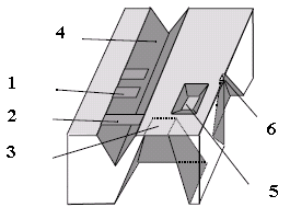
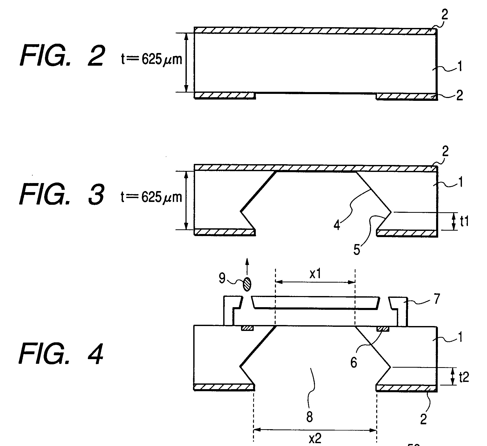
Figure 1: Basic structures
1) Cantilever 2) Bridge 3) Diaphragm 4) V-Groove 5) Well/Cavity
6) Hole/Nozzle, [1]
Pillar/Column B81B 2203/0361 | A tall vertical structure, usually narrow in proportion to its height, which is usually used as a support structure, anti-adhesion structure or a structure for thermal exchange. |
Tip | Tips are small pointed or rounded structures often used for Scanning Probe Microscopy probes (SPM) - like atomic force microscope (AFM), but also for data storage (Millipede), electron tunnelling tip (used in sensors) or microneedles. |
Bump | It is a raised structure similar to a tip. It is generally used to describe the raised structures used for avoiding stiction of movable parts. It is also used in relation to structures for reducing adhesion. |
Functional layers | Functional layers are used mostly as protective coatings. They can protect structures against chemical or mechanical corrosion that can release particles into the protected cavity. Special coatings are used also to prevent adhesion of movable structures or to reduce the stress. Metallic layers covering polymer sealing are used to make them hermetic, but can be used also to compensate the RF-interferences. |
Anchor B81B 2203/0307 | Anchors are structures connecting the suspended movable parts to the substrate. They can affect the resonant frequency and the reliability of the device. |
Rib | Stiffening ribs are may be used to improve the stiffness of suspended structures. Improving the stiffness to mass ratio, they can have impact on resonant frequency and efficiency of the devices. |
Cavity B81B 2203/0315 | In bulk micromachining, cavity is used to make the movement of a suspended element possible. It can be used also for the protection of movable structures in packaging, for thermal insulation or as a container for fluids (see Figure 1). The synonyms are chamber, hollow, well. |
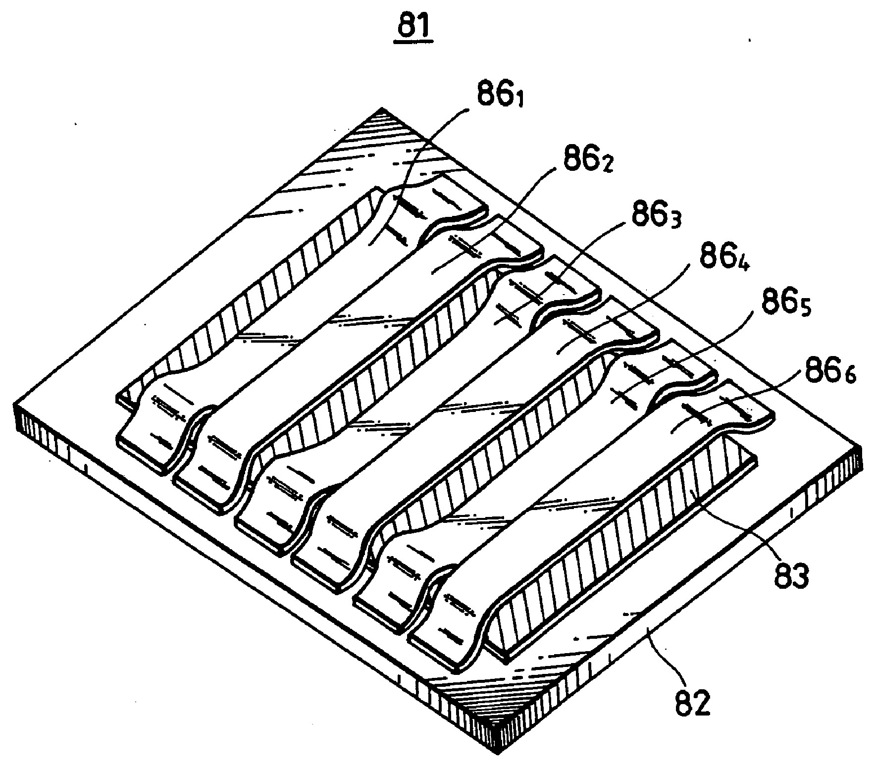
Groove B81B 2203/0346 | A typical example is a V-Groove (see Figure 1), which can be formed in 100 - Si substrate by KOH etching. Sometimes the groove in 111 - Si substrate is called channel or trench to distinguish them, but we consider channel to be a function oriented definition. Grooves are usually used in microfluidic applications, but can also be used for precise positioning of optical fibres or controlled weakening of structures holding a device prior to its separation by breaking. |
Hole B81B 2203/0353 | An aperture passing through anything, a perforation, opening. |
Channel B81B 2203/0338 | A tube or tubular passage, natural or artificial, usually for liquids or fluids. |
Nozzle | A spout, mouthpiece, projecting aperture, or a short terminal pipe from which a jet of gas or liquid may issue or be discharged (see Figure 1). |
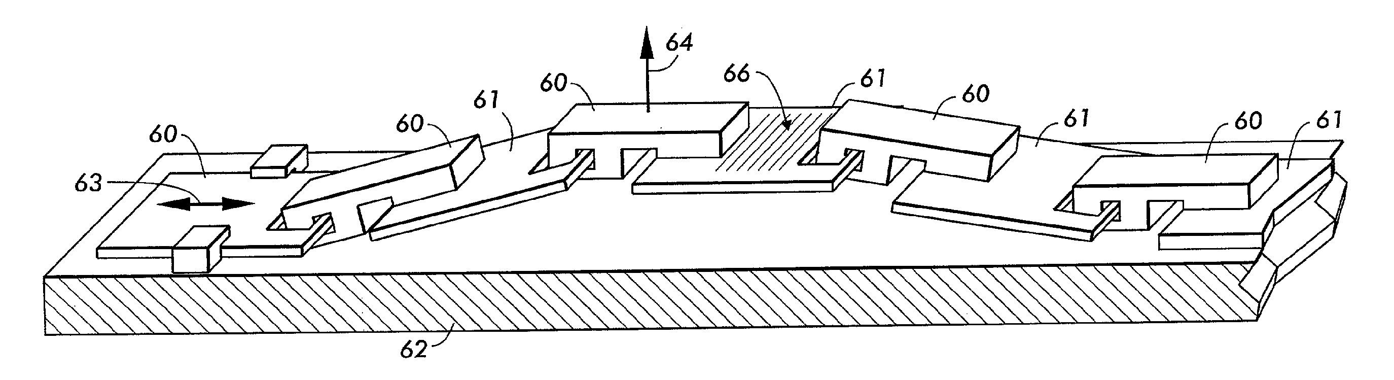
Bridge B81B 2203/0109 | A bridge is a structure, erected or suspended over a surface, depression or an obstruction, connecting two or more extremities, including structures with supports deformable in torsion (see Figure 4), flexion or supported by springs (see Figure 5 ). |
Cantilever B81B 2203/0118 | A cantilever is a structure which projects beyond a supporting column on a wall and is counterbalanced and/or supported at only one end. Cantilevers are also called flexures, suspension or cantilever beams and suspension springs if their structure is more complicated. These elements usually store and release mechanical energy by deformation resulting in vibration. A proof mass can be attached to one extremity of a cantilever. If there is a cantilever on both sides of a supported structure (proof mass or a micromirror), this structure is called a bridge. |
Diaphragm B81B 2203/0127 | A diaphragm is a layer covering a hole or a cavity, fixed to a frame all along its periphery, separating two environments. This separation can be hermetic or not, permanent or temporal and its opening can be controllable. Diaphragms can be perforated or have a seismic mass attached to it. |
See-saw B81B 2203/0181 | See-saw structures are suspended structures supported by a flexible element which main axis is usually perpendicular to the substrate plane. These structures can be used as a support for micromirrors, switches, gyroscopes and resonators. |
Comb structure, comb drive B81B 2203/0136, B81B 2201/033 | A comb is a structure with a pair of comb-shaped electrodes. This shape increases the total capacitor surface. Comb structures are used for actuation or sensing. When voltage is applied, the combs are attracted to each-other. They are often attached to a deformable element that pulls them back to the initial position because they can not develop a repulsive force. |
Flexure | Flexure or a flexure beam is a structural element that carries load primarily in bending. Deformation comprises bending about an axis normal to the beam's axis. This allows the structures to move along the perpendicular axis to the substrate (see Figure 6). |
Membrane B81B 2203/0127 | A membrane is a thin layer separating two environments allowing selective mass transport control, like chemical or physical filtering or separation of substances. Membrane is often used as synonym to diaphragm. |
Spring | Spring is a suitably shaped structure that can return to its original shape after a deformation (see Figure 5). |
Torsion hinge | Torsion hinge also called deformation hinge or a torsion beam is an element that deforms by twisting about an axis parallel to the beam's axis. This allows the structures to rotate around the axis parallel to the substrate (see Figure 4). |
Proof mass | Proof mass also called seismic mass is a structural element usually connected to a deformable element. The mass of this element defines the resonant frequency, sensitivity and precision of the system. In some cases, holes or grooves are made on the proof mass to control or eliminate damping (see Figure 6). |
Gears B81B 2201/035 | A gear is a toothed wheel designed to transmit torque to another gear or toothed component. |
Rack and pinion | Structure used to transform rotation to translation movement. |
Hinge | The movable joint or mechanism to provide for the turning of two movable parts. |
Interconnects B81B 2207/07 | Electrically conducting element for transmitting a signal from one point to another one. Interconnects that may be formed on, in or through the substrate or any element formed on the substrate (e.g. lid of a package). A via is a particular form of an interconnect. |
Electrodes B81B 2203/04 | Electrically conducting element through which an electric current enters or leaves a substance (or a vacuum) whose electrical characteristics are being measured, used, or manipulated. Also terminal points in electrical components. |
Thermal actuators B81B 2201/031 | The movement is generated by the difference in thermal expansion of two of more elements (generally beams), each elements having at least one anchoring point to the substrate. A typical thermal actuator is formed out of two parallel beams (one cold beam and one thermal beam) attached at one end to the substrate and having one connecting point at the other end. When the temperature of the thermal beam becomes higher than the temperature of the cold beam, the difference of thermal expansion generates a deflection at the connecting point. |
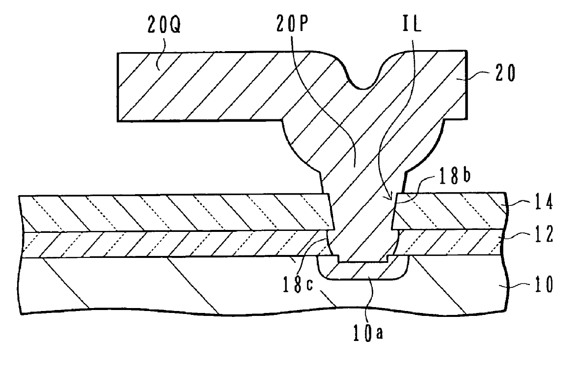
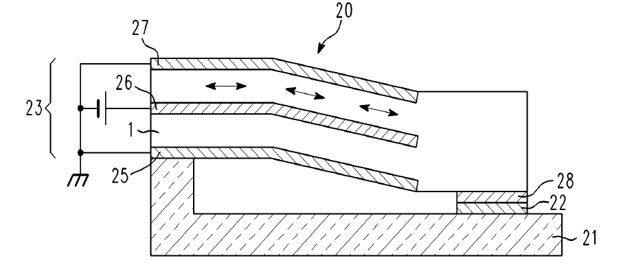
Bimorph and unimorph actuators B81B 2201/032 | A bimorph is a cantilever that consists of two active layers. These layers produce a displacement via: Thermal activation (a temperature change causes one layer to expand more than the other). Electrical activation as in a piezoelectric bimorph (electric field(s) cause one layer to extend and the other layer to contract). A piezoelectric unimorph has one active (i.e. piezoelectric) layer and one inactive (i.e. non-piezoelectric) layer. For example in the following figure, in response to application of a voltage to the first movable electrode 25, the second movable electrode 26, and the third movable electrode 27, the piezoelectric thin film 1 extends/contracts and the movable section 23 is driven toward the substrate 21. |
This place covers:
Processes for manufacturing microstructures on or in a substrate. These processes correspond to two main processing technologies:
- Surface micromachining: techniques for making structures on a substrate by structuring layers of material added on the surface of a support substrate
- Bulk micromachining: techniques for structuring the bulk substrate
This place does not cover:
Assembling of devices or systems from individually processed components |
This place covers:
Processes and arrangements for manufacturing microstructural devices, assembling different parts:
- Bonding parts without damaging further elements (e.g. due to high temperature)
- Aligning elements which have to be assembled
This place covers:
Processes for manufacturing microstructural devices which are not covered by the scope of the groups B81C 1/00 and B81C 3/00 (residual group).
In particular:
- Apparatus for manufacturing microstructural devices
- Post-processing of the microstructural devices
- Manufacturing logistics
- Processes for manufacturing substrate-free devices