CPC Definition - Subclass H01S
This place covers:
Devices using stimulated emission, for the generation or amplification of coherent electromagnetic waves or other forms of wave energy, e.g. masers, lasers, X-ray lasers, gamma lasers, optical amplifiers.
Constructional details or arrangements, e.g. housings, packages, cooling, electrodes.
Configuration of the resonators, or shape of the active media.
Processes or apparatus for pumping (exciting) said devices.
Such functions as modulating, demodulating, frequency-changing, controlling, or stabilising of said coherent electromagnetic waves, insofar these functions are performed by elements being part of the optical resonators or amplifier's arrangements; this includes particularly:
- Frequency multiplying, e.g. harmonic generation
- Pulse-techniques, e.g. Q-switching, mode-locking, or gain-switching.
The special choice or adaptation of materials as active media.
Devices using non-linear amplification effects, e.g. stimulated Raman or Brillouin scattering
This subclass covers functions as modulating, demodulating, frequency-changing, controlling, or stabilising of coherent electromagnetic waves, insofar these functions are performed by elements being part of the optical resonators or amplifier's arrangements, e.g. inside-cavity harmonic generation. Said functions when performed outside the resonators or amplifier's arrangement, e.g. harmonic generation, are covered by subclass G02F.
With regard to the housing or package of a laser or maser, distinction is done between first and second level housing/packages.
A first level housing is considered to be the housing of the laser/maser directly enclosing the (cooled) device. An example for a first level housing is a semiconductor laser or a microlaser in a TO-can (H01S 5/022 and H01S 3/025).
A second level package or housing is considered to be a housing where this TO-can, for example, is integrated like a DVD recorder or a lamp or a beamer.
Second level packages are generally not covered by this subclass but should be in a subclass relating to the application of the device.
Examples of places where the subject matter of this place is covered when specially adapted, used for a particular purpose, or incorporated in a larger system:
Eye surgery using laser | |
Radiation therapy using laser light | |
Sintering by using laser light | |
Working by laser beam, e.g. welding, cutting or, boring | |
Joining of preformed parts by using laser light | |
Laser printers | |
Ring laser gyrometers; fibre laser gyrometers | |
Investigating or analysing colour or spectral properties of materials by using tunable lasers | |
Apparatus specially adapted for photomechanical, e.g. photolithographic, production of textured or patterned surfaces | |
Laser heads for recording or reproducing | |
Laser recording associated with non-optical reproducing, or laser reproducing associated with non-optical recording | |
Trimming by laser in the manufacture of resistors | |
Transmission systems employing light, e.g. all-optical repeaters | |
Photolithographic processing on semiconductor bodies |
Attention is drawn to the following places, which may be of interest for search:
Lamps | |
Measurements using light | |
Measurement of light | |
Optical spectroscopy | |
LIDAR | |
Coupling light guides with opto-electronic elements | |
Laser speckle optics | |
Control of light beams in general | |
Non-linear optics per se | |
Photolithography | |
Scanning | |
Reproduction | |
Displays | |
X-ray generation | |
Plasma generation | |
Semiconductor devices specially adapted for light emission |
In H01S a document is classified according to the features disclosed, i.e. a similar strategy is applied as used for the F-terms of the Japanese patent documentation. Such features can be found, for example, in the figures depicting the embodiments and in the corresponding discussion of these figures in the description. Classification in H01S is not restricted to the wording of the claims or the summary of the invention. Even a detailed prior art device discussed into detail in the disclosure may be classified correspondingly.
In H01S it should be carefully distinguished between defining (e.g. H01S 3/08 or H01S 5/10), controlling (e.g. H01S 3/10 or H01S 5/06-H01S 5/065) and stabilising (e.g. H01S 3/13 or H01S 5/068). This is illustrated with the following example: A grating as one end mirror of the cavity of a laser defines and therefore fixes the wavelength of the laser. As long as it is not disclosed that this grating is intentionally rotated, such a grating will be classified as being a part of the resonator only, e.g. in H01S 3/08009 or in H01S 5/141. As soon as it is disclosed, that the grating is rotated to tune the wavelength, this is considered to fall under a wavelength control by a grating which is classified in H01S 3/1055, for example. When finally a feed-back loop is disclosed, e.g. with the help of a wavelength sensitive detector the intensity at a given wavelength is monitored and kept stable with the help of the feed-back loop, then a group in H01S 3/139 will be allocated. As however in the H01S 3/139 and sub-groups the nature of the wavelength defining reflector is not included, further classes in H01S 3/08 and sub-groups should be used to characterize the resonator details, e.g. the reflector being a grating and the number of resonator mirrors present.
This subclass does not cover light emitting devices where it is merely stated that they are a laser or maser, i.e. where the laser or maser is simply a "black box" without any specific details on the electromagnetic wave generation or feedback on it.
In this place, the following terms or expressions are used with the meaning indicated:
active medium | A medium providing for optical gain by the stimulated emission effect when excited by an excitation (pump) energy source. |
laser | It is the acronym for "light amplification by stimulated emission of radiation" but it also refers, in broader sense, to any device using stimulated emission of radiation by excited atoms.Hence, for example, the expressions "semiconductor laser", "dye laser", "optical fibre laser" or "X-ray laser". |
pumping | The process of providing the active medium for excitation energy. |
In patent documents, the following words/expressions are often used as synonyms:
- active medium: gain medium, lasing medium excitation: pump(ing)
In patent documents, the word/expression in the first column is often used instead of the word/expression in the second column, which is used in the classification scheme of this place:
LASER | Light Amplification by Stimulated Emission of Radiation |
MASER | Microwave Amplification By Stimulated Emission Of Radiation also known as Microwave Laser |
EDFA | Erbium Doped Fibre Amplifier |
SOA | Semiconductor Optical Amplifier |
DBR Laser | Distributed Bragg Reflector Laser |
DFB Laser | Distributed Feed-Back Laser |
This place covers:
Masers, i.e. devices generating or amplifying light by stimulated emission from the infrared to the far-infrared/THz part of the electromagnetic wave spectrum, i.e. wavelengths longer than about 10 microns, e.g. CO2 laser.
Attention is drawn to the following places, which may be of interest for search:
Far-infrared and THz-lasers based on semiconductor lasers | |
Quantum cascade lasers with for example intra-band transitions | |
THz sources where stimulated emission is not explicitly involved, e.g. a fs-laser pulse illuminates an Auston switch or a Josephson contact and THz emission results from accelerating electrons according to the local amplitude of the applied electromagnetic field | |
Inorganic light-emitting semiconductor devices having potential barriers |
This place covers:
Devices generating or amplifying light by stimulated emission from the infrared to the ultraviolet part of the spectrum.
Laser media including gaseous, liquid and solid gain media as a matrix and comprising generally atoms, ions or molecules as dopants having discrete spectral absorption and emission lines or bands.
This place does not cover:
Semiconductor lasers |
Attention is drawn to the following places, which may be of interest for search:
Optical components for lasers per se are classified in the following groups/subclasses:
This place does not cover:
Housings or packages of fibre lasers |
Attention is drawn to the following places, which may be of interest for search:
Gas discharge tubes in general |
This place does not cover:
Reflectors having variable properties or position for initial adjustment of the resonator |
This place does not cover:
Metal vapour lasers |
Attention is drawn to the following places, which may be of interest for search:
Cooling arrangements for gas lasers | |
Gas dynamic lasers | |
Means for obtaining or maintaining the desired gas pressure within the tube in general |
This place covers:
Stepwise change of a dimension or a doping profile, e.g. undoped end caps on a doped laser rod or end flanges having a larger diameter than the part in between
This place does not cover:
Construction or shape of active medium consisting of a plurality of parts |
This place covers:
Devices having a dopant gradient or a changing dimension of the laser crystal, i.e. there must a gradual change in the dopant profile or at least one of the laser material dimensions (e.g. tapering)
Attention is drawn to the following places, which may be of interest for search:
Optical pumping thereof | |
Controlling the output parameters | |
Stabilisation of the output parameters | |
Scattering effects, i.e. stimulated Brillouin or Raman effects | |
Optical fibres and packages comprising optical fibres | |
Transmission using light |
Fibre lasers are not classified in H01S 3/0602-H01S 3/0627
As soon as details specific to amplification by stimulated emission are disclosed, a corresponding group in H01S 3/00 should be given, e.g. details on the amplification bandwidth, control or stabilisation of the fibre amplifier. The fact that for example merely a fibre amplifier is comprised by a device should not result in the allocation of a group in H01S 3/00.
This place does not cover:
Constructional details of the fibre |
Fibre amplifiers are generally not double classified by allocating in addition H01S 3/2308, only in the case of for example double passes etc. a respective coding in H01S 3/2325 and sub-groups is given.
Cascaded fibre amplifiers are only classified in H01S 3/06758 and not in H01S 3/2316.
This place does not cover:
Fibre lasers |
Attention is drawn to the following places, which may be of interest for search:
Waveguide lasers | |
Controlling the laser output | |
Stabilising |
This place does not cover:
Mode suppression using a plurality of resonators |
This place covers:
Laser generates having more than one laser wavelength, e.g. by internal frequency conversion
Outcoupling mirrors being at least partly transmissive for the at least two wavelengths, i.e. at least two laser beams at different wavelengths must be intentionally out-coupled
This place covers:
Devices with multiple bounces off of lateral, non-end mirror surfaces
This place does not cover:
"Active mirror" lasers with a singly folded path through the laser medium, |
Attention is drawn to the following places, which may be of interest for search:
Folded-path gas lasers |
Attention is drawn to the following places, which may be of interest for search:
Longitudinal mode control, e.g. specifically multimode |
This place does not cover:
Fibre ring lasers |
Attention is drawn to the following places, which may be of interest for search:
Ring laser gyrometers |
This place covers:
Pulsed or modulated coherent pumping and no explicit effect of the pumping itself on a pulse forming, e.g. frequently Q-switched lasers are pumped in a pulsed way but the pulse duration is determined by the Q-switch and/or the resonator length and not the pumping means
This place does not cover:
Pulse generation |
This place does not cover:
Details of laser diodes |
Attention is drawn to the following places, which may be of interest for search:
Generating plasma, e.g. by combustion |
This place does not cover:
Free-electron laser | |
Electrical, electrochemical, or electron-beam pumping of a dye laser | |
Gas discharge using an electron or ion beam |
This place does not cover:
Gas discharge using inductive or capacitive excitation |
This place does not cover:
Auxiliary ionisation means for transversely excited lasers, e.g. double discharge excitation |
Attention is drawn to the following places, which may be of interest for search:
Controlling of light beams, frequency-changing, non-linear optics, optical logic elements, in general |
Group H01S 3/10007 takes precedence over groups H01S 3/102 - H01S 3/104
This place covers:
Control as defined in the subclass H01S, i.e. the pulse repetition rate is controlled and not merely defined or fixed
This place does not cover:
Pulse generation, e.g. Q-switching, mode locking |
Attention is drawn to the following places, which may be of interest for search:
Optical-mechanical scanning systems in general | |
Electro-, magneto- or acousto-optical deflection | |
Control of position or direction of light beam generating device in general |
This place does not cover:
Stabilisation of laser output parameters, e.g. frequency, amplitude |
This place covers:
the control of the pulse duration by the intensity or the duration of the coherent or non-coherent pulsed pump source, i.e. the duration of the generated pulse is changed with pump intensity/duration,
Attention is drawn to the following places, which may be of interest for search:
Details of laser diodes e.g. housing, cooling, electric circuitry |
This place does not cover:
Mode locking using a non-linear element |
This place covers:
Q-switching per se without any details of the kind of Q-switching
This place covers:
Devices with dopants in a bulk semiconductor matrix with discrete absorption / emission lines
This place covers:
Ceramic lasers
The solid laser material is additionally classified in H01S 3/163 and the doping in H01S 3/1601.
In the case a laser material is characterized by the (measured and depicted) amplification, H01S 3/2308 should be allocated besides the laser material and doping if appropriate.
Attention is drawn to the following places, which may be of interest for search:
Glass manufacture, shaping or supplementary processes | |
Compositions for laserable glass |
This place covers:
All devices generating or amplifying light by stimulated emission in spectral ranges with wavelengths longer than far-infrared/THz and shorter than ultraviolet.
Attention is drawn to the following places, which may be of interest for search:
X-ray sources where for example a plasma is initiated by a focused femtosecond laser pulse which results in the generation of X-rays |
This place covers:
Semiconductor lasers which are characterized by having a valence and a conduction band with a band-gap in between and light emission due to a transition across at least part of a band-gap or within a band in the case of quantum cascade lasers. In order to tune the laser transition, the composition of the semiconductor and its doping can be designed.
One exception to this rule relates to "organic laser diodes". These devices have generally a layer structure similar to a laser diode comprising a semiconductor substrate and laminate, but the active region comprises an organic material.
Because it is frequently not disclosed whether the transition responsible for light emission is across a bandgap or in between discrete energy states, all such devices are classified in H01S 5/36 because the involvement of the semiconductor layers and the resonator structure being similar to that of a laser diode.
Semiconductor laser can be integrated with other electrical or optical components and has electrical circuitry for driving the laser diode. Details of such components per se are classified in for example the following main groups:
Optical components like lenses, mirrors, gratings | |
Optical fibres, packaging of semiconductor light sources and fibres | |
Beam manipulation and combination | |
Growth of semiconductors | |
Cooling of semiconductors | |
Assemblies of semiconductors | |
Photodiodes | |
Light emitting diodes (LED) | |
Organic light emitting devices (OLED) | |
Electrical circuits | |
Displays |
This place does not cover:
Semiconductor devices with at least one potential-jump barrier or surface barrier specially adapted for light emission |
Attention is drawn to the following places, which may be of interest for search:
Details of external cavity components; Control or stabilisation acting on laser components | |
Construction or shape of optical resonators or components thereof | |
Optical pumping by coherent light of a laser diode | |
Controlling the intensity, frequency, phase, polarisation or direction of the emitted radiation | |
Stabilisation of laser output parameters |
This place covers:
- Optical arrangements that are specific for illuminating fluorescent or phosphorescent materials with radiation emitted from laser diodes.
- Specific arrangements of optical components that are used to guide laser diode beams onto fluorescent or phosphorescent materials like mirrors, lenses or waveguides or specific laser diode arrangements used to illuminate a fluorescent or phosphorescent material. Alternatively, the fluorescent or phosphorescent material may be part of the window of a laser diode package.
This subgroup does not cover specific compositions of phosphors or fluorescent materials. Neither does it cover specific applications of such a light source, like vehicle lamps comprising a laser diode as a black box, without any specific details on how the laser diode emission illuminates the fluorescent or phosphorescent material.
Multi-aspect classification of documents in different sub-classes is considered appropriate in case they disclose, for example, specific details of the laser diode arrangements to illuminate phosphors, a specific manufacturing of phosphors, as well as specific vehicle lamps comprising such light sources in the respective places of classification.
Examples of subject matter to be classified in H01S 5/0087:
- Optical arrangements that are specific for illuminating fluorescent or phosphorescent materials with radiation emitted from laser diodes.
- Specific arrangements of optical components.
Examples of places where the subject matter of this place is covered when specially adapted, used for a particular purpose, or incorporated in a larger system:
Light sources using semiconductor devices, as light- generating elements, using wavelength conversion distinct from the light-generating elements | |
Lighting devices or systems specially adapted for vehicles with specific type of light source for headlamps |
Attention is drawn to the following places, which may be of interest for search:
Luminescent materials containing rare earth elements | |
Lighting devices or systems specially adapted for vehicles with specific type of light source for headlamps with phosphor and source being spaced apart | |
Light filters with selection of luminescent materials for screens for lightning devices, e.g. luminaires or lightning modules | |
Light generating elements of semiconductor light sources being semiconductor laser screens for lightning devices, e.g. luminaires or lightning modules | |
Projectors or projections type viewers with lamp houses characterized by using LED or laser light sources and secondary light emission |
Attention is drawn to the following places, which may be of interest for search:
Nonlinear frequency conversion per se |
This place covers:
First level packages, e.g. a laser diode in a TO can or a butterfly housing.
Attention is drawn to the following places, which may be of interest for search:
Packaging and electrical lead-through per se |
This place covers:
Specific optical components in the laser beamline with the optical components being located inside the laser diode housing or forming part of the housing, e.g. the laser diode emission leaves the housing along a specific optical component.
Attention is drawn to the following places, which may be of interest for search:
Optical components external to the laser cavity, specially adapted therefor, e.g. for homogenisation or merging of the beams or for manipulating laser pulses, e.g. pulse shaping | |
Mountings or housings characterised by the shape of the housings |
This place covers:
Out-coupling of light using lenses that are in the laser beamline and are located inside the laser diode housing or form part of the housing.
The way of classifying optical components inside a laser diode housing is explained with the help of the following example as depicted in the figure below:
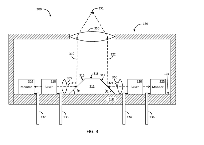
The lens 350 is an optical component in the laser beamline and forming part of the housing 130 and is classified in group H01S 5/02253.
The beam steering mirrors 316,317 following the laser diodes 310 are classified in group H01S 5/02255.
This place covers:
Out-coupling of light using beam deflecting elements that are in the laser beamline and are located inside the housing or form part of the housing.
This place covers:
Out-coupling of light using windows that are in the laser beamline and form part of the housing.
The relationship with other classification places is explained with the help of the following example as depicted in the figure below:
The phosphor forming part of the window is classified in group H01S 5/0087.
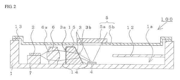
The window 110 comprises a phosphor 111 and is part of the laser diode housing 100 and is classified in group H01S 5/02257.
The beam steering mirrors 40 following the laser diodes 20 are classified in group H01S 5/02255.
The specific lenses 90 in the beamline inside the housing are classified in group H01S 5/02253.
This place covers:
Stems being a portion of a package that is offset or at an angle to the remainder in order to mount the laser diode.
Stems made from a specific material or having specific dimensions or shape. Stems are frequently part of the mounting of laser diodes in a TO-CAN package. This symbol is not allocated for the mere presence of a stem where the packaged laser diode is mounted on and the stem having a shape without any specific function.
Stems made from a material so that it takes the function of a heat spreader should also be classified for that aspect in group H01S 5/02476.
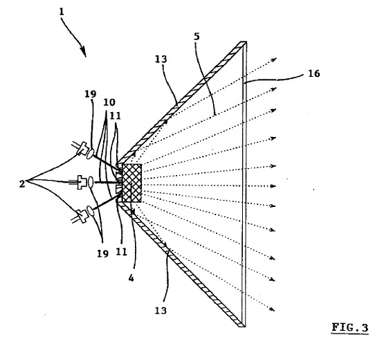
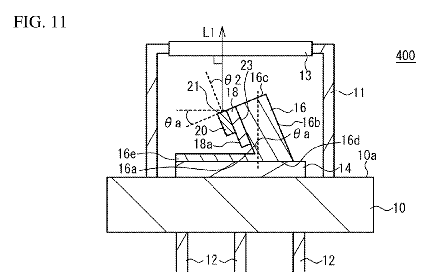
An example of a stem which should be classified in this group is stem 16 having a very specific shape.
Attention is drawn to the following places, which may be of interest for search:
Can-type, e.g. TO-CAN housings with emission along or parallel to symmetry axis | |
Heat spreaders, i.e. improving heat flow between laser chip and heat dissipating elements |
This place covers:
Support members which carry only a laser diode and which are made from a specific material or having specific dimensions or shape.
Support members made from a material so that it takes the function of a heat spreader should also be classified for that aspect in group H01S 5/02476.
This symbol is not allocated for a support member which carries besides the laser diode further specific optical or electrical elements. Such arrangements are classified in groups H01S 5/02325, H01S 5/02326 and H01S 5/0239 if applicable.
Attention is drawn to the following places, which may be of interest for search:
Heat spreaders, i.e. improving heat flow between laser chip and heat dissipating elements |
This place covers:
Laser diodes which are mounted directly or via sub-mounts on a lead-frame.
A lead-frame is a thin sheet of metal with a central pad and outer leads to facilitate electrical connection between a device on the central pad and other devices.
A non-exclusive list of exemplary lead-frame packages include quad flat no-leads packages (QFN), quad flat packages (QFP), dual in-line packages (DIP) and dual-flat no-leads (DFN).
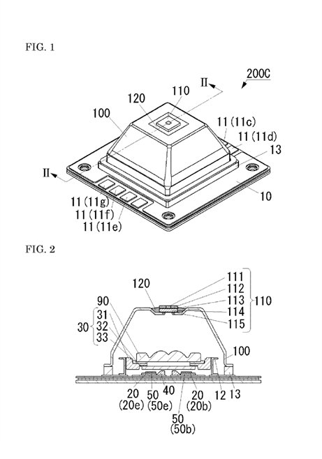
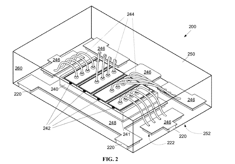
An example for a lead-frame 220 which should be classified in this group is shown below.
Fig. 2 depicts an array of laser diodes mounted on a lead frame with one common electrode on the central pad.
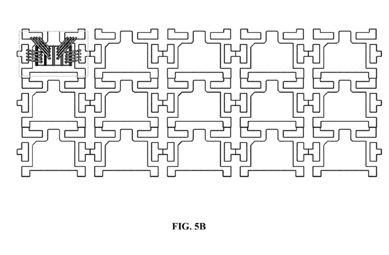
Fig. 5B shows for clarification lead frames without the mounted laser diodes in a stage of manufacturing before singularization into single lead frames.
This place covers:
Positioning of a laser diode on a mount with the help of for example marks on the mounting surface or marks on the semiconductor chip. A mark can also be implemented by correspondingly shaped contact surfaces on the mounting surface of a mount, e.g. self-alignment.
Specific positioning of the laser diode relative to optical components being also mounted on the same mount with the help of for example grooves or stops formed in the surface of the mount is classified in group H01S 5/02326.
Attention is drawn to the following places, which may be of interest for search:
Support members, e.g. bases or carriers |
This place covers:
Combinations of electrical elements and/or combinations of optical elements on the same mount or in the same housing as the laser diode. Such combinations should only be classified in this place if the mount or the housing are specially adapted for the combinations or if a particular layout is provided.
Attention is drawn to the following places, which may be of interest for search:
Non-optical elements | |
Cooling solid state junction devices |
This place does not cover:
Stabilisation of output |
Attention is drawn to the following places, which may be of interest for search:
Coupling light guides with opto-electronic elements | |
Devices consisting of a plurality of semiconductor or other solid state components formed in or on a common substrate, adapted for light emission |
This place covers:
- Electrodes of a semiconductor laser with at least one electrode having a specific shape.
- Electrodes having a geometrical shape like a square, triangular or a circular shape for specific reasons given in the document.
- Electrodes having defined dimensions, e.g. a specific electrode diameter is disclosed.
Additional symbols may be allocated if appropriate for further specific aspects of electrodes from the following places H01S 5/04252, H01S 5/04253, H01S 5/04256 and H01S 5/04257.
This place covers:
- Electrodes of a semiconductor laser with at least one electrode having a specific configuration, e.g. the placement of the electrode within an electric circuit.
- Electrodes having specific geometric arrangement, e.g. electrodes with specific distances or specific geometric arrangements between/among them, e.g. an array of VCSEL with the electrodes arranged in the shape of a honeycomb or concentric circles.
Additional symbols may be allocated if appropriate for further specific aspects of electrodes from the following places H01S 5/04252, H01S 5/04253, H01S 5/04254 and H01S 5/04257.
This place covers:
Control/stabilisation by applying voltages to the electrodes of the semiconductor laser chip or temperature tuning of the laser diode itself;
Attention is drawn to the following places, which may be of interest for search:
Control/stabilisation of the external cavity elements | |
Transmission systems employing light |
This place covers:
Frequency conversion inside the semiconductor laser chip
This place does not cover:
SHG in an external cavity is |
This place does not cover:
Mode locking; Mode suppression; Mode selection; Self pulsating |
This place does not cover:
Multi-section lasers |
This place covers:
Circuitry comprising diodes for overvoltage or surge protection
Attention is drawn to the following places, which may be of interest for search:
Monolithic integration |
This place does not cover:
Structure or shape of the semi-conductor body to guide the optical wave; Confining structures perpendicular to the optical axis, e.g. index- or gain-guiding, stripe geometry, broad area lasers, gain tailoring, transverse or lateral reflectors, special cladding structures, MQW barrier reflection layers |
This place covers:
Structures of the laser diode chip (and its waveguide)
This place does not cover:
Laser diode with an external ring resonator for wavelength definition |
This place does not cover:
Attention is drawn to the following places, which may be of interest for search:
Forward coupled structures, i.e. DFC lasers |
This place does not cover:
Mode locking; Mode suppression; Mode selection | |
Surface-emitting [SE] lasers |
Attention is drawn to the following places, which may be of interest for search:
For external cavity lasers covered by H01S 5/14 the group H01S 5/06 is additionally allocated for the control/stabilisation by applying voltages to the electrodes of the semiconductor laser chip or temperature tuning of the laser diode itself.
In this group external cavity elements correspond to elements inside the laser cavity or forming part of the cavity but outside of the semiconductor laser chip. Specific optical elements forming part of the external cavity and their control should also be classified in H01S 3/08, H01S 3/10 and H01S 3/13.
As an example, Fig. 8 is discussed.
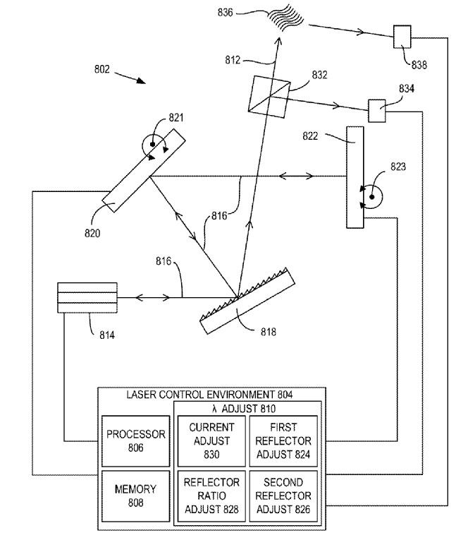
H01S 5/143: The ECLD is in a Littman-Metcalf configuration, this is the basic configuration of the laser.
Details of the external cavity elements are classified in H01S 3/00:
H01S 3/105: The tilt of one mirror is used for wavelength control;
H01S 3/139: The tilt of one mirror is controlled with a feed-back loop for stabilisation of the set wavelength; and H01S 3/0816: The resonator has 4 reflectors counting also the reflecting back facet of the laser diode chip.
This place covers:
Surface emitting lasers having only a vertical cavity.
In case of so called "half VCSEL" which are used as a gain medium in for example external cavity laser diodes or in case the VCSEL is coupled to resonator elements integrated into a photonic circuit still the details of the VCSEL chip itself are classified in group H01S 5/183 independent of the geometrical arrangement of the external cavity.
Attention is drawn to the following places, which may be of interest for search:
Comprising a photonic bandgap structure |
This place covers:
Surface emitting lasers having only a horizontal cavity. The surface emission may be realized by a beam deflecting mirror external to the semiconductor laser chip but manufactured into the semiconductor layer structure by for example etching. I.e., the beam deflecting element is an integral part of the semiconductor laser structure.
Surface emission resulting from an edge-emitting semiconductor laser and a separate beam deflecting element both being arranged on a mount is classified in group H01S 5/02255.
In case the output coupling is performed with the help of a photonic bandgap structure in addition classification in group H01S 5/11 should be considered.
This place does not cover:
Construction or shape of the optical resonator comprising a photonic bandgap structure |
Attention is drawn to the following places, which may be of interest for search:
Support members, e.g. bases or carriers |
Attention is drawn to the following places, which may be of interest for search:
Surface-emitting [SE] lasers having only vertical cavities, e.g. vertical cavity surface-emitting lasers [VCSEL] |
This place covers:
Specific layers of the laser diode chip or materials provided therein or structures manufactured into the semiconductor body that have an impact on the wave-guiding properties of the laser diode. Both alternatives are covered here: index guiding or anti-guiding as well as gain guiding. See the corresponding entries for the correct classification of a document.
The range H01S 5/2004 - H01S 5/205 restricts itself to structures having a wave-guiding effect in a direction being perpendicular to the layer structure, which equals in most cases a wave-guiding impact along the growth direction.
Gain guiding in the perpendicular direction by shaping the active region by a thickness variation along the optical axis is in H01S 5/106.
Wave-guiding in a direction being parallel to the layer structure can be found in for example:
- H01S 5/1003 - H01S 5/1017 (index guiding)
- H01S 5/1064 (gain guiding)
This place covers:
Structures or layers having a wave-guiding effect in a direction being perpendicular to the layer structure, which equals in most cases a wave-guiding impact along the growth direction. Often used for selecting or suppressing optical modes inside the laser diode chip.
The range H01S 5/2004 - H01S 5/205 restricts itself to structures having a wave-guiding effect in a direction being perpendicular to the layer structure, which equals in most cases a wave-guiding impact along the growth direction. Gain guiding in the perpendicular direction by shaping the active region by a thickness variation along the optical axis is in H01S 5/106.
This place covers:
Electron barrier layers that are used to confine the electrical charges into a certain zone comprising the active region. This confinement results in a confined gain region, which in turn is responsible for an impact of gain guiding on the modes propagating inside the laser diode chip. Electron barrier layers manifest themselves frequently by being a highly doped and thin semiconductor layer with a thickness in the few nanometer range.
Gain guiding in the perpendicular direction by shaping the active region by a thickness variation along the optical axis is in H01S 5/106.
This place does not cover:
Buried mesa structure; Striped active layer |
This place covers:
Asymmetric protrusions comprised in the layer structure, i.e. only one step in the height of the substrate or the laminate,
This place does not cover:
The active region comprising quantum well, quantum wire, quantum box or supperlattice structures, e.g. single quantum well lasers (SQW lasers), multiple quantum well lasers (MQW lasers), graded index separate confinement hetrostructure lasers (GRINSCH lasers) | |
The active region comprising organic materials |
This place covers:
Doping with small amounts of group III or V compounds
This place does not cover:
The active region comprising organic materials |
Attention is drawn to the following places, which may be of interest for search:
Doping with small amounts of group III or V compounds |
Attention is drawn to the following places, which may be of interest for search:
Dye lasers |
This place does not cover:
Structural details or components not essential to laser action | |
Processes or apparatus for excitation | |
Arrangements for controlling the laser output parameters | |
Construction or shape of the optical resonator | |
Structure or shape of the semi-conductor body to guide the optical wave; Confining structures perpendicular to the optical axis | |
Structure or shape of the active region; Materials used for the active region | |
Amplifier structures not provided for in groups H01S 5/02 - H01S 5/30 |
This place covers:
Master oscillator and (power) amplifier arrangements (MOPA), i.e. the wavelength of the amplifier is the same as of the laser diode acting as the oscillator
This place covers:
Laser diode arrays / bars
This place does not cover:
Cooling of laser diode bars | |
Arrays of surface emitting lasers |
External cavity lasers are additionally classified in group H01S 5/06 and sub-groups when the control/stabilisation by applying voltages to the electrodes of the semiconductor laser chip or temperature tuning of the laser diode itself is of interest.
This place covers:
Arrays of surface emitting lasers as classified in groups H01S 5/18, H01S 5/185 and H01S 5/187.
In order to be able to distinguish between arrays of horizontal or folded cavity surface emitting lasers classification in group H01S 5/42 should always be accompanied by the additional classification in appropriate groups H01S 5/18, H01S 5/185 or H01S 5/187.
This place covers:
Arrays of vertical cavity surface emitting lasers as classified in group H01S 5/183.
Attention is drawn to the following places, which may be of interest for search:
Measuring arrangements for measuring contours or curvatures | |
Systems according to group G01S 17/00 using multiple transmitters | |
3D imaging with simultaneous measurement of time-of-flight at a 2D array of receiver pixels, e.g. time-of-flight cameras or flash lidar |
Attention is drawn to the following places, which may be of interest for search:
Amplifier structures as repeaters in transmission systems |