SECTION I - CLASS DEFINITION
This class provides for active solid-state electronic devices, that
is, electronic devices or components that are made up primarily
of solid materials, usually semiconductors, which
operate by the movement of charge carriers - electrons
or holes - which undergo energy level changes within the
material and can modify an input voltage to achieve rectification, amplification, or switching
action, and are not classified elsewhere.
SCOPE OF THE CLASS
Active solid-state electronic devices include diodes, transistors, thyristors, etc., but
exclude pure resistors, capacitors, inductors, or
combinations solely thereof. The latter class of devices
is characterized as passive.
The subject matter to be found here includes only active solid-state
devices, per se. It may include one or more such
devices combined with contacts or leads, or structures
configured to be tested on a semiconductor chip, or merely
semiconductor material without contacts or leads where the sole
disclosed use is an active solid-state device.
This subject matter does not include
active solid-state devices combined with significant circuits.
Claims reciting an integrated circuit nominally with significant
metallization will be classified in Class 257, whereas
otherwise, nominal recitation of an integrated circuit (i.e., without
significant active solid-state device recitation) will
not be sufficient to permit the device to be classified in Class
257.
KEY CONCEPTS
See Subclass References to the Current Class, below, for references
that relate to key concepts and terms found in Class 257.
An indication that a particular concept or term occurs in one or
more subclasses does not mean that the indicated subclass or subclasses
are the only places that subject matter may be found.
That subject matter may possibly be found elsewhere in Class 257 listed
under a related term or concept that may be broader or narrower
or of the same scope.
OTHER CLASSIFICATION SYSTEMS
Each subclass definition may contain an OTHER CLASSIFICATION
SYSTEMS listing that is to be used for informational purposes only.
These classification listings may change at any time after their
publication and are therefore not guaranteed to be current.
In addition, the classification listing does not necessarily
indicate the sole relationship between the U.S. Patent Classification
System and foreign classifications. Even where a single
classification is listed for a single U.S. subclass, a
one-to-one correlation should not be inferred.
As a result, information contained therein is considered
to be only a guide to related subject matter.
SECTION II - LINES WITH OTHER CLASSES AND WITHIN THIS CLASS
A. Classes related to Class 257 subject matter in
the sense that they employ active solid-state devices in
electronic circuits and the relationship of these classes to Class
257 is mainly that of a combination to a subcombination or of a
genus to a specie. See References to Other Classes, below, referencing
this section.
B. Classes related to Class 257 subject matter in
the sense that they employ active solid-state devices in
electronic circuits and the use of active solid-state electronic devices
primarily as a perfecting feature. See References to Other
Classes, below, referencing this section.
C. See References to Other Classes below for classes that
provide for materials used in active solid-state electronic
devices.
D. See References to Other Classes, below, for
classes related to Class 257 because they provide for methods of
making, cleaning, coating, etc., active
solid-state devices, e.g., Class
438, Semiconductor Device Manufacturing: Process.
E. See References to Other Classes, below, for
Classes related to Class 257 because they provide for active solid-state
electronic devices structures with a specified use, e.g., Class
136, Batteries: Thermoelectric and Photoelectric.
F. See References to Other Classes, below, for
classes providing for provide for subcombination subject matter
that can be used as component part of active solid-state
electronic devices (e.g., lead
frames) or perfect the device (e.g., a
heat sink).
G. Classes which provide for passive solid-state
electronic devices with names that may refer to either active or
passive solid-state electronic devices, e.g., coherers, varistors, varactors. luminescent
or electroluminescent devices. The devices may be part
of the main subject matter of the class or may be used as circuit
elements in circuits or control or measuring systems which form
the main subject matter of the class.
See References to Other Classes, below, referencing
this section.
SECTION III - SUBCLASS REFERENCES TO THE CURRENT CLASS
SEE OR SEARCH THIS CLASS, SUBCLASS:
| 1, | through 8, for bulk effect device. |
| 2, | - 5, 16, 52-63, and
646, for amorphous semiconductor material. |
| 4, | 72, 91, 144, 150, 151, 175-177, 181, 182, 207-211, 246-250, 276, 309, 317, 401, 448, 457, 459, 503, 508, 573, 584, 587, 602, 621, 625, 666-676, and
692-697, for configuration of electrode, contact, lead
or pad. |
| 4, | 32, 33, 81, 91, 99, 144, 150-153, 177-179, 181, 182, 203, 207-211, 276, 377, 382-385, 459, 503, 522, 554, 573, 576, 584, 602, 621, 625, 661-677, 690-700, and
734-786, for electrical contact or lead. |
| 6, | through 8, for Gunn effect (intervalley
transfer). |
| 7, | for intervalley transfer (e.g., Gunn) device
in integrated circuit. |
| 10, | through 11, and 407, for controlled
work function material. |
| 10, | and 11, for electron emissive layer. |
| 10, | through 27, and 104-106, for
heterojunction involving quantum-mechanical tunneling. |
| 10, | and 11, for photocathode. |
| 10, | 54, 73, 155, 192-195, 217, 260, 267, 269, 275-277, 280-284, 449-457, 471-486, and
928, for Schottky barrier. |
| 10, | 11, 30-39, and 314-326, for
tunneling-insulator layer. |
| 10, | 11, and 407, for work function
of material, controlled, e.g., low. |
| 13, | 76, 78, 85, 90, and
94-97, for heterojunction light emitter. |
| 13, | 79-103, and 918, for
light emitting device. |
| 13, | through 25, for quantum well device. |
| 15, | through 22, and 28, for superlattice. |
| 16, | 55, 63, and 65, for heterojunction
in non-single-crystal material. |
| 18, | 19, and 190, for mismatched or
strained lattice. |
| 18, | 19, and 190, for mismatch of lattice
constant. |
| 18, | and 19, for strained layer superlattice
heterojunction. |
| 19, | 76, 78, 103, 200-201, and
613-616, for alloy of two different semiconductors (e.g., GaxIn1-xAs). |
| 20, | 24, 27, 57-61, 66-72,
133-145, 192-195, 202-211, 213, and
252-413, for field effect devices. |
| 20, | 24, and 194, for HEMT (High
electron mobility transistor). |
| 20, | 27, 187, and 192-195, for
heterojunction FETs. |
| 21, | 85, 184-189, for heterojunction
in light responsive device. |
| 21, | for light responsive or activated device (superlattice
quantum well heterojunction). |
| 21, | 53-56, 59, 72, 80-85, 113-118, 184-189, 222, 223, 225-234, 257, 258, 290-294, 325, 428-466, 680, 681, and
749, for radiation responsive. |
| 21, | and 187, for light responsive heterojunction transistor. |
| 21, | 187, 443, and 462, for
photosensitive bipolar transistor. |
| 26, | 27, and 29, for ballistic transport
device. |
| 26, | 27, and 29, for ballistic transport
transistor. |
| 31, | through 36, for Josephson device. |
| 31, | through 36, and 661-663, for
superconductive element/device. |
| 31, | through 36, 468, and 661-663, for
thermal device operated at cryogenic temperature. |
| 33, | for high temperature (30 K) Josephson
device. |
| 40, | for organic semiconductor material. |
| 41, | for point contact device. |
| 42, | for Selenium (elemental). |
| 44, | through 47, for alloyed junction. |
| 45, | for thermal gradient zone melting (TGZM). |
| 46, | 104, and 105, for Esaki diode. |
| 46, | and 104-106, for p-n
junction type (Esaki type) tunneling. |
| 47, | 197, 205, 273, 350, 361, 370, 378, 423, 462, 477
though 479, 511, 512, 517, 518, 525, 526, 539-543, and
552-593, for bipolar transistor structure. |
| 47, | for alloyed junction bipolar transistor. |
| 48, | and 797, for calibration or test structure.5, for array
of bulk effect amorphous switches. |
| 48, | for test structures. |
| 49, | through 75, for non-single crystal, as
active layer. |
| 49, | through 51, 64-75, 359, 377, 380-382, 385, 412, 505, 518, 520, 524-527, 538, 554, 576, 581, 588, and
754-757, for polycrystalline semiconductor material. |
| 49, | through 51, and 64-75, for
polycrystalline active junction material. |
| 49, | through 51, and 64-75, for
recrystallized active semiconductor layer. |
| 50, | and 530, for anti-fuse component
or element. |
| 50, | 530, and 928, for shorted devices, in
general, e.g., anti-fuse
elements. |
| 53, | through 56, for amorphous semiconductor material
device. |
| 53, | through 56, 108, 225, 252, and
414, for responsiveness to nonelectric signal. |
| 55, | and 63, for alloy of
amorphous semiconductor materials. |
| 55, | 63, and 65, and 646,
for silicon nitride to increase band gap of amorphous or polycrystalline
silicon. |
| 56, | 58, 62, and 65, for for
dangling bond. |
| 56, | 58, 62, and 68, for passivation
of dangling bonds in nonsingle crystal semiconductor. |
| 57, | through 61, 66-72, and
368-401, for insulated gate FET in integrated
circuit. |
| 57, | through 61, and 66-72, for
FET in non-single crystal or recrystallized semiconductor
material (e.g., amorphous or
polycrystalline semiconductor as channel). |
| 59, | 72, and 88-93, for array
as imager, or with transparent electrode, or as
display (with plural light emitters). |
| 59, | 72, 449-457, and 749, for
electrical contact or lead transparent to light. |
| 59, | 72, and 293, for photoresistor
combined with accessing FET. |
| 59, | 72, 453, and 749, for
transparent electrode. |
| 60, | 135, 136, 263-267, 302, and
328-334, for vertical channel field effect device. |
| 64, | 255, 521, 627, and 628, for
crystal axis or plane. |
| 65, | for alloy of polycrystalline semiconductor materials. |
| 66, | 67, 69, 379-381, 903, and
904, for static memory cell using FET. |
| 67, | through 70, for stacked FETs. |
| 67, | 69, 70, and 74, for stacked
FETs. |
| 68, | through 71, 296-313, 296, 298, 300, 906, and 908, for
capacitance combined with insulated gate device. (e.g., DRAM). |
| 68, | 71, and 295-313, for
insulated gate device (capacitor or combined with capacitor). |
| 68, | 71, 296-313, and 905-908, for
memory device component involving a capacitor (e.g., dynamic
memory cell). |
| 68, | 71, 303, and 306-309, for
stacked capacitors in DRAM cell. |
| 68, | and 301-305, for capacitor in
trench. |
| 68, | 283, 284, 330-334, 374, 397, 513, 514, 622, 647, and
648, for vertical walled groove in semiconductor. |
| 69, | 195, 204, 206, 338, 350, 351, 357-359, and 365-377, for
CMOS. |
| 69, | 195, 204, 206, 274, 338, 350, 351, 357-359, and
369-377, for complementary field effect transistors. |
| 74, | and 278, for three-dimensional
integrated circuit. |
| 76, | through 78, and 183-201, for
heterojunction, generally. |
| 76, | through 78, for wide band gap semiconductor material
other than GaAsP or GaAlAs. |
| 80, | through 85, for light responsive or activated device
combined with light emitting device. |
| 81, | 99, 177-181, 584, 625, 675, 688, 689, 705, 707, 712-722, and
796, for heat sink. |
| 81, | 82, and 99, for housing or package
for light emitter. |
| 81, | and 82, for housing or package for light
emitter combined with light receiver. |
| 81, | 82, 433, 434, 680, 681, for
housing or package for light responsive device. |
| 81, | 99, and 666-677, for
lead frame. |
| 83, | for light coupled transistor structure. |
| 86, | and 87 for indirect band gap active layer - light emitter. |
| 87, | 131, 156, 439, 523, 590, and
608-612, for deep level dopant/impurity. |
| 87, | 126, 131, 156, 523, 590, 609-612, and
617, for recombination centers. |
| 91, | 98, 151, 175, 176, 249, 250, 276, 282-284, 309, 317, 401, 418, 435, 448, 457, 459, 503, 508, 534, 573, 587, 602, 621, 662, and
664, for shape(d) contact, electrode, conductor, or
terminal. |
| 91, | 98, 294, 323, 435, and
659, for optical shield. |
| 93, | for plural light emitters in integrated circuit. |
| 93, | 374, 446, 499 and 564, for
electrical isolation of components in integrated circuit. |
| 95, | 117, 118, 127, 170, 244, 283, 284, 301-305, 330-334, 418, 419, 447, 460, 466, 496, 534, 571, 586, and
618-628, for grooves, generally. |
| 95, | 170, 171, 452, 466, 496, 571,
586, 594, 600, 618, and 623-626, for
mesa structure. |
| 95, | for shaped contact, electrode, etc., external
of heterojunction light emitter. |
| 98, | 116, 117, 294, and 432, for
light fiber, guide, or pipe. |
| 98, | for luminescent material used with light emitter. |
| 98, | 181, 418, 688, 710, 711, 728, and
730, for shaped housing or package. |
| 98, | 99, 116, 434, 680, and
681, for window (optical) for housing. |
| 100, | 433, 434, 667, 687, 767-and
796, for encapsulated. |
| 101, | 194, 219-221, 264, 269, 285, 335-345, 404, 430, 450, 458, 463, 492, 493, 497, 498, 543, 545, 548, 558, 583, 591, 592, 596, 597, 605, 606, 655-657, 927, and
929, for dopant/impurity concentration, incl., graded
profile. |
| 102, | 227, 439, and 607-612, for
specified, generally (e.g., photoionizable). |
| 106, | for reverse conducting diode (tunnel diode). |
| 106, | for Zener diode. |
| 107, | through 182, and 918, for regenerative
switching device. |
| 108, | 252, and 421-427, for
magnetic field responsive. |
| 108, | 225, 254, and 415 and-419, for
device responsive to pressure. |
| 108, | 222, 225, 254, and 417-419, for
strain sensor. |
| 108, | 225, 252, and 467-470, for
passivating device responsive to temperature. |
| 109, | for Shockley diode. |
| 110, | and 119-131, for bidirectional
device (diac, rectifier). |
| 113, | through 118, for regenerative-type
switching device. |
| 115, | 123, and 157-161, for
amplified gate in thyristor. |
| 121, | for reverse conducting thyristor. |
| 121, | for Static Induction Transistor (SIT) - Bipolar transistor
as reverse path of bidirectional conducting thyristor. |
| 122, | 141, 146, and 162, for
lateral structure in regenerative device. |
| 124, | 125, and 133-145, for
FET in or combined with thyristor. |
| 125, | 137, 138, 143, and 149, for
shunt, regenerative device. |
| 125, | 137, 138, 143, 149, and
154, for shorted emitter, anode or cathode, in
thyristor. |
| 127, | 446, 510-522, 571, 577, and
594, for groove to define plural devices. |
| 127, | 170, 339, 372-376, 394-400, 409, 452, 484, 490, 493-495, and
605, for guard ring or region. |
| 131, | 156, 376, 424, 523, 590, and
617, for crystal damage. |
| 133, | 145, 195, 205, 273, 337, 350, 361, 362, 370, and
378, for field effect combined with bipolar type (including
regenerative type) device. |
| 134, | through 136, 217, 256-287, and
504, for JFET. |
| 136, | 205, 264, 268, 269, 392, for
enhancement mode. |
| 139, | through 145, and 212, for conductivity
modulated transistor. |
| 139, | through 145, 147-153, for
extended latching current device. |
| 139, | through 145, 147-153, and
372-376, for means to prevent latchup. |
| 139, | through 145, and 211, for conductivity
modulated transistor. |
| 142, | 148, 376, 553, and 583, for
doping for gain reduction. |
| 146, | 476-479, and 499-564, for
structure with elec. isolated components. |
| 150, | 151, 177-181, for housing
or package for regenerative type switching device. |
| 154, | 169, 194, 195, 218, 264, 523, 646, and
656, for high resistivity semiconductor region - see, also,
intrinsic material; PIN device. |
| 154, | 350, 358, 359, 363, 379-381, 516, 533, 536-543, 571, 572, 577, 580-582,
and 904, for resistive element (resistor) (passive
device). |
| 164, | and 580-582, for ballasting of
current (e.g., by resistors). |
| 164, | through 166, 560-561, 563, and
579- 581, for multiple/plural emitter. |
| 170, | for edge, beveled - preventing
breakdown. |
| 171, | 496, 586, and 618+, for
bevel. |
| 171, | 452, 483, and 484, for
protection against edge breakdown. |
| 171, | and 496, for reverse bevels. |
| 173, | 174, 328, 355-363, 487-496, and
546, for protection against overcurrent or overvoltage. |
| 173, | 529, 665, and 910, for
fuse/fusible link. |
| 173, | for overvoltage protection means in thyristor. |
| 177, | through 181, 467, 468, 573, 625, 675, 688, 705-707, and
712-722, for cooling. |
| 178, | 179, and 746-748, for
stress avoidance between electrode and semiconductor. |
| 178, | through 179, 633, 747, and
748, for thermal expansion matching or compensation. |
| 180, | and 733, for stud-type mount for
housing. |
| 180, | and 733, for stud mount. |
| 181, | 182, 688, 689, 726, 727, and
785 for press contact of electrode and semiconductor. |
| 183.1,
193, | 215-251, and 912, for
charge transfer device. |
| 184, | through 189, for heterojunction. |
| 185, | and 191, for graded band gap. |
| 185, | for staircase (light responsive heterojunction). |
| 187, | 197, and 198, for heterojunction
bipolar transistor. |
| 198, | for wide band gap emitter heterojunction bipolar
transistor. |
| 199, | 481, 482, 551, and 603-606, for
avalanche diode. |
| 199, | 482, and 604, for IMPATT. |
| 199, | 259, 275-277, 482, 523, 604, 624, 625, 659, 662, 664, and
728, for for microwave device component. |
| 202+, | and 909, for master slice (gate
array). |
| 202+, | and 909, for gate arrays. |
| 202, | through 211, and 909, for gate
arrays. |
| 205, | 273, 350, 361, 370, and
378, for bipolar combined with field effect type device. |
| 205, | 273, 350, 361, 370, and
378, for bipolar transistor structure combined with FET. |
| 206, | 208, 210, and 211, for
configuration of elements in gate array. |
| 209, | for gate array with programmable signal paths. |
| 210, | and 758-760, for multi-level
metallization. |
| 212, | for double-base diode (unijunction
transistor). |
| 212, | for Static Induction Transistor (SIT) - Unijunction
transistor. |
| 212, | for unijunction transistor. |
| 214, | for charge injection device. |
| 215, | 218, and 225-251, for
surface channel charge transfer device. |
| 216+, | for bulk channel device. |
| 216, | and 285, for buried channel. |
| 219, | through 221, for nonuniform channel doping
in buried channel CCD. |
| 223, | 230, and 445, for antiblooming. |
| 223, | 230, and 445, for suppression
of blooming in light imager. |
| 224, | and 243, for channel confinement. |
| 225, | 253, and 414, for chemical sensor. |
| 225, | for CCD with fixed pattern memory as ROM. |
| 228, | 447, 460, for backside illumination. |
| 239, | for floating diffusion as CCD Output Tap. |
| 239, | 261, and 315-323, for
floating gate. |
| 240, | for nonuniform channel thickness in CCD. |
| 241, | for parallel channels in CCD. |
| 245, | 364, and 489, for resistive electrode. |
| 246, | through 248, for nonuniform channel doping
in CCD, for directionality. |
| 249, | 317, 359, 363, 364, 377, 380-382,
384, 385, 387, 407, 412, 413, 489, 505, 518, 520, 524-527, 538, 554, 576, 581, 588, 646, 754-756, 904, and
914, for polycrystalline material (including polysilicon
contacts) other than active junction material. |
| 251, | for bucket-brigade device. |
| 254, | and 416, for acoustic
energy detector. |
| 256, | and 257, for light responsive PIN device
combined with JFET. |
| 257, | and 258, for JFET. |
| 227, | and 439, for photoionization. |
| 258, | 291-294, 443-448, and
911, for array of electrode field effect devices. |
| 260, | and 262, in or combined with a JFET device. |
| 260, | and 261, for memory device component involving
a JFET (e.g., taper isolated
or floating pn junction gate type). |
| 265, | for vertical current path JFET in integrated circuit. |
| 266, | 267, and 287, for parallel channels
in JFET. |
| 269, | and 285, for nonuniform channel doping
in JFET. |
| 272, | through 278, for JFET in integrated circuit. |
| 275, | through 278, 662, and 664, for
stripline lead. |
| 276, | for air bridge electrical lead. |
| 276, | for air bridge contact. |
| 283, | and 284, for groove alignment of Schottky
gate to source region in MESFET. |
| 283, | through 284, 330-334, for
gate electrode of FET formed in groove. |
| 286, | for nonuniform channel thickness in JFET. |
| 290, | and 294, for IGFET. |
| 291, | through 294, 326, 334, 337, 338, 347-363, and 368-401, for
insulated gate device (IGFET in integrated circuit). |
| 294, | 297, 340, 409, 435, 488-490, 503, 508, 630, 659-660, and
662, for shield electrode. |
| 295, | 298, and 314-326, for
EPROM/EEPROM. |
| 295, | 298, 314, and 324-326, for
MNOS insulated gate-type memory device component. |
| 297, | 349, 547, and 620, for
means to prevent charge leakage or leakage current. |
| 297, | 349, 354, 372-376, 503, 547, and
620, for means to prevent leakage current or charge leakage. |
| 297, | 660, and 921, for protection against
radiation (e.g., alpha particles). |
| 297, | 660, and 921, for radiation protection. |
| 297, | 422, and 659-660, for
ionizing radiation shield, charged particles, electric
or magnetic fields. |
| 298, | and 315-326, for insulated gate
device (floating gate memory device). |
| 298, | and 315-323, for floating insulated
gate memory-type memory device component. |
| 299, | for substrate bias (electrical generator. |
| 301, | through 305, 534, and 599, for
groove involving a capacitor. |
| 305, | 354, 376, 398-400, 519, 620, 648, and
652, for channel stop. |
| 305, | 333, 374, 389, 395-399, 510-521, and
632-651, for field oxide. |
| 312, | 480, and 595-602, for
voltage variable capacitance device. |
| 314, | through 326 for variable threshold insulated gate
device (e.g., EEPROM, non-volatile
memory MOSFET). |
| 322, | for programming of floating gate MISFET (avalanche
breakdown). |
| 323, | 680, and 681, for light erasure
of EPROM. |
| 325, | for oxynitride as insulator in MNOS memory IGFET. |
| 327, | through 346, for short channel. |
| 328, | and 355-363, for overvoltage protection
means in IGFET. |
| 328, | and 355-363, for MOSFET gate protection. |
| 331, | 341, 342, and 401, for
parallel channels in IGFET. |
| 332, | 346, 387, 388, 412, and
413, for self-aligned MOSFET gate. |
| 333, | 340, and 386-389, for
reduction of gate capacitance (FET). |
| 333, | 346, 387, and 388, for
overlap of gate electrode with source or drain in IGFET. |
| 334, | 337, and 338, for VMOS or DMOS
short channel IGFET in integrated circuit. |
| 336, | 344, 408, and 900, for
LDD (lightly doped drain) device. |
| 339, | 409, 483, 484, and 487-496, for
preventing avalanche breakdown. |
| 339, | 409, and 488-490, for
field relief electrode. |
| 339, | 409, 490, and 495, for
floating pn junction guard region. |
| 340, | 394, and 630, for field shield
electrode. |
| 345, | and 404, for nonuniform channel doping
in IGFET. depletion mode. |
| 347, | through 354, and 507, for insulating
substrate integrated circuit. |
| 347, | through 354, and 507, for single
crystal insulating substrate. |
| 347, | through 354, and 507, for single
crystal semiconductor layer on insulating substrate (SOI). |
| 348, | 391, 392, and 402-407, for
depletion mode Insulated Gate FET. |
| 349, | 354, 372-376, 503, and
547, for controlling, reducing, etc. parasitics. |
| 350, | 511, 512, 525, and 555-562, for
lateral bipolar transistor in integrated circuit. |
| 354, | through 374, 395-399, 501, and
506-527, for dielectric isolation. |
| 355, | through 363, for gate insulator breakdown
protection in IGFET integrated circuit. |
| 360, | and 367, for insulated gate device (controlling pn
junction breakdown). |
| 361, | 362, and 497-499, for
punch-device. |
| 366, | for overlap of plural gate electrodes in IGFET. |
| 368, | through 401, for PN junction isolation
in MOSFET integrated circuit. |
| 374, | 394-398, 626, 631-651, and
758-760, for insulating/passivating coating. |
| 374, | 396-398, 510-521, 647, and
648, for groove (dielectric isolation means). |
| 377, | 382-385, 388, 412, 413, 454-458, 486, 518, 554, 576, 588, 747, 748, 754-757, 761, 763-764, and
768-770, for refractory electrode material. |
| 377, | 382-384, 388, 412, 413, 454-456, 485, 486, 576, 587, 751, 754-757, and
768-770, for silicide. |
| 379, | through 381, and 903-904, for
static RAM arrangement. |
| 379, | through 381, 516, 528-543, 903, 904, 919, and 924, for
passive components in integrated circuits. |
| 382, | through 384, 576, 757, 768, and
769, for metal or silicide of platinum group metal, as
ohmic contact. |
| 383, | 388, 412, 485, 486, 763, 764, and
770, for pure or alloyed titanium. |
| 388, | 407, 412, and 413, for
metal or silicide of platinum group metal, as MOSFET gate. |
| 390, | and 391, for array of IGFETs. |
| 390, | and 391, for nonerasable (e.g., ROM). |
| 390, | and 391, for mask-programmed MOSFET ROM. |
| 401, | for nonuniform channel thickness in IGFET. |
| 410, | 411, 639-641, 649, and
760, for silicon nitride. |
| 411, | and 760, for composite insulator material. |
| 411, | for oxynitride as gate insulator in IGFET, in general. |
| 422, | and 659, for magnetic field shielding |
| 423, | 511, 512, 525, 526, 556, 557-562, 575, and 576, for
lateral bipolar transistor structure. |
| 423, | for magnetic field sensing bipolar transistor. |
| 426, | and 469, for passivating means to reduce
temperature sensitivity. |
| 427, | for magnetic field sensor in integrated circuit. |
| 430, | and 458, for light or radiation responsive
PIN device, in general. |
| 431, | 466, for light responsive or activated
device generally. |
| 437, | for anti-reflection coating. |
| 444, | for matrix or array of light sensor elements overlying
active switching elements in integrated circuit. |
| 446, | for matrix or array of light sensors with specific
isolation means in integrated circuit. |
| 449, | through 457, for Schottky barrier. |
| 453, | through 455, 485, and 486, for
metal or silicide of platinum group metal, as Schottky
barrier material. |
| 458, | 523, 538, and 656, for
intrinsic material or region. |
| 458, | for PIN diode. |
| 459, | 676, and 786, for bonding flag
or pad |
| 465, | 592, 599, 653, and 654, for
configuration of junction geometry. |
| 466, | 496, 571, 586, 594, 599, 600, and
618-628, for configuration of external portion
of active device. |
| 474, | for bipolar transistor with Schottky barrier transistor
as emitter-base or base-collector junction. |
| 474, | through 479, 512, 525, 555, 556, and
574-576, for integrated injection logic. |
| 477, | through 479, for bipolar transistor in
integrated circuit with Schottky barrier diode. |
| 479, | and 570, for anti-saturation diode. |
| 479, | for baker clamp. |
| 486, | 740, 751, and 767, for
diffusion barrier. |
| 491, | and 492, for means to increase breakdown
voltage in integrated circuit. |
| 492, | and 493, for RESURF device. |
| 494, | for reverse biased (electrical) pn
junction guard region. |
| 494, | for reverse biased guard ring to prevent breakdown. |
| 497, | and 498, for punchthrough transistor. |
| 504, | for JFET isolation in integrated circuit (i.e., pinched-off
region used for integrated circuit isolation). |
| 509, | through 521, 544-556, and
929, for isolated PN junction. |
| 509, | through 521, for PN junction isolation
in integrated circuit combined with dielectric isolation. |
| 511, | 512, 525, 555, 556, 569, and
574-576, for complementary bipolar transistor
structure. |
| 511, | 512, 525, 555, 556, 569, and
574-576, for complementary bipolar transistors. |
| 511, | 512, 514, 515, 517, 518, 525, 526, 539-543, and
552-563, for bipolar transistors in integrated
circuit. |
| 511, | 512, 514, 517, 518, and
552-556, for bipolar transistors with pn junction
isolation. |
| 512, | 569, and 574-576, for
bipolar transistor structure with common active region. |
| 512, | 569, and 574-576, for
complementary bipolar transistors with common active region. |
| 512, | 555, 556, and 574-576, for
logic device (superintegrated) using Integrated
Injection Logic (I2L). |
| 514, | and 515, for walled emitter bipolar transistor. |
| 522, | for air isolation of integrated circuit. |
| 531, | for inductance in integrated circuit. |
| 532, | through 535, for capacitance as passive
component in non-FET I.C. |
| 540, | for dynamic isolation pocket bias (electrical). |
| 541, | for pinch resistor. |
| 544, | through 556, for PN junction isolation
in integrated circuit in general. |
| 545, | for reduction of isolation junction capacitance. |
| 546, | for overvoltage protection means in pn junction isolated
integrated circuit. |
| 546, | for reverse voltage polarity protection, in
pn junction isolated integrated circuit. |
| 549, | for collector diffused type isolation. |
| 559, | lateral transistor formed along groove. |
| 560, | through 564, for multiple/plural
collectors. |
| 560, | 563, and 579-581, for
plural emitters in bipolar transistor. |
| 562, | for logic device (superintegrated) using
Current Hogging Logic (CHL). |
| 565, | through 593, for bipolar transistor structure, in general. |
| 571, | for groove resistor in Darlington bipolar device. |
| 573, | and 584, for housing or package for bipolar transistor
devices. |
| 592, | for configuration of bipolar transistor base region. |
| 602, | for housing or package for voltage-variable capacitance
device. |
| 607, | and 917, for plural dopants of same conductivity
type. |
| 610, | for platinum (as deep level dopant). |
| 620, | for scribe line or region. |
| 624, | for prevention of skin effect, microwave device, by
low resistance ohmic contact along mesa surface. |
| 626, | and 629-652, for passivation of
semiconductor surface. |
| 634, | for passivating glass with ingredient to adjust
softening or melting temperature. |
| 639, | and 649, for oxynitride as passivating
insulating layer. |
| 642, | 643, and 759, for organic insulating
material or layer. |
| 643, | 759, and 788, for polyamide. |
| 643, | 759, and 792, for polyimide. |
| 653, | 654, for shaped PN junction. |
| 655, | for reverse doping concentration gradient profile. |
| 656, | for PIN device in general. |
| 657, | for stepped profile. |
| 657, | for stepped dopant concentration profile. |
| 660, | for housing or package for radiation shielded device. |
| 662, | and 664, for transmission line lead. |
| 663, | for superconductive contact or lead on integrated
circuit. |
| 669, | 670, 673, 674, 676, 688, 689, 692-697, 728, 735-739, 752, 758, 773-776, and
780-786, for shaped contact, electrode, etc. |
| 669, | for lead frame having stress relief. |
| 676, | for die bonding flag. |
| 676, | for lead frame-type mount for chip. |
| 678, | through 733, for housing or package, generally. |
| 679, | and 922, for smart card (e.g., "credit
card" integrated circuit package). |
| 686, | for stacked housings. |
| 700, | 701, and 703-707, for
ceramic housing or package material. |
| 705, | for high thermal conductivity ceramic for package. |
| 711, | for metal housing with mount for chip. |
| 713, | for cooling of housing or contents for integrated
circuit. |
| 714, | through 716, for liquid coolant. |
| 719, | for press contact of heat sink and semiconductor. |
| 720, | for high thermal conductivity insert in heat sink. |
| 731, | for mount for housing. |
| 732, | for flanged type mount for housing. |
| 735, | through 739, 746, 758-760, 773-776, 780-781, 786, 920, 923, 926, for
configuration of electrode, etc. |
| 738, | 780, and 781, for ball-shaped
leads, contacts or bonds. |
| 740, | for prevention of spiking of contact metal. |
| 741, | through 745, and 751, for gold (deep
level dopant as contact or electrode). |
| 742, | and 743, for dopant/impurity conductivity
type in electrical contact material. |
| 746, | for composite electrode material. |
| 746, | for electrode material. |
| 749, | for electrode transparent to light. |
| 751, | 767, and 915, for titanium nitride. |
| 758, | through 760, for multiple metallization
layers separated by insulating layer on integrated circuit. |
| 760, | for oxynitride between metal levels in integrated
circuit. |
| 764, | 765, and 768-771, for
alloy of materials forming electrical contacts. |
| 767, | for electromigration prevention or reduction. |
| 777, | for chip on chip mount for chip. |
| 778, | for flip chip mount for chip. |
| 779, | and 780-784, for die or lead bond. |
| 782, | and 783, for die bond. |
| 900, | for MOSFET type gate sidewall insulating spacer. |
| 901, | for MOSFET substrate bias (electrical). |
| 901, | for MOSFET substrate bias. |
| 902, | for FET with metal source region. |
| 903, | and 904, for configuration of FETs for
Static Memory Cell (SRAM). |
| 905, | through 908, for configuration of Dynamic Memory (DRAM). |
| 905, | for trench shared by plural DRAM cells. |
| 906, | Electrode use for accessing capacitance, in DRAM. |
| 910, | for array of diodes. |
| 911, | for vidicon array (cross-reference
collection). |
| 915, | for titanium nitride. |
| 919, | for parallel electrical connections to average out
manufacturing variations. |
| 920, | for parallel electrical connections to reduce resistance. |
| 922, | for anti-tamper device. |
| 922, | for diode arrays. |
| 922, | for anti-tamper or inspection means for |
| 923, | for conductor aspect ratio. |
| 925, | for bridge rectifier module. |
| 927, | for shaped depletion layer. |
| 930, | for Peltier cooling (cross-reference
collection). |
SECTION IV - REFERENCES TO OTHER CLASSES
SEE OR SEARCH CLASS:
| 29, | Metal Working,
subclasses 25.01+ for process and apparatus for making barrier layer
or semiconductor devices not elsewhere classified; subclass
25.35 for piezoelectric device making not elsewhere classified; subclasses
25.41+ for electric condenser making not elsewhere
classified; subclasses 592.1+ for process
of mechanical manufacture of electrical devices, not elsewhere
classified; and subclasses 825+ for electrical
conductor manufacturing processes, including subclass 827
regarding beam lead frames and beam leads. (class
providing for methods of making, cleaning, coating, etc., active
solid-state devices, See Lines With Other Classes
and Within This Class, D). |
| 29, | Metal Working,
subclass 612 for making thermally variable resistors. (See
G, Lines With Other Classes and Within This Class, above). |
| 29, | Metal Working, appropriate subclasses for manufacturing methods
of beam lead frame or beam lead devices. (Class
providing for subcombination subject matter used as component part
of active solid-state electronic devices. See Lines
with Other Clases and Within This Class, F, above). |
| 40, | Card, Picture, or Sign Exhibiting,
subclass 544 for electroluminescent signs. (See
B, Lines With Other Classes and Within This Class, above.) |
| 62, | Refrigeration,
subclasses 3.2+ for thermoelectric, e.g., Peltier
effect cooling processes and apparatus. (See B, Lines
With Other Classes and Within This Class, above.) |
| 65, | Glass Manufacturing,
subclasses 138+ for Electronic envelope header, terminal, or
stem making means and subclass 155 for electronic device making
involving fusion bonding. (Class providing for
methods of making, cleaning, coating, etc., active
solid-state devices, See Lines With Other Classes
and Within This Class, D). |
| 73, | Measuring and Testing,
subclass 31.06 for gas analysis semiconductor detector details; subclass
777 for semiconductor stress sensor structure; and subclass
754 for semiconductor type fluid pressure gauges. (Class
employing active solid-state devices in electronic circuits. See Lines
With Other Classes and Within This Class, A, above). |
| 84, | Music,
subclasses 676 and 678 for transistorized analog oscillator circuits. (See
B, Lines With Other Classes and Within This Class, above.) |
| 102, | Ammunition and Explosives,
subclass 202.4 for semiconductor voltage variable resistance shunts
in devices used to prevent accidental fuse ignition. (See
G, Lines With Other Classes and Within This Class, above) |
| 102, | Ammunition and Explosives,
subclass 202.4 for semiconductor fuse shunts and subclass 220 for
silicon controlled rectifier ignition or detonation switch devices. (See
B, Lines With Other Classes and Within This Class, above.) |
| 116, | Signals and Indicators, digest 35 for electroluminescent dials. (See
B, Lines With Other Classes and Within This Class, above.) |
| 117, | Single-Crystal, Oriented-Crystal, and
Epitaxy Growth Processes; Non-Coating Apparatus Therefor, for processes and non-coating apparatus
for growing therein-defined single-crystal of
all types of materials, including those which may be suitable
as or to produce an active solid-state device.
Class 118 generally provides for coating apparatus, including
single-crystal (e.g., epitaxy) coating
means. (Class providing for methods of making, cleaning, coating, etc., active
solid-state devices, See Lines With Other Classes
and Within This Class, D). |
| 118, | Coating Apparatus,
subclass 900 for semiconductor vapor doping. (Class
providing for methods of making, cleaning, coating, etc., active
solid-state devices, See Lines With Other Classes
and Within This Class, D) |
| 123, | Internal-Combustion Engines,
subclasses 650+ for ignition systems with power supplies having
diode and transistor features. (See B, Lines With
Other Classes and Within This Class, above.) |
| 134, | Cleaning and Liquid Contact With Solids,
subclasses 1.2 , 1.3, and 902 for semiconductor wafer
cleaning. (Class providing for methods of making, cleaning, coating, etc., active
solid-state devices, See Lines With Other Classes and
Within This Class, D, above). |
| 136, | Batteries: Thermoelectric and Photoelectric,
subclasses 203+ for Peltier effect device; subclasses
200+ for batteries which generate electricity under the
action of heat (thermoelectric); and
subclasses 243+ for batteries which generate electricity
under the action of light, such as photovoltaic batteries, some
of these batteries utilize potential barrier layers. (class
providing for active solid-state electronic devices structures
with a specified use.) |
| 148, | Metal Treatment,
subclasses 33+ for PN type barrier layer stock material treatment
and numerous digests concerning treatment of semiconductor materials, dopants, and
active solid-state electronic devices. (Class
providing for methods of making, cleaning, coating, etc., active
solid-state devices, See Lines With Other Classes
and Within This Class, D, above). |
| 148, | Metal Treatment, digest 171 for metal treatment involving varistors. (See
G, Lines With Other Classes, above). |
| 165, | Heat Exchange,
subclasses 80.2+ and 104.33 for electrical device or component
heat exchangers. (Class providing for subcombination
subject matter used as component part of active solid-state
electronic devices. See Lines with Other Clases and Within
This Class, F, above). |
| 174, | Electricity: Conductors and Insulators,
subclasses 15.1 through 16.3for fluid cooling of electrical conductors or insulator; subclasses 250-268
for printed circuit devices; and subclasses 520-64
for housings with electric devices or mounting means. (Class
employing active solid-state devices in electronic circuits. See
Lines With Other Classes and Within This Class, A, above). |
| 178, | Telegraphy,
subclass 117 for coherer type AC systems. (See
B, Lines With Other Classes and Within This Class, above.) |
| 178, | Telegraphy,
subclass 117 for coherer type AC systems. (See
G, Lines With Other Classes and Within This Class, above). |
| 194, | Check-Actuated Control Mechanisms,
subclasses 216+ for value accumulator having solid-state
circuitry. (See B, Lines With Other Classes
and Within This Class, above.) |
| 204, | Chemistry: Electrical and Wave Energy,
subclasses 400+ for active solid-state devices used in
measuring and testing involving electrolytic analysis. (Class
employing active solid-state devices in electronic circuits. See
Lines With Other Classes and Within This Class, A, above). |
| 204, | Chemistry: Electrical and Wave Energy,
subclass 192.25 for semiconductor coating, forming, or
etching by sputtering. (Class providing for
methods of making, cleaning, coating, etc., active
solid-state devices, See Lines With Other Classes
and Within This Class, D, above) |
| 216, | Etching a Substrate: Processes,
subclass 16 for active solid state devices involved in an etching
process. (Class providing for methods of making, cleaning, coating, etc., active solid-state
devices, See Lines With Other Classes and Within This Class, D, above). |
| 219, | Electric Heating,
subclass 501 for automatic regulation or control means for heating
devices which include semiconductor, e.g., transistor, means. (See
B, Lines With Other Classes and Within This Class, above.) |
| 228, | Metal Fusion Bonding,
subclass 123 for processes of bonding metal to semiconductor-type material
and subclasses 179+ for processes of bonding electrical
device (e.g., semiconductor) joints.
(Class providing for methods of making, cleaning, coating, etc., active
solid-state devices, See Lines With Other Classes and
Within This Class, D, above). |
| 250, | Radiant Energy,
subclass 492.2 for irradiation of semiconductor devices. (Class
providing for methods of making, cleaning, coating, etc., active
solid-state devices, See Lines With Other Classes
and Within This Class, D, above). |
| 250, | Radiant Energy,
subclass 338.4 for infrared responsive semiconductor devices, subclasses 370.01-370.15
for invisible radiant energy responsive semiconductor devices; subclass 371
for invisible radiant energy responsive methods using semiconductor
devices; subclass 492.2 for irradiation of semiconductor devices; subclasses
552 and 553 for photocell circuits and apparatus involving solid-state light
sources; subclasses 211 for photocells including photosensitive
junctions; and subclasses 208.1-208.6
for plural photosensitive elements, including arrays. (Class
employing active solid-state devices in electronic circuits. See
Lines With Other Classes and Within This Class, A, above). |
| 264, | Plastic and Nonmetallic Article Shaping or Treating: Processes,
subclass 272.11 for electrical component encapsulating processes, including
subclass 272.17 for encapsulating semiconductor or barrier
layer device. (Class providing for methods of
making, cleaning, coating, etc., active
solid-state devices, See Lines With Other Classes
and Within This Class, D, above). |
| 252, | Compositions,
subclass 62.3 for barrier layer device compositions, e.g., N-material, P-material
and, subclasses 500+ for electrically conductive
or emissive compositions. (Class providing for
materials used in active solid-state devices, Lines
With Other Classes and Within This Class, C, above). |
| 273, | Amusement Devices: Games, digest 24 for luminescent devices. (See
B, Lines With Other Classes, above.) |
| 307, | Electrical Transmission or Interconnection Systems,
subclasses 401+ for nonlinear reactor systems which typically employ
active solid-state devices; subclass 91 for magnetic
or electrostatic field shielding; and subclasses 109+ for
systems involving capacitors. |
| 310, | Electrical Generator or Motor Structure,
subclass 303 for energy conversion devices employing pn semiconductor
junction devices, and digest 3 for Hall effect generators
and converters. (See B, Lines With Other
Classes and Within This Class, above.) |
| 313, | Electric Lamp and Discharge Devices,
subclasses 498+ for electric lamp and discharge devices having
solid-state luminescent materials, including nominally
recited luminescent semiconductor type materials; subclasses
329 and 367+ for mosaic electrodes; subclasses 366+ for
semiconductor depletion layer type image pickup tubes; subclass
463 for electroluminescent cathoderay tube screens; subclasses 346
and 346 for photoemissive cathodes; and subclass 504 for
solid-state organic phosphor material luminescent devices. (Class
employing active solid-state devices in electronic circuits. See
Lines With Other Classes and Within This Class, A, above). |
| 315, | Electric Lamp and Discharge Devices: Systems,
subclass 12.1 for secondary emissive stage in a cathoderay
tube; subclass 407 for a deflection coil circuit including
a diode; subclass 408 for deflection coil circuits including
a solid-state switch; and digest 7 for starting
and control circuits using transistors. (Class employing
active solid-state devices in electronic circuits. See
Lines With Other Classes and Within This Class, A, above). |
| 323, | Electricity: Power Supply or Regulation
Systems,
subclasses 229+ for power supply or regulation systems using a
diode in shunt with a source or load; subclasses 237+, 254, 257, 258, 263, 265+, and
292 for output level devices employing three or more terminal semiconductor
devices; subclass 300 for input level devices or systems
employing three or more terminal semiconductor devices; subclasses 311+ for
self-regulating systems employing three or more terminal
semiconductor devices; subclasses 325+, 339, 343, and
349+ for external or operator controlled systems employing three
or more terminal semiconductor devices; subclass 360 for
superconductor type transformers or inductors; digest 902
for device with optical coupling to a semiconductor; and digest
907 for temperature compensation of a semiconductor. (Class
employing active solid-state devices in electronic circuits. See
Lines With Other Classes and Within This Class, A, above). |
| 318, | Electricity: Motive Power Systems,
subclass 681 for positional servomechanisms using solid-state
servo amplifiers. (see B, Lines With Other
Classes and Within This Class, above.) |
| 315, | Electric Lamp and Discharge Devices: Systems,
subclass 311 for variable impedance device in automatic regulator
in supply circuit of an electric lamp or discharge device. (See
G, Lines With Other Classes and Within This Class, above). |
| 318, | Electricity: Motive Power Systems,
subclass 662 for variable capacitor type positional servo systems
and subclasses 788 and 792 for variable temperature impedance (e.g., resistor) elements
in induction motor systems. (See G, Lines
With Other Classes and Within This Class, above). |
| 320, | Electricity: Battery or Capacitor Charging
or Discharging, appropriate subclass for an active solid-state
device included in a charging or discharging circuit for a battery
or capacitor. (See B, Lines With Other
Classes, above.) |
| 322, | Electricity: Single Generator Systems, digest 5 for Hall effect elements. (see
B, Lines With Other Classes and Within This Class, above.) |
| 323, | Electricity: Power Supply or Regulation
Systems,
subclass 298 for output level responsive devices including a
variable resistor. (See G, Lines With
Other Classes and Within This Class, above). |
| 324, | Electricity: Measuring and Testing,
subclasses 762.01 through 762.1for testing semiconductor devices, SCR
and transistor testing and subclasses 244+ for magnetometers
many of which employ active solid-state devices, e.g., subclasses
248 (thin film), 251 (Hall plate) and
252 (semiconductor type solid-state or magneto
resistive). (Class employing active solid-state
devices in electronic circuits. See Lines With Other Classes
and Within This Class, A, above). |
| 327, | Miscellaneous Active Electrical Nonlinear Devices, Circuits, and
Systems, appropriate subclasses for miscellaneous nonlinear
circuits utilizing an active device. (Class employing active
solid-state devices in electronic circuits. See
Lines With Other Classes and Within This Class, A, above). |
| 327, | Miscellaneous Active Electrical Nonlinear Devices, Circuits, and
Systems,
subclasses 185+ for a stable state circuit utilizing an electron
tube and a transistor and subclasses 568+ for a miscellaneous
negative resistance circuit. (See B, Lines
With Other Classes and Within This Class, above.) |
| 329, | Demodulators,
subclass 370 for diode demodulators and subclass 371 for coherer
type demodulators. (See B, Lines With
Other Classes and Within This Class, above.) |
| 329, | Demodulators,
subclass 370 for diode demodulators and subclass 371 for coherer
type demodulators. (See G, Lines With
Other Classes and Within This Class, above). |
| 330, | Amplifiers,
subclass 145 for diode type variable impedances for signal channel
controlled by a separate control path and subclasses 282+ for
semiconductor amplifier devices with gain control means and feedback
means acting as a variable impedance. |
| 330, | Amplifiers,
subclass 4.9 for semiconductor type parametric amplifiers; subclass
183 for DC interstage coupling with as nonlinear device; and
subclasses 250+ for semiconductor amplifying devices. (Class
employing active solid-state devices in electronic circuits. See Lines
With Other Classes and Within This Class, A, above). |
| 331, | Oscillators,
subclass 51 for semiconductor type cascade or tandem connected
oscillators and subclasses 107-117 for solid-state
active element oscillators. (Class employing active solid-state
devices in electronic circuits. See Lines With Other Classes
and Within This Class, A, above). |
| 331, | Oscillators,
subclasses 36+ for AFC devices using particular frequency control
means, including reactance devices (e.g., variable capacitors) and
subclass 177 for voltage sensitive capacitor type frequency adjusting
means. (See G, Lines With Other Classes
and Within This Class, above). |
| 332, | Modulators,
subclasses 105 , 116, 135+, 146, 152, 168, and
178 for modulators with discrete semiconductor devices (subclass
136 includes varactors). (See B, Lines
With Other Classes and Within This Class, above.) |
| 332, | Modulators,
subclasses 105 , 116, 135+, 146, 152, 168, and
178 for modulators with discrete semiconductor devices (subclass
136 includes varactors). (See G, Lines
With Other Classes and Within This Class, above). |
| 333, | Wave Transmission Lines and Networks,
subclass 263 for variable impedance devices connected in circuit
with a long line element or component. (See G, Lines
With Other Classes and Within This Class, above). |
| 333, | Wave Transmission Lines and NetWorks,
subclasses 103 and 104 for branched circuits with switching means
having semiconductor operating means; subclass 165 for
frequency or time domain filters using charge transfer devices; subclasses
216 and 217 for negative impedance devices; subclass 247
for semiconductor mounts for strip type long line elements; and subclass
99 for super conductive devices. (class employing
active solid-state devices in electronic circuits. See
Lines With Other Classes and Within This Class, A, above) |
| 334, | Tuners,
subclasses 66 and 69 for series tuned circuits with variable
impedance elements. |
| 334, | Tuners,
subclass 15 for semiconductor reactance tuning circuits. (See
B, Lines With Other Classes and Within This Class, above.) |
| 338, | Electrical Resistors,
subclass 1 for coherer type resistors, subclass 22
for semiconductor type thermistors, and subclass 32 for
magnetic field responsive devices, including Hall effect
types and super conductive types. (Class employing active
solid-state devices in electronic circuits. See
Lines With Other Classes and Within This Class, A, above). |
| 338, | Electrical Resistors,
subclass 1 for coherer type resistors; subclass 22
for semiconductor type thermistors; and subclass 32 for
magnetic field responsive devices, including Hall effect
types and superconductive types. (See G, Lines
With Other Classes and Within This Class, above). |
| 343, | Communications: Radio Wave Antennas,
subclass 745 for antennas with variable reactance tuning; subclass
750 for adjustable lumped reactance antenna tuning; and
subclass 861 for adjustable impedance matching network leadins. (See
G, Lines With Other Classes and Within This Class, above). |
| 340, | Communications: Electrical,
subclass 598 for barrier layer thermal sensors in condition responsive
device; subclass 815.03 for a visual indicator
using a light emitting diode; subclasses 2.2-2.31
for a channel selecting matrix; and subclasses 14.1-14.69
for a decoder matrix. |
| 341, | Coded Data Generation or Conversion,
subclasses 133+ for analog-to-digital conversion with
particular solid-state devices; subclass 150 for
digital to analog conversion using charge coupled devices or switched
capacitances; and subclass 172 for analog to digital conversion
using charge transfer devices. (See B, Lines
With Other Classes and Within This Class, above.) |
| 345, | Computer Graphics Processing and Selective Visual
Display Systems,
subclasses 30+ for selective visual display systems which may employ
active solid-state device light sources, including
subclasses 44 and 82 for visual display systems having solid-state
light emitters. (class employing active solid-state
devices in electronic circuits. See Lines With Other Classes
and Within This Class, A, above). |
| 348, | Television,
subclasses 272+ and 294+ for solid-state image
sensors in television cameras and subclasses 800+ for electroluminescent video
display with solid-state scanned matrix. (class
employing active solid-state devices in electronic circuits. See
Lines With Other Classes and Within This Class, A, above). |
| 358, | Facsimile and Static Presentation Processing,
subclasses 482 and 483 solid-state picture generators, including
charge coupled devices. (Class employing active
solid-state devices in electronic circuits. See
Lines With Other Classes and Within This Class, A, above). |
| 359, | Optical: Systems and Elements,
subclass 248 for semiconductor polarization type light modulators
and subclasses 321+ for modulators having significant chemical
composition or structure. (Class employing active
solid-state devices in electronic circuits. See
Lines With Other Classes and Within This Class, A, above). |
| 361, | Electricity: Electrical Systems and Devices,
subclass 2 for solid-state switch type arc suppressors; subclasses
98, 100, and 101 for current fault responsive
sensors involving semiconductor active solid-state devices; subclasses
196+ for semiconductor time delay devices; subclass
205 for threshold devices including SCR thyratrons; subclasses
275.1+ for electrical, e.g., fuse
element for electrolytic capacitors; subclasses 277+ for
variable capacitor not involving active solid-state devices; subclasses
525 for solid electrolytic capacitors with significant semiconductor; subclasses 679.01-679.61
for cooling devices, housings, supports, electrical
contacts, etc., for diverse electrical
components; subclass 421 for lead frames; and
subclasses 523+ for solid electrolytic capacitors. (class
employing active solid-state devices in electronic circuits. See
Lines With Other Classes and Within This Class, A, above) |
| 361, | Electricity: Electrical Systems and
Devices,
subclass 188 for variable impedance condition responsive devices
for relay or solenoid safety or protection; and subclasses
277+ for variable electrostatic capacitors. (See
G, Lines With Other Classes and Within This Class, above) |
| 361, | Electricity: Electrical Systems and
Devices,
subclass 421 for lead frames. (Class providing for
subcombination subject matter used as component part of active
solid-state electronic devices. See Lines with
Other Clases and Within This Class, F, above) |
| 362, | Illumination,
subclass 84 for light source or light source support and luminescent
material and subclass 800 (cross-reference art
collection) for light emitting diode light sources. (See B, Lines
With Other Classes and Within This Class, above.) |
| 363, | Electric Power Conversion Systems,
subclasses 10+ for combined phase and frequency conversion using
a semiconductor device converter, and subclasses 13-147
for current conversion devices many of which explicitly call for
semiconductor active solid-state devices, and
subclasses 159-163 for frequency conversion using semiconductor
type devices. (See B, Lines With Other
Classes and Within This Class, above.) |
| 365, | Static Information Storage and Retrieval,
subclasses 52+ for hardware, including shields, for storage
elements; subclass 71 for negative resistance; and
subclass 72 for transistor or diode interconnection arrangement; subclass 96
for fusible link storage elements; subclasses 103-105
for semiconductive semipermanent read only systems; subclasses
106+ for systems involving radiant energy, including
subclasses 109-115 for photoconductive, electroluminescent, amorphous, semiconductive
and diode devices; subclasses 129+ for systems
using a particular element, including subclasses 154-188
for systems using particular elements including active solid-state
devices; subclasses 185.01+ for floating
gate memory storage (e.g., flash
memory); and subclasses 208 and 212 for semiconductive
differential (e.g., thermal) noise
suppression means in read/write circuits. (Class
employing active solid-state devices in electronic circuits. See
Lines With Other Classes and Within This Class, A, above). |
| 367, | Communications, Electrical: Acoustic
Wave Systems and Devices,
subclasses 140+ for signal transducers which may be active solid-state devices, and
including support structures, diaphragm, and pressure
compensation means. (See B, Lines With
Other Classes and Within This Class, above.) |
| 368, | Horology: Time Measuring Systems or Devices,
subclass 83 for solid body light emitters, e.g., diodes; subclasses
86 and 87 for transistorized pulse transforming means; subclasses
56+ for solid-state oscillating time base circuits; and
subclasses 239+ for optical display devices, including
subclass 241 for solid-state, e.g., LED
light emitting displays. (See B, Lines
With Other Classes and Within This Class, above.) |
| 369, | Dynamic Information Storage or Retrieval,
subclass 44.12 for optical servo systems having solid-state
optical elements; subclasses 121+ for light sources, including
solid-state light source; subclass 145 for semiconductive
information handling transducers. (class employing active
solid-state devices in electronic circuits. See
Lines With Other Classes and Within This Class, A, above) |
| 372, | Coherent Light Generator,
subclasses 43 through 50for semiconductor layers and subclass 75 for semiconductor
optical laser pump devices. (class employing active
solid-state devices in electronic circuits. See
Lines With Other Classes and Within This Class, A, above). |
| 374, | Thermal Measuring and Testing,
subclass 178 for barrier layer (e.g., semiconductor
junction) heat sensors and subclasses 183+ for
current modifying sensors. (Class employing active
solid-state devices in electronic circuits. See
Lines With Other Classes and Within This Class, A, above). |
| 377, | Electrical Pulse Counters, Pulse Dividers, or Shift
Registers: Circuits and Systems,
subclasses 57 through 63for charge transfer device systems; subclass
74 for input circuits involving field-effect transistors; subclass
79 and 117 for transfer means including a field effect transistor; and
subclass 93 for superconductive elements. (class
employing active solid-state devices in electronic circuits. See Lines
With Other Classes and Within This Class, A, above) |
| 378, | X-Ray or Gamma Ray Systems or Devices,
subclass 104 for X-ray source power supplies with specified
rectifier. (See B, Lines With Other Classes
and Within This Class, above.) |
| 379, | Telephonic Communications,
subclass 294 for semiconductor line finders. (See
B, Lines With Other Classes, above.) |
| 381, | Electrical Audio Signal Processing Systems and
Devices,
subclass 100 for crossover filters with active devices and subclass
175 for semiconductor junction microphones. (see
B, Lines With Other Classes and Within This Class, above.) |
| 388, | Electricity: Motor Control Systems,
subclasses 917 through 920for thyristor or SCR devices or control circuit
elements and subclass 926 for a specific feedback control or device which
controls a solid-state device in a motor circuit. |
| 388, | Electricity: Motor Control Systems,
subclass 807 for variable impedance type field control circuits
and subclasses 855+ for selectable or variable impedance
armature control devices. (see G, Lines
With Other Classes and Within This Class, above) |
| 427, | Coating Processes,
subclasses 58 through 126.6, especially subclasses 62 and 63, 66, 74-76, 79-81, 96.1-99.5, 100, and
101-103 for coating processes to make an electrical product (for
methods of making, cleaning, coating, etc., active
solid-state devices, see Lines With Other Classes
and Within This Class, D., above). |
| 428, | Stock Material or Miscellaneous Articles,
subclass 620 for composite metallic stock having a semiconductor
component, subclasses 690 and 691 for fluorescent, phosphorescent
or luminescent inorganic layer composites; subclasses 917
for electroluminescent material; and subclasses 928-931
for materials with special properties, including magnetic
properties, electrical contact features and superconductivity. (Class
providing for materials used in active solid-state devices, Lines
With Other Classes and Within This Class, C, above). |
| 430, | Radiation Imagery Chemistry: Process, Composition, or
Product Thereof,
subclasses 56 through 96for radiation sensitive compositions or products; subclass
139 for luminescent imaging process, composition or product; and subclass
900 for donor-acceptor complex photoconductors. (Class
providing for materials used in active solid-state devices, Lines
With Other Classes and Within This Class, C, above) |
| 430, | Radiation Imagery Chemistry: Process, Composition, or
Product Thereof,
subclasses 56 through 96for radiation sensitive compositions or products; subclass
139 for luminescent imaging process, composition or product; and subclass
900 for donor-acceptor complex photoconductors. (Class
providing for methods of making, cleaning, coating, etc., active
solid-state devices, See Lines With Other Classes and
Within This Class, D, above). |
| 438, | Semiconductor Device Manufacturing:
Process, for (a) combined operations (steps) for producing
a semiconductor substrate having a junction, usually between
p-type and n-type material or (b) a
unit operation involving semiconductor material, not elsewhere
provided; see the search notes therein. (class
providing for methods of making, cleaning, coating, etc., active
solid-state devices, See Lines With Other Classes
and Within This Class, D, above). |
| 439, | Electrical Connectors, appropriate subclasses for features related or analogous
to electrical contact or housing features of active solid-state devices, e.g.,
subclasses 271+ for sealing elements, or subclasses 449+ for
stress relief means for conductor to terminal joint. (class employing
active solid-state devices in electronic circuits. See
Lines With Other Classes and Within This Class, A, above). |
| 455, | Telecommunications,
subclass 253.1 for semiconductor gain, level or volume
control; subclass 291 for receivers having a wave collector with
coupling to a stage of the receiver using an active device, and
subclass 333 for transistorized or integrated circuit type frequency conversion
structure or circuitry. (see B, Lines With
Other Classes and Within This Class, above.) |
| 455, | Telecommunications,
subclasses 261 and 262 for variable reactance, e.g., variable
capacitance type automatic local oscillator control devices. (see
G, Lines With Other Classes and Within This Class, above) |
| 505, | Superconductor Technology: Apparatus, Material, Process,
subclasses 150+ for high temperature (Tc >
30 K) superconducting devices, and particularly
subclasses 161 and 162 for bolometers or SQUIDs, subclasses 190+ for
Josephson junctions, per se, and subclasses 191+ for
other thin film solid-state devices; and pertinent
cross-reference art collections, including subclasses
831+, for static information storage and retrieval
system or device; subclasses 857+ for nonlinear
solid-state device, system, or circuit; subclasses 873+ for
active solid-state devices; subclass 883 for housing
and mounting assemblies with plural diverse electrical components; subclasses
884+ for conductors; and subclasses 900+ for
heat exchangers. (see B, Lines With Other
Classes and Within This Class, above.) |
| 505, | Superconductor Technology: Apparatus, Material, Process,
subclasses 150+ for high temperature (Tc >
30 K) superconducting devices, and particularly
subclasses 161 and 162 for bolometers or SQUIDs, subclasses 190+ for
Josephson junctions, per se, and subclasses 191+ for
other thin film solid-state devices; and pertinent
cross-reference art collections, including subclasses
831+, for static information storage and retrieval
system or device; subclasses 857+ for nonlinear
solid-state device, system, or circuit; subclasses 873+ for
active solid-state devices; subclass 883 for housing
and mounting assemblies with plural diverse electrical components; subclasses
884+ for conductors; and subclasses 900+ for
heat exchangers. (Class providing for materials
used in active solid-state devices, Lines With
Other Classes and Within This Class, C, above) |
| 600, | Surgery,
subclasses 486+ and 505 for active solid-state devices
inserted inside a body and used for measuring and testing. (class
employing active solid-state devices in electronic circuits. See
Lines With Other Classes, A, above) |
| 708, | Electrical Computers: Arithmetic Processing and
Calculating,
subclass 190 for integrated circuit type digital computers. |
| 716, | Computer-Aided Design and Analysis of
Circuits and Semiconductor Masks,
subclasses 50 through 56for design and analysis of a semiconductor mask
or reticle and subclasses 100 through 139 for the design and analysis
of circuit systems and integrated circuit structure by data processing
and computer programming techniques. |
| 902, | Electronic Funds Transfer,
subclass 26 for identification, means with a semiconductor chip, e.g., a
smart card. (see B, Lines With Other
Classes and Within This Class, above.) |
| D10, | Measuring, Testing or Signalling Instruments,
subclass 77 for transistor testers. (see
B, Lines With Other Classes and Within This Class, above.) |
| D13, | Equipment for Production, Distribution
or Transformation of Energy, appropriate subclass for semiconductor, transistor
or integrated circuit energy conversion or transformation. (see
B, Lines With Other Classes and Within This Class, above.) |
SECTION V - GLOSSARY
ACCEPTOR IMPURITY
An atom or ion different from or foreign to, but
present in, a semiconductor material and which has insufficient valence
electrons to complete the normal bonding arrangement in the semiconductor
crystal structure. An acceptor impurity accepts an electron
from an adjacent atom to create a hole. Acceptor impurities
are also referred to as p-type impurities. Common
acceptor impurities in silicon or germanium are boron, gallium, and
indium.
ACTINIDES
Ac, Th, Pa, U, Np, Pu, Am, Cm, Bk, Cf, E, Fm, Mv, No, Lw.
ALKALI METALS
Li, Na, K, Rb, Cs, Fr.
ALKALINE-EARTH METALS
Ca, Sr, Ba, Ra.
ACTIVE solid-state ELECTRONIC DEVICE
An electronic device or component that is made up primarily
of solid materials, usually semiconductors, which
operates by the movement of charge carriers - electrons
or holes - which undergo energy level changes within the
material and can modify an input voltage to achieve rectification, amplification, or
switching action. Active solid-state electronic
devices include diodes, transistors, thyristors, etc., but
exclude pure resistors, capacitors, inductors, or
combinations solely thereof. The latter class of devices
is characterized as passive.
ALLOY JUNCTION
A fused junction produced by combining one or more elemental
impurity metals with a semiconductor. Typical alloyed
junctions include indium- germanium and aluminum-silicon.
ALLOY TRANSISTOR
A transistor in which the emitter-base and collector-base junctions
are alloy junctions.
AVALANCHE BREAKDOWN
A sudden change from high dynamic electrical resistance
to very low dynamic resistance in a reverse biased semiconductor
device, e.g., a reverse biased
junction between p-type and n-type semiconductor
materials, wherein current carriers are created by electrons
or holes which have gained sufficient speed to dislodge valence
electrons. Avalanche breakdown can cause structural damage
to a semiconductor device.
AXIAL LEAD
A wire lead coming from the end of and along the axis of
a resistor, capacitor, or other component.
BACK BONDED
The bonding of active chips to a substrate using the back
of the chip opposite the side containing active solid-state
devices.
BALL BOND
A bond formed by a round, ball-shaped
lead on a semiconductor device.
BALLISTIC TRANSPORT DEVICE
An active solid-state electronic device in which
an active layer is present through which carriers* pass, wherein
the active layer is thinner than the mean free path of the carriers* in
the material in that layer, so that carriers* can
pass through the layer without scattering. Carriers* are
typically injected into the ballistic transport layer as "hot" carriers*, having
an energy, in the case of electrons, substantially
greater than the minimum of the conduction band*, or
in the case of holes, substantially lower than the maximum
of the valence band. Ballistic electron injectors include
heterojunctions, tunnel barriers, and punchthrough (e.g., planar doped
or camel) barriers.
BAND GAP
The difference between the energy levels of electrons bound
to their nuclei (valence electrons) and the energy levels
that allow electrons to migrate freely (conduction electrons).
The band gap depends on the particular semiconductor involved.
BARRIER REGION OR LAYER
A region which extends on both sides of a semiconductor
junction in which all carriers are swept away from the junction
region. The region is depleted of carriers. This
is also referred to as a depletion region.
BARRITT DIODE
Barrier injection transit time diode. A bipolar
or device in which a type of breakdown known as punchthrough occurs
and wherein the punchthrough structure device is operable at
microwave frequencies. In bipolar transistors a direct
current path is formed from emitter to collector due to the formation
of a depletion region throughout the base region and charge carriers
from the emitter punch through to the collector. Carriers
flowing from the emitter to the collector take a controlled time
to pass through the depletion layer, leading to a controlled delay
in current after a voltage is applied, and effective negative
impedance.
BASE REGION
The region between the emitter and collector of a bipolar
transistor into which minority carriers are injected by the emitter.
BASE CURRENT
The electrical current that flows in the base terminal
of a bipolar transistor.
BEAM LEADS
Flat, metallic leads which extend beyond the
edges of a chip component like wooden beams extend from a roof overhang.
Beam leads are used to interconnect a component to film circuitry.
BIAS
A direct current or voltage applied to an active solid-state
device that establishes certain operating characteristics of the
device.
BI-FET
An active solid-state electronic device that
contains both bipolar and field effect transistors.
BILATERAL
A characteristic of an active solid-state electronic
device that permits it to support current flow in opposite directions.
BINARY COMPOUND
A substance that always contains the same two elements in
a fixed atomic ratio.
BIPOLAR
An active solid-state electronic device in which
both positive and negative current carriers are used to support current
flow.
BIPOLAR TRANSISTOR
An active solid-state electronic device with
a base electrode and two or more junction electrodes in which both
positive and negative current carriers are used to support current
flow.
BLOCH WAVELENGTH
The effective wavelength of electrons in a semiconductor
crystal, sometimes referred to as a wave packet or wave function.
It can be an order of magnitude larger than the de
broglie wavelength of electrons having the same energy.
BONDING AREA
The area, defined by the extent of a metallization
land or the top surface of a terminal, to which a lead
is or is to be bonded.
BONDING PAD
A metallized area to which an electrical connection is
to be made. It is also called a bonding island or a controlled
collapse chip connection.
BONDING WIRE
Fine wire for making electrical connections in hybrid circuits
between various bonding pads on the semiconductor device substrate
and device terminals or substrate lands.
BREAKDOWN
A sudden change from high dynamic electrical resistance
to a very low dynamic resistance in a reverse biased semiconductor
device, e.g., a reverse biased junction
between p-type and n-type semiconductor materials, wherein
reverse current increases rapidly for a small increase in reverse
applied voltage, and the device behaves as if it had negative
electrical resistance.
BREAKDOWN POINT/VOLTAGE
The voltage value at which breakdown occurs.
BREAKOVER
The start of current flow in a silicon controlled rectifier.
BUCKET BRIGADE DEVICE
A charge transfer device in which only a portion of the charge
carriers (electrons or holes) at each storage
site are transferred to the next storage site.
BUMP CONTACT
A term used to describe, typically, solder
bumps on a chip or substrate which are found on only one side of
the chip or substrate as, for example, on a flip-chip.
BULK-CHANNEL CCD
A charge coupled device in which charge is stored and transferred
below the surface of the device.
BULK-EFFECT DEVICE
An active solid-state device made up of a semiconductor material
whose electrical characteristics and electronic properties are exhibited
throughout the entire body of the material, rather than
in just a localized region thereof, e.g., the
surface.
BURIED CHANNEL CCD
See BULK-CHANNEL CCD.
CB JUNCTION
The collector-base junction of a bipolar transistor.
CAPACITOR
A component used in electrical and electronic circuits which
stores a charge of electricity, usually for very brief
periods of time, with the ability to rapidly charge and
discharge. A capacitor is usually considered a passive
component since it does not rectify, amplify, or switch
and because charge carriers do not undergo energy level changes
therein, although some active solid-state devices
function as voltage variable capacitors.
CARRIER
A mobile free electron or hole.
CARRIER CONCENTRATION
The number of electrical charge carriers in a given volume, usually
a cubic centimeter, of semiconductor material.
CELL
An individual integrated circuit element located on a large, or
master chip of, semiconductor material.
CHANNEL
A path for conducting current between a source and drain
of a field effect transistor.
CHANNEL LENGTH EFFECTS
Operating characteristics of FETs which depend on the length (distance
between source and drain) of the channel regions.
Such effects include switching speed change and threshold voltage
change with channel length change.
CHANNEL WIDTH EFFECTS
Operating characteristics of FETs which depend on the width (horizontal
distance perpendicular to channel length and parallel to upper surface
of device) of the channel. Such effects include
conductance and threshold voltage change with channel width change.
CHANNEL STOP
Means for limiting channel formation in a semiconductor
device by surrounding the affected area with a ring of highly doped, low
resistivity semiconductor material. In a field effect
transistor, it is a region of highly doped material of
the same type as the lightly doped substrate used to prevent leakage
paths along the chip surface from developing. Also referred
to as "chanstop."
CHANNEL PINCH-OFF REGION
The location in a current channel portion of a field
effect transistor (FET) where the current is reduced
to a minimum value due to its diameter being reduced to a minimum.
CHARACTERISTIC CURVE
A graph showing the relationship between two or more changing
parameters, e.g., current and
voltage of an electronic device.
CHARGE CARRIER
A mobile conduction electron or hole in a semiconductor.
CHARGE CONFINEMENT
Restriction of electrical charge carriers, e.g., electrons
or holes, to specified locations, e.g., by
quantum wells, gate electrode potentials, etc.
CHARGE-COUPLED DEVICE
A charge transfer device in which all carriers (electrons or
holes) are transferred from one storage site to the next upon
application of a shifting voltage.
CHARGE INJECTION DEVICE
A field effect device in which storage sites for packets of
electric charge are induced at or below the surface of an active
solid-state device by an electric field applied to the
device and wherein carrier potential energy per unit charge minima
are established at a given storage site and such charge packets
are injected into the device substrate or into a data bus.
This type device differs from a charge transfer device in that, in
the latter, charge is transferred to adjacent charge storage
sites in a serial manner, whereas, in a charge
injection device, the charge is injected in a non-serial
manner to the device substrate or to a data bus.
CHARGE TRANSFER DEVICE
A semiconductor device in which discrete packets of electrical
charge are transferred from one location to another. Examples
of charge transfer devices include charge-coupled devices (CCDs) and
bucket-brigade devices (BBDs).
CHIP
A single crystal substrate of semiconductor material
on which one or more active or passive solid-state electronic
devices are formed. A chip may contain an integrated circuit.
A chip is not normally ready for use until packaged and provided
with external connectors.
CHIP CARRIER
A package with terminals, for solid-state
electronic devices, including chips which facilitates handling
of the chip during assembly of the chip to other electronic elements.
CHIP COMPONENT
A circuit element (active or passive) for
use in microelectronics. Besides integrated circuits, the
term includes diodes, transistors, resistors, and
capacitors.
CIRCUIT
A number of devices interconnected in a one or more closed
paths to perform a desired electrical or electronic function.
CLADDING BARRIER
A higher band gap material which encases a lower band gap
material that defines the walls of a quantum well.
CMOS
See COMPLEMENTARY METAL OXIDE SEMICONDUCTOR.
COHERENCE LENGTH
The typical distance an electron can travel before it
is scattered (e.g., by a phonon, a
defect, or an impurity).
COHERER
A term which encompasses both active and passive type devices, the
passive type being a resistor whose resistance decreases when subjected
to a high frequency signal, and the active type being a
rectifier which is made up of active solid-state particles
which conduct and rectify current when connected into a cohesive
element but which loses that characteristic when the particles are separated (e.g., by
shaking a container in which the particles are located).
COLLECTOR
That end region of a bipolar transistor which forms one of
the main current regions and which is reverse biased in operation
with respect to the base region.
COLLECTOR CURRENT
The current which flows through the terminal of the collector
region of a bipolar transistor.
COLLECTOR DIFFUSION ISOLATION (CDI)
An electrical isolation technology used for bipolar devices
which employs an epitaxial layer, which forms transistor
base regions, laid on a substrate of the same conductivity
type (p or n) as the epitaxial layer, with
an opposite conductivity type region, more heavily doped than
the epitaxial base layer and located between the layer and the substrate, forming
the collector and isolating the transistor from the substrate.
COMMON-BASE CONFIGURATION
A bipolar transistor in which the base region is common to
both the input and output circuit. This is also known as
a grounded-base bipolar transistor circuit.
COMMON-COLLECTOR CONFIGURATION
A bipolar transistor in which the collector region is common
to both the input and output circuit. It is also known
as an emitter-follower bipolar transistor circuit.
COMMON-DRAIN CONFIGURATION
A unipolar transistor in which the drain region is common
to both the input and output circuit.
COMMON-EMITTER CONFIGURATION
A bipolar transistor in which the emitter region is common
to both the input and output circuit. It is also known
as a grounded-emitter bipolar transistor circuit.
COMMON- or GATE-CONFIGURATION
A unipolar transistor in which the gate region is common
to both input and output circuits.
COMPLEMENTARY METAL OXIDE SEMICONDUCTOR (CMOS)
Both n-type and p-type metal oxide
semiconductor devices, e.g., transistors, formed
on the same substrate.
COMPONENT
An electronic device - active or passive - which
has distinct electrical characteristics and has terminals for connection
to other components to form a circuit.
COMPOUND
A homogeneous material which has definite proportions of
chemically combined atoms or ions.
CONCENTRATION GRADIENT
A difference in dopant concentration (p- or
n-type) from one position to another in a semiconductor.
CONDUCTION BAND
A partially filled energy band in which electrons can move
freely, permitting a material to carry electric current
where electrons are the current carriers.
CONDUCTION ELECTRONS
In a conductor or n-type semiconductor, outer
shell electrons that are bound so loosely that they can move freely
in the conduction band of a solid material under the influence of
an electric field.
CONDUCTIVITY
The ability of a material to conduct electric current.
Its converse is resistivity.
CONDUCTOR
A material which offers comparatively little resistance to
the flow of current.
CONDUCTOR SPACING
The distance between adjacent edges (not centerline
to centerline) of isolated conductive patterns in a conductor
layer.
CONNECTOR AREA
That portion of metallized conductors used for providing
external electrical connections from a component to a chip or other
component.
CONTACT
The parts of a conductor designed to touch or be touched
by other such parts of an electrical conductor to carry current
to or from the conductor.
CONTACT WINDOW
An opening in an insulating layer to expose an underlying
conductor to permit electrical contact thereto. It is also
called a via hole.
COVALENT BONDING
The sharing of electrons by atoms in which each atom contributes
one of a pair of electrons shared by another atom and forming a
bond between those two atoms.
CRYOSAR
An active solid-state device which operates
at cryogenic temperatures, i.e., at
temperatures at or below 77 degrees Kelvin, by avalanche
breakdown caused by impact ionization of device impurities.
CRYSTAL
A solid substance whose atoms are arranged with periodic
geometric regularity, called a lattice.
CRYSTAL DEFECT
Any nonuniformity in a crystal lattice. There
are four categories of crystal defects: (1) point
defects, (2) line defects, (3) area
defects, and (4) volume defects.
Point defects include any foreign atom at a regular lattice site (substitutional
site) or between lattice sites (interstitial site), anti-site
defects in compound semiconductors, e.g., Ga
in As or As in Ga, missing lattice atoms, and host
atoms located between lattice sites and adjacent to a vacant site (Frenkel
defects). Line defects, also called edge
dislocations, include extra planes of atoms in a lattice.
Area defects include twins or twinning (a change in crystal
orientation across a lattice) and grain boundaries (a
transition between crystals having no particular positional orientation
to one another. Volume defects include precipitates of
impurity or dopant atoms caused by volume mismatch between a host
lattice and precipitates.
CUTOFF
A minimum value of voltage or current applied to an active
device which stops the device from operating in a particular manner.
DE BROGLIE WAVELENGTH
The wavelength of a particle, based on L.V. de
Broglie"s theory that particles exhibit wavelike characteristics.
DEEP DEPLETION
The condition in which a depletion layer formed in
a MOS active device due to voltage applied to the gate electrode
of the device, is deeper than the maximum depth at which
inversion would normally be expected to occur at room temperature
in a semiconductor device at the surface closest to the gate electrode, without
formation of an inversion layer.
DEEP GROOVE ISOLATION
Electrical isolation of adjacent devices in a single
monolithic semiconductor chip by grooves extending deeply into
and below the surface of the chip between the devices.
DEEP-LEVEL CENTERS
Energy levels that can act as traps located in the forbidden
band of a semiconductor material that are not near the conduction
or valence band edges.
DEGENERATION
Doping of a semiconductor to such an extent that the Fermi
level lies within the conduction band (N+ semiconductor) or
within the valence band (P+ semiconductor).
Also, in circuit applications, negative feedback between
two or more active solid-state devices.
DEPLETION LAYER
See DEPLETION REGION.
DEPLETION MODE
The operation of a field-effect transistor having
appreciable channel conductivity for zero gate- source
voltage and whose channel conductivity may be increased or decreased
according to the polarity of the applied gate-source voltage, by
changing the gate-to-source voltage from zero
to a finite value, resulting in a decrease in the magnitude
of the drain current.
DEPLETION REGION
The region extending on both sides of a reverse biased semiconductor
junction in which free carriers are removed from the vicinity of
the junction. It is also called a space charge region, a
barrier region, or an intrinsic semiconductor region.
DEVICE (ACTIVE)
The physical realization of an individual electrical
element in a physically independent body which cannot be further
divided without destroying its stated function. Examples
are transistors, pnpn structures, and tunnel diodes.
DIE
A tiny piece of semiconductor material, separated
from a semiconductor slice, on which one or more active electronic
components are formed. Sometimes called a chip.
DIE BOND
Attachment of a semiconductor chip to a substrate or chip
carrier or package, usually with an epoxy, eutectic, or
solder alloy.
DIFFUSED JUNCTION
A junction between two different conductivity regions within
a semiconductor and which is formed by diffusion of appropriate
impurity atoms into the material.
DIFFUSED TRANSISTOR
A transistor in which the emitter and collector junctions are
formed by diffusion of dopant atoms into the semiconductor material.
DIFFUSION
(1) The movement of carriers from a
region of concentration to one of lower concentration; (2) a
process of adding impurities to a semiconductor material to change its
electrical characteristics.
DIFFUSION BARRIER
An obstacle to the diffusion of charge carriers in an active
solid-state device.
DIFFUSION CURRENT
Current caused by charge carriers diffusing from a volume
of high carrier concentration to a volume of lower carrier concentration
in a solid-state material.
DIFFUSION LENGTH
In a homogeneous semiconductor material, the
average distance minority carriers move during their lifetime (i.e., between
generation and recombination).
DIODE
An electronic device which has two terminals and an asymmetrical
or nonlinear voltage-current characteristic.
DIODE ISOLATION
A technique in which a high electrical resistance between
an integrated circuit element and its substrate is achieved by surrounding
the element with a reverse biased pn junction.
DIP (DUAL-IN-LINE PACKAGE)
A chip carrier or package consisting of a plastic or ceramic
body with two rows of vertical leads in which a semiconductor integrated
circuit is assembled and sealed. The leads are typically
inserted into a circuit board and secured by soldering.
DIRECT BAND GAP SEMICONDUCTOR
A semiconductor material in which an electron transition
from the conduction to the valence band, or vice versa, does
not require a change in crystal momentum for the electron.
Gallium arsenide is a direct band gap semiconductor material.
DISCRETE CIRCUIT
A circuit which has an individual identity and which
is fabricated prior to installation, or is separately packaged and
is not part of an integrated circuit.
DISLOCATION
A region in a crystal in which the atoms are not arranged
in a perfect lattice-like structure. See CRYSTAL
DEFECT for examples of crystal defects/dislocations.
DMOSFET
Depletion type metal oxide semiconductor field effect transistor.
Such devices are normally in the on condition with no applied gate
voltage.
DONOR IMPURITY
An element which when added to a semiconductor provides
unbound or free electrons to the semiconductor which may serve
as current carriers. Typically, donors are atoms
which have more valence electrons than the atoms of the semiconductor
material into which they are introduced in small quantities as an
impurity or dopant. Since such donor impurities have more
valence electrons than the semiconductor, a semiconductor doped
with donor impurities is an n-type semiconductor.
DOPANT
An impurity added to a semiconductor material to change
its electrical conductivity or other characteristics.
N-type (negative) dopants, such
as phosphorus, for a group IV semiconductor such as silicon
typically come from group V of the periodic table. When
added to silicon n-type dopants create a material that
contains conduction electrons. P-type (positive) dopants, such
as boron, for a group IV semiconductor such as silicon, typically
come from group III and result in holes.
DOPING PROFILE
The point to point concentration throughout a semiconductor
of an impurity atom doped into the semiconductor.
DOUBLE-DIFFUSED MOS (DMOS)
A metal oxide semiconductor having diffused junctions in
which successive diffusions of different impurity types are made
in the same well-defined region of the semiconductor.
DRAIN
The electrode of a field effect transistor which receives charge
carriers which pass through the transistor channel from the source
electrode.
DRAIN CURRENT
The flow of charge carriers in the drain region of a
field effect transistor.
DRAIN-SOURCE SATURATION CURRENT
The maximum amount of current carried by the drain of a
field-effect transistor when the gate- source
voltage equals zero volts.
DRIFT CURRENT
Current produced in a solid-state electronic
device by charge carriers (e.g., holes
or electrons) drifting in the direction of an applied electric
field.
DUAL GUARD-BAND ISOLATION
A type of electrical isolation of functional elements
of an integrated circuit comprised of two distinct unused areas
of chip surface area adjacent to the elements desired to be electrically
isolated.
DUAL-IN-LINE (DIP)
See DIP.
DYNAMIC RANDOM ACCESS MEMORY (DRAM)
solid-state memory in which the information
decays over time and needs to be periodically refreshed.
EB JUNCTION
Emitter base junction in a bipolar transistor.
ELECTRON
The negatively charged particle in an atom that orbits the
nucleus in specific energy levels.
ELECTRON FLOW
Movement of electrons from a source of negative potential
to a positive potential.
ELECTRON-HOLE PAIR
A positive charge carrier (i.e., hole) and
a negative charge carrier (i.e., electron) considered
together as being created or destroyed as part of one and the same event.
EMITTER
The region of a bipolar junction transistor from which charge
carriers flow through the emitter-base junction into the
base region of the device.
EMITTER CURRENT
The amount of current flowing from the emitter across the
emitter-base junction into the base region of the device.
E-MOSFET
Enhancement mode metal oxide semiconductor device. See
ENHANCEMENT MODE and MOSFET.
ENERGY LEVELS
The possible energy values that an atom or molecule or subatomic
particle (e.g., an electron) can
have.
ENHANCEMENT MODE
The operation of a field effect transistor which has
a channel formed therein between its source and drain regions and
which normally does not conduct current through its channel with
zero voltage applied to its gate electrode. Voltage of
the correct polarity will accumulate minority carriers in the channel
to permit conduction of current in the channel, thus turning
on the transistor.
EPITAXY
The growth of a crystal of one substance on the surface of
a crystal of the same or another substance so that the crystal lattice
of the base substance controls the orientation of the atoms in the
grown crystal.
EPITAXIAL LAYER
An added layer of crystal that takes on the same crystalline
orientation as the substrate crystal.
ESAKI DIODE
A heavily doped pn junction diode where conduction occurs
through the junction potential barrier due to a quantum mechanical
effect even though the carriers which tunnel through the potential
barrier do not have enough energy to overcome the potential barrier.
Esaki tunneling involves a tunneling barrier formed by a macroscopic
depletion layer between n-type and p-type regions.
It does not involve a resonant
tunneling barrier using controlled quantum confinement, a
layer located between junctions, nor a thin superlattice
layer.
EXCESS CARRIERS
Charge carriers present in a semiconductor in excess
of those present in thermal equilibrium.
EXTRINSIC SEMICONDUCTOR
A semiconductor whose charge carrier concentration and, therefore, electrical
properties depend on impurity, atoms introduced therein.
FACE BONDED
A chip mounting technique wherein semiconductor chips
are provided with small mounting pads, turned face down, and
bonded directly to conductors on a substrate.
FANNED LEADS
Leads placed through a package wall at closer intervals than
normal and radiated (fanned) out on the exterior
of the package until a desired center-to-center
lead spacing is achieved.
FET
Acronym for field effect transistor.
FIELD EFFECT TRANSISTOR
A unipolar transistor in which current carriers are injected
at a source terminal and pass to a drain terminal through a channel
of semiconductor material whose conductivity depends largely on
an electric field applied to the semiconductor from a control electrode.
There are two main types of FET, a junction FET and an
insulated-gate FET. In the junction FET, the
gate is isolated from the channel by a pn junction. In
an insulated-gate FET, the gate is isolated from
the channel by an insulating layer, so that the gate and
channel form a capacitor with the insulating layer as the capacitor
dielectric.
FIELD OXIDE
A thin (on a macroscopic scale) film
made up of an oxide of a material which overlies a device substrate
to reduce parasitic capacitive coupling between conductors overlying
the oxide and the substrate or devices below the oxide layer (e.g., in
the substrate).
FLAT PACK
An integrated circuit package with leads extending from
it in the same plane as that of the package. It has a low
profile.
FLIP-CHIP
A term which describes the situation wherein a semiconductor
device which has all terminations on one side thereof in the form
of bump contacts, has a passivated surface and has been
flipped over and attached to a matching substrate.
FLOATING DIFFUSION
A region of a semiconductor device in which impurity atoms
have been doped and which is electrically floating, that
is, has no direct electrical connection.
FLOATING GATE
A gate electrode that is electrically floating, that
is, has no direct electrical connection.
FOOTPRINT
Also called a land pattern. It is a combination
of lands used to mount a surface mount component. Metal
pads on a substrate surface are arranged in the same pattern as
the leads or pads on the component itself.
FORBIDDEN ENERGY BAND/REGION/GAP
The energy band of a material which is located between a
solid material"s conduction and valence bands. It is defined
by the amount of energy that is needed to release an electron from
its valence band to its conduction band. Electrons cannot
exist in this gap. They are either below it, and
bound to an atom, or above it, and able to move
freely.
FORWARD BIAS
An external voltage applied in the conducting direction of
a pn junction. A positive potential is connected to the
p-type material and a negative potential to the n-type semiconductor
material.
FORWARD BREAKOVER POTENTIAL
The value of positive terminal voltage at which a regenerative
device (e.g., a silicon controlled
rectifier), with its gate circuit open, becomes
conductive.
FORWARD CURRENT
The current which flows across a semiconductor junction
when a forward bias is applied across the junction.
FOUR-LAYER DIODE
A semiconductor diode with three junctions and only two
terminals connected to the outer layers forming the junctions. This
includes two terminal pnpn thyristors.
FOUR-PHASE CCD
A charge coupled device having four electrode sets and four
gate voltages.
FOUR-SIDE LEAD LAYOUT
The situation wherein there are leads through all four sides
of an integrated circuit package.
FRAME TRANSFER CCD
A charge coupled device area imager array with a separate
image area, storage area, and read-out
register area, the storage area being located between the
image area and the readout area. This is distinguished
from an interline-transfer CCD in which the sensing and
storage/readout function areas are located next to each
other.
FREE ELECTRON
An electron not bound to a particular atom, but
free to circulate among the atoms of a solid material.
GAIN
The ratio of the magnitude of the electrical output of
a device to the magnitude of its electrical input.
GALLIUM ARSENIDE
A semiconducting chemical compound which is often used
in active solid-state devices.
GATE
The control electrode or region of a field effect transistor, located
between the source and drain electrodes, and regions thereof.
GATE ARRAY
A repeating geometric arrangement of groups of active solid-state
devices, each group being connectable into a logic circuit, in
one integrated, monolithic semiconductor chip.
GATE CHARGE
The electrical charge on a gate electrode.
GATE CONTROLLED DIODE
A three terminal semiconductor diode with the ability
to be turned on or off by a pulse applied to its gate electrode.
GATE TRIGGER CURRENT
The amount of current needed to commence gate current flow
in a four layer semiconductor device (e.g., a
thyristor).
GATE TRIGGER VOLTAGE
The amount of voltage needed to begin gate current flow
in a four layer semiconductor device (e.g., a
silicon controlled rectifier).
GERMANIUM
A semiconductor material used in active solid-state devices.
GULL-WING
The name given to lead configurations of some surface mounted
devices. Gull wings extend from the side of a component
package and have an L-shaped bend at component ends, which
extend down to the substrate surface and away from the component.
GUNN DIODE
A diode in which electrons under the influence of sufficiently
high electric fields are transferred between energy valleys of different
momentum in the conduction band of the active semiconductor device
material or holes under the influence of sufficiently high electric fields
are transferred between energy valleys of different momentum in
the valence band of the active semiconductor device material.
A Gunn diode does not normally have a pn junction and cannot be
used as a rectifier.
GUNN EFFECT
An inter valley transfer effect wherein electrons under the
influence of sufficiently high electric fields are transferred between
energy valleys of different momentum in the conduction band of
the active semiconductor device material, or holes under
the influence of sufficiently high electric fields are transferred
between energy valleys of different momentum in the valence band
of the active semiconductor device material.
HALL EFFECT DEVICE
An active solid-state device in which a current
is flowing and is in a magnetic field perpendicular to the current, and
in which a voltage is produced that is perpendicular to both the
current flow direction and the magnetic field direction.
HALOGENS
F, Cl, Br, I, At.
HEADER
A slab-like or flat plug-in base for
a package that is designed to be used with a cover or lid.
HEAT SINK
Devices used to absorb or transfer heat away from heat sensitive
devices or device components.
HEAVY METALS
Metals other than light metals - see LIGHT METALS.
HETEROJUNCTION /HETEROINTERFACE
An interface between two dissimilar semiconductor materials.
For example, one material may by InAs and the other may
be InAlAs, or one material may be GaAs and the other material
may be GaAlAs.
HETEROSTRUCTURE
See HETEROJUNCTION.
HIGH ELECTRON (HOLE) MOBILITY TRANSISTOR (HEMT)
A heterojunction field effect transistor with impurity ions
located on the side of the hetero junction with lower affinity for
the charge carriers (holes or
electrons) injected at the source that pass to the drain
via a channel adjacent the hetero junction.
HOLDING CURRENT
The minimum current needed to maintain a generative type
active solid-state device (e.g., a
thyristor) in an "on" or conducting condition.
HOLE
An empty energy level in the valence band of a semiconductor
crystal which exhibits properties of a real particle and can act
as a mobile positive charge carrier.
HOLE FLOW
The current in a semiconductor material due to the movement
of holes therein.
HOMOJUNCTION
An interface between regions of opposite polarity in
the same semiconductor material.
HOT CARRIER DIODE
A diode in which electrons (or holes) have
energies greater than those that are in thermal equilibrium with the
material of at least one of the regions forming the diode.
Schottky barrier diodes typically have "hot carriers" (hot
electrons) injected into the metal from the semiconductor.
HOT ELECTRONS
See HOT CARRIER DIODE.
HYBRID CIRCUIT
A small printed circuit having miniature components, which
may include passive components (resistors, capacitors, and
inductors, deposited on a printed circuit board.
A "hybrid circuit" is NOT an integrated circuit, and
is not classifiable in this class.
IMPURITY
A foreign material present in a semiconductor crystal, such
as boron or arsenic in silicon, which is added to the
semiconductor to produce either p-type or n-type semiconductor
material, or to otherwise result in material whose electrical
characteristics depend on the impurity dopant atoms.
INDIRECT BAND GAP SEMICONDUCTOR
A semiconductor material in which a change in semiconductor
crystal momentum for an electron is required when it moves from
the conduction band to the valence band and vice versa.
Silicon is an indirect band gap semiconductor.
INSULATED-GATE FIELD EFFECT TRANSISTOR (IGFET)
A unipolar transistor with source, gate, and
drain regions and electrodes, in which conduction takes
place in a channel controlled by action of the voltage applied to
the gate electrode of the device, in which the gate electrode
is separated from the channel by an insulator layer.
INSULATOR
A material which has a high resistance to the flow of electric
current. It has such low electrical conductivity that
the flow of current therethrough can usually be neglected.
INTEGRATED CIRCUIT
See MONOLITHIC DEVICE (e.g., IC) as
contrasted to HYBRID CIRCUIT.
INTRINSIC CONCENTRATION
The number of minority carriers in a semiconductor due to
thermal generation of electron-hole pairs.
INTRINSIC SEMICONDUCTOR
A pure semiconductor, i.e., one
with no impurity atoms introduced therein.
INVERSION
A condition in a semiconductor material in which the concentration
of minority carriers exceeds the concentration of majority carriers.
INVERSION LAYER/CHANNEL
A region in a semiconductor material in which the concentration
of minority carriers exceeds the concentration of majority carriers.
IRON GROUP METALS
Fe, Co, Ni.
ISOLATION
Prevention of the flow of electric current between electronic
component parts of a solid-state electronic device.
ISOPLANAR CMOS
A semiconductor device in which relatively thick regions
of silicon dioxide, recessed into the semiconductor surface, are
used to electrically isolate device areas and prevent parasitic
device formation. More commonly called LOCOS CMOS.
ISOPLANAR ISOLATION
A type of electric isolation in which relatively thick regions
of silicon dioxide, recessed into the semiconductor surface, are
used to electrically isolate device areas and prevent parasitic
device formation. More commonly called LOCOS ISOLATION.
J-LEAD
A rolled-under, J-shaped configuration
of some surface mounted component leads.
JUNCTION
A joining of two different semiconductors or of a semiconductor
and a metal at an interface. Types of junctions include
HETEROJUNCTIONS, SCHOTTKY BARRIER JUNCTIONS, and
PN JUNCTIONS.
JUNCTION BARRIER
The opposition to the diffusion of majority carriers across
a pn junction due to the charge of the fixed donor and acceptor
ions.
JUNCTION CAPACITANCE
The capacitance across a pn junction. It depends
on the width of the depletion layer, which increases with increased
reverse bias voltage across the junction.
JUNCTION GATE FIELD EFFECT TRANSISTOR (JFET)
See FIELD EFFECT TRANSISTOR.
JUNCTION ISOLATION
Electrical isolation of devices on a monolithic integrated circuit
chip using a reverse biased junction diode to establish a depletion
layer that forms the electrical isolation between devices.
JUNCTION RESISTANCE
The electrical resistance across a semiconductor PN junction.
LAND
The conductive areas, normally metal patterns, on
a semiconductor integrated circuit, which form part of
the contacts and interconnections between components on the integrated
circuit.
LAND PATTERN
A combination of lands on an integrated circuit.
LANTHANIDE ELEMENTS
La, Ce, Pr, Nd, Pm, Sm, Eu, Gd, Tb, Dy, Ho,Er, Tm, Yb, Lu.
LATCHING/LATCHED/LATCHUP
The state or condition of a regenerative feedback device, e.g., a
thyristor, in which the device remains ON when the initializing
signal is removed.
LCCC
An abbreviation for a leadless ceramic chip carrier which
is a hermetically-sealable ceramic package in which an
integrated chip can be placed to create a surface mounted component.
It has pads around its perimeter for connection to a substrate.
LEAD
The conductor brought out from a component.
LEAD FRAME
A metal frame which provides support for an integrated circuit
chip or die as well as electrical leads to interconnect the integrated
circuit on the die or chip to other electrical components or contacts.
LEAKAGE CURRENT
Unwanted current flow.
LIFETIME
The average time interval between the introduction of and
recombination of minority charge carriers in a semiconductor.
LIGHT EMITTING DIODE (LED)
Junction diodes which give off light when energized.
LIGHT METALS
Alkali metals, alkaline-earth metals, Be, Al, Mg.
LINE DEFECT
A planar crystal defect (e.g., an
extra plane of atoms in a crystal). It is also
called an edge dislocation.
LOCAL OXIDE CMOS (LOCMOS)
Local oxide complementary metal oxide semiconductor structure
which features oxide isolation which is recessed into the semiconductor
surface.
LOCOS
(Local Oxidation of Silicon) Patterns
of oxide isolation which are recessed into the semiconductor surface. Sometimes
also called isoplanar, ROX (Recessed Oxide Isolation), or
planox.
LUMINESCENCE
Emission of light by directly converting some other type of
energy. Types include thermoluminescence, photoluminescence, cathodoluminescence, and
electroluminescence. It includes fluorescence and phosphorescence. Active
solid-state luminescent devices are semiconductors which
operate via injection luminescence. Active devices include
pn junctions (including heterojunctions), Schottky
barrier junctions, metal-insulator-semiconductor (MIS) structures, and
high speed traveling domains, e.g., Gunn
domain and acoustoelectric wave generated domains; whereas
passive solid-state electroluminescent devices (phosphors) are
insulators which operate in an intrinsic luminescence phenomena, i.e., where
an applied electric field generates free carriers (there
being no free carriers in an insulator to be accelerated by an applied
field unless the field also generates them) to initiate
the light emission mechanism.
MAJORITY CARRIER
The predominant charge carrier in a semiconductor. Electrons
are majority carriers in n-type semiconductors.
Holes are majority carriers in p-type semiconductors.
MAJORITY CURRENT
Current caused by the flow of majority carriers.
MASTERSLICE ARRAY/MASTERCHIP
A substrate that contains active and passive electronic components
in a predetermined pattern which may be connected into different
logic or analog circuits.
MBM JUNCTION
Active solid-state devices having metal-barrier-metal layer
junctions.
METAL-OXIDE SEMICONDUCTOR FIELD EFFECT TRANSISTOR (MOSFET)
See INSULATED GATE FIELD EFFECT TRANSISTOR.
METAL-GATE FET
A field effect transistor having a gate conductor made
of metal, rather than polycrystalline semiconductor material.
METALLIZATION
A single or multilayer film pattern of electrically conductive
material deposited on a substrate to interconnect electronic components, or
the metal film on the bonding area of a substrate which becomes
part of the bond and performs both an electrical and a mechanical
function.
METALS
Elements other than non-metals. See
NON-METALS.
MIM DIODE
A junction diode with a thin insulating layer of material sandwiched
between two metallic surface layers which operates as a tunneling (direct
or Fowler-Nordheim type) diode.
MINORITY CARRIER
The less predominant charge carrier in a semiconductor. In
a p-type semiconductor, minority carriers are
electrons, whereas in n-type semiconductor material, minority
carriers are holes.
MINORITY CURRENT
The current caused by flowing minority carriers.
MIS
Acronym for metal-insulator-semiconductor.
Typically active solid-state devices with MIS technology
have a silicon dioxide layer formed on a single crystal silicon substrate.
A polysilicon conductor layer is formed on the oxide.
MOBILITY
The facility with which carriers move through a semiconductor
when subjected to an applied electric field. Electrons
and holes typically have different mobilities in the same semiconductor.
MODFET
Acronym for a modulation doped field effect transistor. A
high speed semiconductor FET in which dopant atom containing semiconductor
layers alternate with non-doped semiconductor layers, so
that the carriers (electrons or holes) resulting
from the dopant atoms can travel in the undoped material, so
that there is little scattering of carriers from dopant atoms.
Typically, the dopant atoms are in semiconductor material
having a lower carrier affinity than the undoped layers, to
facilitate carrier spill over into the undoped layers.
Such a structure may typically constitute a superlattice.
See also HIGH ELECTRON MOBILITY TRANSISTOR (HEMT).
MODULATION DOPING
Spatial modulation of dopant atoms in a semiconductor crystal.
MONOLITHIC DEVICE (e.g., IC)
A device in which all components are fabricated on a single
chip of silicon. Interconnections among components are
provided by means of metallization patterns on the surface of the
chip structure, and the individual parts are not separable
from the complete circuit. External connecting wires are
taken out to terminal pins or leads.
MSM
Acronym for metal-semiconductor-metal
semiconductors. Active solid-state semiconductor
devices having a semiconductor layer sandwiched between two layers
of metal.
MULTILAYER METALLIZATION
Two or more layers of interconnecting metallization patterns
in a monolithic integrated circuit separated by insulator material
except in interconnection areas.
N-TYPE SEMICONDUCTOR
An extrinsic semiconductor in which electron density exceeds
hole density.
NDM
Negative differential mobility (e.g., Gunn
effect) intervalley active semiconductor devices wherein
an applied electric field imparts energy to electrons or holes
to permit them to jump to higher quantum electronic intervalley
energy levels in which electrons have lowered electron mobility.
NEGATIVE RESISTANCE REGION
An operating region of an active solid-state
electronic device in which an increase in applied voltage results
in a decrease in output current.
NEGATIVE TEMPERATURE COEFFICIENT
The amount of reduction in a device parameter, such
as capacitance or resistance, for each degree of device operating
temperature.
NMOS
N-channel metal oxide semiconductor devices
which use electrons as majority carriers.
NOBLE GASES
He, Ne, Ar, Kr, Xe, Rn.
NON-METALS
H, B, C, Si, N, P, O, S, Se, Te, noble
gases, halogens.
NPN TRANSISTOR
A transistor in which the base is made of p-type
material and both source and drain are made of n-type semiconductor
material.
N-CHANNEL FET
A field effect transistor that has an n-type
conduction channel.
N-TYPE SEMICONDUCTOR
An extrinsic semiconductor having n-type dopant atoms, e.g., atoms
with one more valence electron than the host atoms.
ORGANIC SEMICONDUCTOR
A semiconductor compound in which the molecule is characterized
by two or more carbon atoms bonded together, one atom of
carbon bonded to at least one atom of hydrogen or halogen (i.e., chlorine, fluorine, bromine, iodine) or
one atom of carbon bonded to at least one atom of nitrogen by a
single or double bond.
| | (1)
Note. Exceptions to thisrule
include HCN, CN-CN, HNCO, HNCS, cyanogen
halides, cyanamide, fulminic acid, and
metal carbides. These are not regarded as organic semiconductor
materials. Also, note that graphite and diamond
are not regarded as organic semiconductors since they are not compounds; silicon
carbide is not regarded as organic. |
OXIDE ISOLATION
Electrical isolation of semiconductor electronic devices in
a monolithic integrated circuit by an oxide (e.g., silicon
oxide).
PACKAGE
A container, case, or enclosure for
protecting a solid-state electronic device from the environment.
PAD
(1) The portion of a conductive pattern
on a solid-state electronic device for making external
connection thereto; (2) the portion of
a conductive pattern on a chip or a printed circuit board designed
for mounting or attaching a substrate or solid-state active
electronic device.
PARASITIC CURRENT
Unintended current which flows between devices in an integrated
circuit, or which flows between device regions and isolation
regions.
PARASITIC DEVICES/CHANNELS
Junctions forming unintended active solid-state
devices which interconnect intended active solid-state
devices, which unintended devices are not designed to carry
current flow.
PARASITIC THYRISTOR ACTION
Unwanted active solid-state device formation
in which four adjacent complementary doped regions not designed
to act as an active solid-state device, lack sufficient
isolation therebetween and act as a thyristor. Parasitic
thyristor action is typically a problem encountered in CMOS integrated
circuits.
PARASITIC TRANSISTOR ACTION
Unwanted transistor formation in an integrated circuit structure.
PASSIVE DEVICE
A solid-state electronic device or component
in which charge carriers do not change their energy levels and that
does not provide rectification, amplification, or switching, but
which does react to voltage and current. Examples are
pure resistors, capacitors, and inductors.
P-CHANNEL
A conduction path, made of p-type
semiconductor material, located between the source and
drain of a field effect device.
PERISTALTIC CCD
See BULK CHANNEL CCD.
PERMISSIBLE ENERGY LEVEL
An energy level in a conduction or valence band which
a charge carrier (electron or hole) may have.
PHOTODIODE
A diode in which charge carriers are created by light which
illuminates the diode junction. It is a photovoltaic as
well as a photoconductive device.
PHOTOTRANSISTOR
A transistor having no base terminal and in which charge
carriers are created by light which illuminates its collector-base
junction.
PHOTOVOLTAIC CELL
An active solid-state device with a pn junction
that generates a voltage in response to light impinging on the junction.
PINCH-EFFECT RESISTOR
A monolithic integrated circuit resistor having a layer
of one conductivity type, typically a P-layer
formed at the same time as integrated circuit bipolar transistor
base regions, which is thinned by an inset region of opposite conductivity
type, typically an N-layer formed at the same
time as integrated circuit bipolar transistor emitter regions.
PINCH-OFF
The condition in a depletion mode field effect transistor wherein
the conducting channel is depleted of majority carriers and is thereby
pinched off, no path remaining for the source-to-drain
majority carrier (e.g., electron) flow.
PIN DIODE/DEVICE
A diode having an intrinsic semiconductor (i.e., one with
no dopants) sandwiched between a p-type layer and
an n-type layer. The depletion region (the
intrinsic semiconductor layer) thickness can be tailored
to optimize quantum efficiency for use as a photo diode or frequency
response for use as a microwave diode.
PIN-GRID ARRAY
A semiconductor chip package having leads in the form of
pins arranged in columns and rows.
PLANAR TRANSISTOR
A bipolar transistor in which the emitter base and collector
regions terminate at the same plane surface without indentations
in or protrusions from the surface. Hence, the
emitter and base regions form dish shaped portions extending into
the semiconductor from the common surface.
PLUG-IN PACKAGE
An electronic package for an active solid-state
device in which the lead pins are perpendicular to the mounting area
of the substrate, as contrasted with a flat package in which
the leads are in the same plane as the substrate.
P-MOSFET
A metal oxide semiconductor field effect transistor having
p-type source and drain regions and a p-type conduction
channel which may be formed by a p type doped region (depletion
mode) or induced by a voltage on the gate (enhancement
mode).
PN-JUNCTION
The interface and region of transition between p-type and
n-type semiconductors.
PN-JUNCTION DIODE
A semiconductor device having two terminals connected
to opposite type semiconductor materials with a junction therebetween
and exhibiting a non-linear voltage-current characteristic, usually
used for switching or rectification.
PNP TRANSISTOR
A bipolar transistor with a p type emitter, an
n-type base and a p-type collector.
POINT DEFECT
A crystal defect occurring at a point in a crystal. Examples
include, (1) a foreign atom incorporated
into the crystal lattice at either a substitutional (regular
lattice) site or interstitial (between regular
lattice sites) site, (2) a missing
atom in the lattice, or (3) a host atom
located between regular lattice sites and adjacent to a vacancy (called
a Frenkel defect).
POLYCRYSTALLINE
A material composed of more than one crystal.
POLYSILICON
A polycrystalline form of silicon.
POSITIVE CARRIER
A charge carrier which has a net positive charge (e.g., a hole).
POSITIVE IONS
Atoms which are missing a valence shell electron.
POTENTIAL BARRIER
The difference in electrical potential across a pn junction
in a semiconductor.
POTENTIAL HILL
See POTENTIAL BARRIER.
POTTING
An embedding process in which an electronic component
is placed in a can, shell, or other container
and buried in a liquid dielectric polymer which subsequently changes
to a solid material. The container is not removed from
the finished part, and a release agent is not used.
This process differs from casting - which involves a removable
mold.
PRINTED CIRCUIT BOARD
A structure formed on one or more layers of electrically insulating
material having electrical terminals and conductive material deposited
thereon, in continuous paths, from terminal to
terminal, to form circuits for electronic apparatus such
as chips or substrates.
P-TYPE CONDUCTIVITY
Electrical conductivity associated with positive charge carriers (holes) in
a semiconductor material.
P-TYPE SEMICONDUCTOR
An extrinsic semiconductor in which the hole density exceeds
the conduction electron density.
PUNCHTHROUGH
Expansion of a depletion region* from one junction
to another junction in an active solid-state device.
PURPLE PLAGUE
A brittle, inter metallic electrically conductive
compound which has a purplish color and is formed when aluminum
and gold, used as electrical contact materials in semiconductor
electronic devices, contact each other and interact.
It is usually considered undesirable because it breaks easily, reduces
device reliability, and lowers product yield.
QUANTIZED STATES
Discrete energy levels due to the quantum mechanical properties
of a material.
QUANTUM TRANSISTOR
Transistors whose operation is based on the properties of
electrons confined in quantum wells - semiconductor films
only a hundred or so angstroms thick sandwiched between high confining
walls made of a second semiconductor material.
QUANTUM WELL
Semiconductor films only a hundred or so angstroms thick
sandwiched between high confining walls made of a second material.
RARE EARTHS
Sc, Y, Lanthanides.
READ-OUT REGISTER
Gated semiconductor devices which receive and accumulate
charges and make them available to an output device.
RECOMBINATION
The process by which excess holes and electrons in a semiconductor
crystal recombine and and no longer function as charge carriers
in the semiconductor. Basic recombination processes are
band-to-band recombination which occurs when an
electron in the conduction band recombines with a hole in the valence
band, and trapping recombination which occurs when an electron or
hole is captured by a deep energy level, such as produced
by a deep level dopant, before recombining with an opposite
conductivity type carrier.
REFRACTORY METALS
Ti, V, Cr, Zr, Nb, Mo, Hf, Ta, W.
RESISTIVITY
A measure of the resistance of a material to electric
current. Resistivity is a bulk material property, measured
in ohm-cm.
RESONANT TUNNELLING DEVICE
A device that works on the principle of resonant electron (or
hole) tunneling through a pair of matched potential barriers.
This occurs when the energy of the electrons (or holes) matches
that of a quantum energy level in the quantum well formed between
the barriers.
REVERSE BIAS
A voltage applied across a semiconductor junction in the
reverse direction, i.e., wherein
a positive potential is connected to the n-type semiconductor
and a negative potential is applied to the p-type semiconductor.
REVERSE BREAKDOWN VOLTAGE
The reverse bias voltage value at which electrical resistance
drops appreciably and operating current sharply increases.
REVERSE CURRENT
The current flowing through a rectifying junction with
a reverse voltage thereacross.
SATURATION
The current between the base and collector of a bipolar transistor
when an increase in emitter to base voltage causes no further increase
in the collector current.
SCATTERING CENTERS
The impurities (dopants) in semiconductors
that cause electrons or holes flowing through the semiconductor to
scatter. These reduce carrier mobility and represent a problem
in quantum devices because they affect electron coherence length.
SCHOTTKY BARRIER
A metal to semiconductor interface in which the carrier affinity
and doping level of the semiconductor are such that a rectifying
junction is formed. Usually, minority carriers
in the semiconductor do not significantly contribute to the current
flowing in a device with such a barrier.
SCHOTTKY DIODE
A diode with a Schottky barrier.
SEMICONDUCTOR
A material whose electrical resistivity is between that of
insulators and conductors. The resistivity is commonly
changed by light, heat, electric, or
magnetic fields incident on the material. Current flow
is achieved by transfer of positive holes as well as by movement
of electrons.
SEMICONDUCTOR DEVICE
A device in which current conduction takes place within a
semiconductor.
SEMICONDUCTOR LASER
A light emitting diode that uses stimulated emission
of radiation to produce coherent light output.
SILICON BILATERAL SWITCH (SBS)
A silicon controlled switch that can conduct current
in both directions.
SILICON CONTROLLED RECTIFIER (SCR)
A four layer pnpn device that, when in a normal
state, blocks applied voltage in either direction.
Application of a correct voltage to a gate terminal permits the
device to conduct in a forward direction.
SILICON CONTROLLED SWITCH (SCS)
A four layer pnpn semiconductor switching device that can
be triggered into conduction by applying either positive or negative
pulses.
SILICON-GATE FET
A field effect transistor which has a gate electrode
made of silicon.
SILICON ON INSULATOR (SOI)
A semiconductor structure using an insulating substrate, instead
of silicon as a substrate material, with an overlying active
layer of single crystal silicon containing active solid-state
devices. The substrate may typically be of the form of
an insulating layer which is itself formed on a single crystal substrate.
SILICON ON SAPPHIRE (S0S) CMOS
A complementary metal oxide semiconductor device (e.g., a
transistor) wherein single crystal silicon is grown on
a passive insulating base of sapphire (single crystal alpha
phase aluminum oxide) with complementary MOS transistors
formed in the silicon in one or more island portions.
SILICON TRANSISTOR
A transistor which uses silicon as the semiconductor material.
SINGLE-IN-LINE PACKAGE
A plug-in semiconductor device package with
one row of pins with specified spacings therebetween.
SINGLE CRYSTAL
A body of material having atoms regularly located at periodic
lattice sites throughout.
SINKER
A buried electrically conductive, low resistance
path in an integrated circuit which connects an electrical contact
to a conductive region buried in the integrated circuit.
It may be made up of a heavily doped impurity region.
SIS
An MIS structure (Metal-Insulator-Semiconductor) in which
the "metal" layer is made of semiconductor material, typically
polycrystalline silicon.
SOLAR CELL
A photovoltaic cell in the form of a semiconductor diode, usually
made of silicon, that generates electricity directly from
sunlight impingent on the cell.
SOLID-STATE DEVICE
An electronic device or component that uses current flow
through solid (as opposed to liquid), gas, or
vacuum materials. solid-state devices may be
active or passive.
SOURCE
In a field effect transistor, the electrode
to which the source of charge carriers is connected.
SPACE CHARGE REGION
The region around a pn junction in which holes and electrons
recombine to leave no mobile charge carriers and a net charge density
due to the residual dopant ions.
STEP RECOVERY DIODE
A pn junction active solid-state device in which
a forward bias voltage injects charge carriers across the junction
but prior to recombination of the carriers, a reverse voltage
is applied to return the charge carriers to their source as a group.
SUBSTRATE
The supporting material on or in which the components of
an integrated circuit are fabricated or attached.
SUBSTRATE BIAS
The electric potential applied to a substrate, which
typically serves as the reference potential against which other
voltages are measured. Also, in a MISFET, a
voltage applied to the substrate with respect to the source region.
SUPERLATTICE
A periodic sequence of variations in carrier potential energy
in a semiconductor, of such magnitude and spacing that
the current carrier wave function is spread out over many periods, so
that carrier energy and other properties are determined in part
by the periodic variations. The variation may be in chemical
composition of the material, as in a sequence of heterojunctions, or
in impurity concentration, forming a doping superlattice, or
both.
SURFACE-CHANNEL CCD
A charge coupled device in which charge resides at the semiconductor
surface.
SURFACE MOUNT DEVICES
Active or passive solid-state devices which
are structured and configured to be mounted directly to a printed circuit
board surface. This type of mounting is distinguished
from "through-hole" mounting which involves the
electrical and physical connection of devices to a printed circuit
board using drilled and plated holes through the conductive pattern
of the board.
SURFACE RESISTIVITY
The resistance of a material between two opposite sides of
a unit square of its surface. Also called Sheet Resistance.
Measured in ohms, often written as "ohms per square" in
this case.
TEST PROBES
Mechanical points of contact used for electrical measurement.
THERMISTOR
A semiconductor device whose electrical resistance varies
with temperature. Its temperature coefficient of resistance
is high, nonlinear, and usually negative.
THICK-FILM DEVICES
Printed thin-film circuits. Silk screen
printing techniques are used to make the desired circuit patterns
on a ceramic substrate. Active devices may be added thereto as
separate devices (see HYBRID CIRCUIT).
THIN-FILM DEVICES
solid-state electronic devices which are constructed
by depositing films of conducting material on the surface of electrically
insulating bases.
THYRISTOR
A four layer p-n-p-n bistable
switching device that changes from an off or blocking state to an
on or conducting state which uses both electron and hole type carrier
transport.
THRESHOLD VOLTAGE
The voltage at which a pn junction begins to conduct current.
THROUGH-HOLE MOUNTING
The electrical and physical connection of components
to the surface of a conductive pattern using drilled and plated
holes through the conductive and insulating layers of a printed
circuit board.
TRANSFERRED ELECTRON DEVICE
See GUNN EFFECT. In such devices, advantage
is taken of the negative differential mobility of electrons or
holes in certain semiconducting compounds, particularly
GaAs or InP.
TRANSISTOR
An active solid-state semiconductor device having
three or more electrodes in which the current flowing between two
specified electrodes is modulated by the voltage or current applied
to one or more specified electrodes, and is capable of
performing switching or amplification.
TRANSITION ELEMENTS
Sc, Ti, V, Cr, Mn, Fe, Co, Ni, Cu, Zn, Y, Zr, Nb, Mo, Te, Ru, Rh, Pd, Ag, Cd, La, Ce, Pr, Nd, Pm, Sm, Eu, Gd, Tb, Dy, Ho, Er, Tm, Yb, Lu, Hf, Ta, W, Re, Os, Ir, Pt, Au, Hg, Ac, Th, Pa, U, Np, Pu, Am, Cm, Bk, Cf, E, Fm, Mv, No, Lw.
TRAPATT DEVICE
An acronym for trapped plasma avalanche triggered transit
diodes, which are biased into avalanche condition.
As the diode breaks down, a highly conducting electron-hole
plasma quickly fills the entire n-type region, and
the voltage across the diode drops to a low value. The
plasma is then extracted from the diode by the low residual electric
field, thus causing a large current flow even though the
voltage is low. Once extraction of the plasma is completed, the
current drops and the voltage rises.
TRENCH ISOLATION
Electrical isolation of electronic components in a monolithic
integrated circuit by the use of holes or other indentations in
the surface of the device filled with dielectric material.
TUNNEL DIODE
A semiconductor diode in which the electrons penetrate a
quantum barrier that is impenetrable in terms of classical physics, but
which is penetrable in terms of quantum physics due to the quantum
mechanical uncertainty in position of current carriers.
TUNNEL EFFECT/TUNNELLING
See TUNNEL DIODE and RESONANT TUNNELING DEVICE.
TWIN-TUB STRUCTURE
CMOS device structure in which both p-type
and n-type deep wells are formed into a substrate for
the n-channel and p-channel device (e.g., a
transistor), respectively.
TWO-DIMENSIONAL ELECTRON GAS
A description of the motion of electrons which are confined
in only one direction, such as electrons in the conducting
channel of a MOSFET. In an electron gas, the electrons
move around without apparent restriction. The behavior
of electrons in conducting metals (e.g., copper) is
an example of a three-dimensional electron gas.
In a two dimensional electron gas, motion is restricted
to a single plane (two dimensions).
UNIPOLAR
An active solid-state electronic device in
which only one type of charge carrier, positive or negative, is used to support
current flow.
UNIPOLAR TRANSISTOR
A transistor in which the source to drain current involves
only one type of charge carrier.
VARACTOR
A semiconductor diode that changes capacitance with a change
in applied voltage, comprising a two terminal active device
using the voltage variable capacitance of a pn junction or a Schottky
junction.
VARISTOR
A term applied to both passive and active solid-state devices.
A varistor is a two-electrode semiconductor device with
a voltage dependent nonlinear resistance which falls significantly
as the voltage is increased. In an active device, the
non-linear property is due to the presence of one or more
potential barriers, whereas, in a passive type
varistor, it is due to electrical heating of the material
due to current flow therethrough. Varistors are to be
contrasted with passive variable resistors such as rheostats or
potentiometers.
VERTICAL JUNCTION
A junction of finite width which has a vertical axis.
The materials which form it lie on either horizontal side thereof.
VIA
A metallized or plated-through hole, in
an insulating layer, e.g., a
substrate, chip or a printed circuit board which forms
a conduction path itself and is not designed to have a wire or
lead inserted therethrough.
WAFER
A thin slice of semiconductor material with parallel faces
used as the substrate for active solid-state devices in
discrete or monolithic integrated circuit form.
WIRE BOND
Attachment of a tiny wire, as by thermocompression bonding, to
a bonding pad on a semiconductor chip.
WIRING CHANNEL
An area on an integrated circuit, such as a
gate array, which is left free of active devices and in
which interconnection metallization patterns are formed.
WORK FUNCTION
The minimum energy required to remove an electron from
the Fermi level of a material and liberate it to free space outside
the solid.
ZENER CURRENT
The current generated by a Zener diode when its reverse
voltage is increased above the Zener breakdown value.
ZENER DIODE
A single pn junction, two terminal semiconductor
diode reversed biased into breakdown caused by the Zener effect, i.e., by
field emission of charge carriers in the device"s depletion layer.
NOTE: True Zener breakdown occurs in silicon at values
below 6 volts. It is to be distinguished from the avalanche
breakdown mechanism that occurs in reverse biased diodes at higher (about
6 volts) voltages.
SUBCLASSES
![[List of Patents for class 257 subclass 1]](../ps.gif) 1 1 | BULK EFFECT DEVICE: |
| | This subclass is indented under the class definition. Subject matter in which the active device is made up of
a semiconductor material whose electrical characteristics are due
to the electronic properties of the semiconductor material, which
are exhibited throughout the entire body of material rather than
in just a localized region thereof (e.g., the surface).
| | (1)
Note. Excluded from this subclass are semiconductive devices
whose nonlinear characteristic is due to a junction rather than
to the bulk properties of the semiconductor, whether they are homojunctions
(i.e., made up of the same semiconductor material with different dopant
ions on opposite sides of a junction) or heterojunctions (i.e.,
made up of different materials on either side of a junction). |
SEE OR SEARCH THIS CLASS, SUBCLASS:
| 289, | for insulated electrode devices having significant
semiconductor compound in bulk crystal. |
SEE OR SEARCH CLASS:
| 438, | Semiconductor Device Manufacturing: Process,
subclass 900 for methods of making a bulk effect semiconductor
device. |
|
| | |
| 2 | Bulk effect switching in amorphous material: |
| | This subclass is indented under subclass 1. Subject matter wherein the bulk material is an amorphous
material, i.e., one in which active solid material is non-crystalline
in the sense that (1) there is either complete disorder in the arrangement
of atoms/mole or molecules of the material or (2) there
is an absence of any long range structural order that is detectable
by electron or X-ray diffraction patterns of the material and the
device is used as an electronic switch. |
| | |
| 5 | In array: |
| | This subclass is indented under subclass 2. Subject matter in which the amorphous bulk effect switch
has a group of individual switch elements with a predetermined (often
regular) spacing extended in one or more directions.
| | (1)
Note. The elements often extend in two dimensions to form
two-dimensional arrays. | |
| | |
| 6 | Intervalley transfer (e.g., Gunn effect): |
| | This subclass is indented under subclass 1. Subject matter wherein electrons under the influence of
sufficiently high electric fields are transferred between energy
minima having different momentum in the conduction band of the active
semiconductor material, or holes under the influence of sufficiently
high electric fields are transferred between energy minima having different
momentum in the valence band of the active semiconductor material.
SEE OR SEARCH CLASS:
| 331, | Oscillators,
subclass 107 for Gunn-type bulk effect device oscillators. |
| 341, | Coded Data Generation or Conversion,
subclass 133 for analog to or from digital conversion with particular
solid-state devices (e.g., Gunn effect devices). |
| 365, | Static Information Storage and Retrieval,
subclass 169 for systems using a Gunn effect device. |
|
| | |
| 7 | In monolithic integrated circuit: |
| | This subclass is indented under subclass 6. Subject matter wherein the intervalley transfer devices
are integrally combined with one or more other active (e.g., diode
or transistor) or passive (e.g., resistor or capacitor) devices
in a single solid-state electronic device. |
| | |
| 9 | THIN ACTIVE PHYSICAL LAYER WHICH IS (1) AN ACTIVE POTENTIAL WELL
LAYER THIN ENOUGH TO ESTABLISH DISCRETE QUANTUM ENERGY LEVELS OR
(2) AN ACTIVE BARRIER LAYER THIN ENOUGH TO PERMIT QUANTUM MECHANICAL TUNNELING
OR (3) AN ACTIVE LAYER THIN ENOUGH TO PERMIT CARRIER TRANSMISSION
WITH SUBSTANTIALLY NO SCATTERING (E.G., SUPERLATTICE QUANTUM WELL,
OR BALLISTIC TRANSPORT DEVICE): |
| | This subclass is indented under the class definition. Subject matter wherein the active material is a thin physical
layer of material located between materials which have different
electrical properties than the thin layer and wherein the thin active
physical layer is (1) a potential well layer thin enough to establish
discrete quantum energy levels or (2) a potential barrier layer
thin enough to permit quantum mechanical tunneling or (3) a layer
thin enough to permit carrier transmission therethrough with substantially
no scattering of the carriers.
| | (1)
Note. Examples of such devices are superlattice, quantum
well, and ballistic transport devices. |
| | (2)
Note. Esaki tunneling is not the
type of tunneling which this subclass and those indented thereunder
contemplate. Esaki tunneling, while being quantum mechanical in
nature, merely involves a tunneling barrier formed by a macroscopic depletion
layer between n-type and p-type regions, but which neither a resonant
tunneling barrier using controlled quantum mechanical charge confinement,
a layer located between junctions, a thin layer as defined above.
Esaki tunneling devices are found classified below, in subclasses
104+. |
| | (3)
Note. Active junction devices may employ a plurality of barrier
junctions forming layers of material therebetween, but those layers
are only classified in this subclass if they are thin enough to
have the properties set forth in the definition. If those layers
do not meet the definition, then the devices are classified below. |
SEE OR SEARCH CLASS:
| 372, | Coherent Light Generators,
subclasses 43.01+ for semiconductor lasers which may contain thin
layer devices of this type for producing coherent light. |
|
| | |
| 10 | Low workfunction layer for electron emission (e.g., photocathode
electron emissive layer): |
| | This subclass is indented under subclass 9. Subject matter wherein a layer of material from which electrons
are emitted with less input energy than that necessary to emit them
from adjacent material is provided.
| | (1)
Note. The adjacent material and the low workfunction layer
form either a heterojunction or a Schottky barrier, depending on
whether both materials are semiconductors or one of the materials
is a metal. |
| | (2)
Note. Typical low workfunction layer devices include cold
cathode emitters in electron tubes. |
SEE OR SEARCH CLASS:
| 313, | Electric Lamp and Discharge Devices,
subclasses 346+ and 373+ for photoemissive cathodes and
subclasses 527, 530, 541, and 542+ for photocathodes in
general. |
| 438, | Semiconductor Device Manufacturing: Process,
subclass 20 for processes of making an electron emissive device
utilizing a semiconductor substrate. |
|
| | |
| 11 | Combined with a heterojunction involving a III-V compound: |
| | This subclass is indented under subclass 10. Subject matter in which the thin active layer and low workfunction
layer for electron emission are combined with a heterojunction,
i.e., a transition region between two materials with different energy
band gaps, one material of which is a III-V compound, i.e., a compound wherein
one material is found in group III of the periodic table and another
material is found in group V of the periodic table. |
| | |
| 12 | Heterojunction: |
| | This subclass is indented under subclass 9. Subject matter wherein the device includes at least two
adjacent active layers, one of which is made of a substance that
differs from that of the other.
| | (1)
Note. See the illustration of a heterojunction device, in
subclass 183. |
SEE OR SEARCH THIS CLASS, SUBCLASS:
| 194, | for heterojunction FETs having doping on the side
of the heterojunction with lower carrier affinity. |
|
| | |
| 13 | Incoherent light emitter: |
| | This subclass is indented under subclass 12. Subject matter wherein the device emits incoherent light.
| | (1)
Note. Coherent light generators are explicitly excluded from
this subclass. This means that cross-references from Class 372,
Coherent Light Generators, are not to be placed in this subclass.
It is not desired to create a duplicate set of heterostructure
lasers in this subclass. |
SEE OR SEARCH CLASS:
| 372, | Coherent Light Generators,
subclasses 43.01+ for coherent semiconductor light generators. |
|
| | |
| 14 | Quantum well: |
| | This subclass is indented under subclass 12. Subject matter wherein at least two heterojunctions are
formed with a thin active layer of material having a relatively
large carrier affinity between two materials with smaller carrier affinities,
resulting in a quantum mechanical energy well located in the thin
active layer with the relatively large carrier affinity.
| | (1)
Note. Quantum well devices appear in many forms, including
(a) heterostructures; (b) only those high electron mobility transistors
(HEMTs) which use a quantum well or a plurality of quantum wells;
(c) superlattices which comprise many quantum wells so tightly coupled that
the individual wells are not distinguishable, but rather the wells
become analogous to atoms in a lattice and superlattice devices
may behave more like new types of materials rather than as groups
of coupled quantum wells; and (d) resonant tunneling devices - which exhibit
quantum coupling, charge confinement and resonant tunneling. |
| | (2)
Note. See the illustration, below, for a graphic example
of a quantum well device.
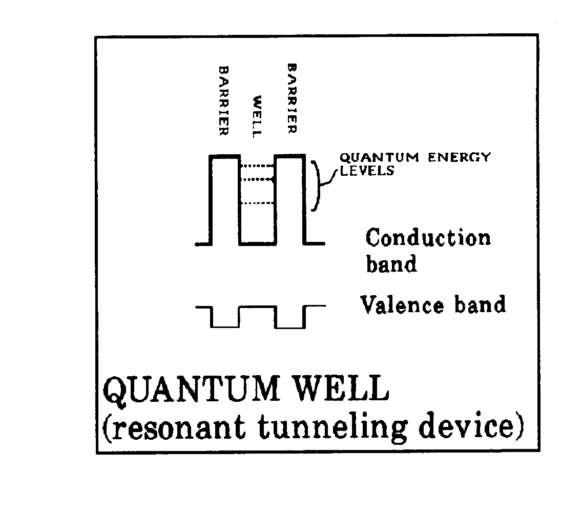
| |
| | |
| 15 | Superlattice: |
| | This subclass is indented under subclass 14. Subject matter wherein a large number of quantum wells are
present, the quantum wells being sufficiently close to each other
that carrier quantum wave functions are spread out over plural quantum
wells and the intervening barriers formed by the boundaries between adjacent
layers having different carrier affinities.
| | (1)
Note. Thicknesses of both the quantum well layers and the
barrier layers are typically a few angstroms to a few hundred angstroms
(10-10 meter) thick. |
| | (2)
Note. See the illustration, below, for energy level diagrams
showing band edge energy discontinuities at four types of superlattice
heterointerfaces.
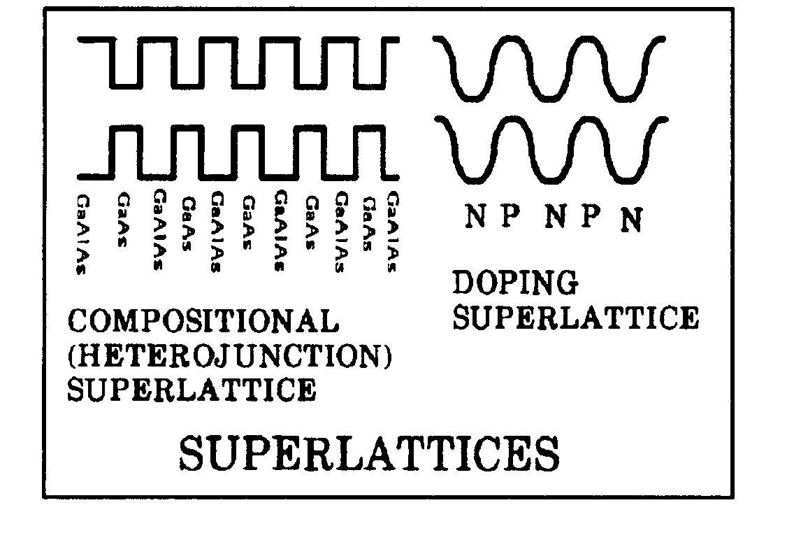
| SEE OR SEARCH CLASS:
| 148, | Metal Treatment, digest 160 for superlattice treatment. |
|
| | |
| 18 | Strained layer superlattice: |
| | This subclass is indented under subclass 15. Subject matter wherein the crystalline lattice characteristics
of adjacent thin active superlattice layers are mismatched so that
alternate layers are in elastic tension or compression. |
| | |
| 19 | SixGe1-x: |
| | This subclass is indented under subclass 18. Subject matter wherein at least one of the strained superlattice
materials is a silicon-germanium alloy. |
| | |
| 20 | Field effect device: |
| | This subclass is indented under subclass 15. Subject matter wherein the superlattice active layer forms
the conduction channel of a field effect device (i.e., one which
has two or more terminals denoted as source and gate with a conduction
channel therebetween, and in which the current through the conducting
channel is controlled by an electric field coming from a voltage
which is applied between the gate and source terminals thereof). |
| | |
| 21 | Light responsive structure: |
| | This subclass is indented under subclass 15. Subject matter wherein absorption of light (ultraviolet,
visible, or infrared) by a superlattice active layer or junction
causes a change in the current-voltage characteristic of the device. |
| | |
| 23 | Current flow across well: |
| | This subclass is indented under subclass 14. Subject matter wherein the device operation involves flow
of carriers (electrons or holes) across the quantum well (as contrasted
with tunneling through the well).
| | (1)
Note. Current flow is considered to be "across" the
well if the carriers have sufficient energy to pass over the barrier layers
confining the quantum well, as contrasted to passing through the
barriers by quantum mechanical tunneling. |
SEE OR SEARCH THIS CLASS, SUBCLASS:
| 25, | for devices which operate by resonant tunneling
through the barriers, rather than over them. |
|
| | |
| 24 | Field effect device: |
| | This subclass is indented under subclass 14. Subject matter wherein the quantum well device is a field
effect device, i.e., one which has two or more terminals denoted
as source and gate, with a conduction channel therebetween, and
in which the current through the conducting channel is controlled
by an electric field coming from a voltage which is applied between
the gate and source terminals thereof.
| | (1)
Note. See illustration under subclass 213 for various field
effect devices. | |
| | |
| 25 | Employing resonant tunneling: |
| | This subclass is indented under subclass 14. Subject matter wherein the operation of the device depends
not only on carrier charge confinement by the quantum well, but
the quantum well layer also acts as an intermediate layer through
which carriers pass by resonantly tunneling through both confining
barriers and the well. |
| | |
| 26 | Ballistic transport device: |
| | This subclass is indented under subclass 12. Subject matter in which an active layer is present through
which carriers pass, wherein the active layer is thinner than the
mean free path of the carriers in the material in that layer, so
that carriers can pass through the layer without scattering.
| | (1)
Note. Carriers are typically injected into the ballistic
transport layer as "hot" carriers, having an energy,
in the case of electrons, substantially greater than the minimum
of the conduction band, or in the case of holes, substantially lower than
the maximum of the valence band. | |
| | |
| 27 | Field effect transistor: |
| | This subclass is indented under subclass 26. Subject matter wherein the ballistic transport device is
a field effect transistor, i.e., one which has two or more terminals
denoted as source and gate with a conduction channel therebetween,
and in which the current through the conducting channel is controlled
by an electric field coming from a voltage which is applied between
the gate and source terminals thereof.
| | (1)
Note. See illustration, below, of various field effect devices
under subclass 213. | |
| | |
| 28 | Non-heterojunction superlattice (e.g., doping superlattice
or alternating metal and insulator layers): |
| | This subclass is indented under subclass 9. Subject matter wherein there are a plurality of active layers
and barrier regions, the active layers being sufficiently close
to each other that carrier quantum wave functions are spread out over
plural active layers and the intervening barriers, and wherein the
active layers and barrier regions do not form heterojunctions between
different semiconductor materials.
| | (1)
Note. Typically the active layers and barrier layers may
be doped with opposite conductivity type dopants. Thicknesses of
both the active layers and the barrier layers are typically a few
angstroms to a few hundred angstroms (10-10 meter)
thick. | |
| | |
| 29 | Ballistic transport device (e.g., hot electron transistor): |
| | This subclass is indented under subclass 9. Subject matter in which an active layer is present through
which carriers pass, which active layer is thinner than the mean
free path of the carriers in the material in that layer, so that
carriers can pass through the layer without scattering.
| | (1)
Note. Carriers are typically injected into the ballistic transport
layer as "hot" carriers, having an energy, in
the case of electrons, substantially greater than the minimum of
the conduction band, or in the case of holes, substantially lower than
the maximum of the valence band. | |
| | |
| 30 | Tunneling through region of reduced conductivity: |
| | This subclass is indented under subclass 9. Subject matter wherein the active layer through which carrier
tunnelling occurs has lower electrical conductivity than the material
adjacent thereto.
SEE OR SEARCH CLASS:
| 29, | Metal Working,
subclass 25.01 for methods of making barrier layer devices of
the metal-insulator-metal type. |
| 331, | Oscillators,
subclass 107 for superconductive element and tunneling element
oscillators. |
|
| | |
| 31 | Josephson: |
| | This subclass is indented under subclass 30. Subject matter wherein the device is of the form of a pair
of superconductive electrodes separated by a thin, less conductive,
portion, through which superconductive tunneling may occur.
SEE OR SEARCH CLASS:
| 29, | Metal Working,
subclass 25.01 for methods of making barrier layer devices possessing
a Josephson junction. |
| 216, | Etching a Substrate: Processes,
subclass 3 for Josephson Junction device manufacture involving
etching. |
| 505, | Superconductor Technology: Apparatus, Material,
Process,
subclass 1 for high temperature superconductor Josephson devices
with particular electrode materials and pertinent cross-reference
art collections, including subclasses 857+ for nonlinear solid-state
device, system, or circuit; and subclasses 873+ active
solid-state devices. |
|
| | |
| 33 | High temperature (i.e., >30° Kelvin): |
| | This subclass is indented under subclass 32. Subject matter wherein the device can operate at temperatures
above 30 degrees on the Kelvin temperature scale.
SEE OR SEARCH CLASS:
| 505, | Superconductor Technology: Apparatus, Material,
Process,
subclass 1 for high temperature superconductor materials and
devices. |
|
| | |
| 40 | ORGANIC SEMICONDUCTOR MATERIAL: |
| | This subclass is indented under the class definition. Subject matter comprising a semiconductor compound that
includes an organic material characterized by two or more carbon
atoms bonded together, one atom of carbon bonded to at least one
atom of hydrogen or halogen (i.e., chlorine, fluorine, bromine,
iodine), or one atom of carbon bonded to at least one atom of nitrogen
by a single or double bond.
| | (1)
Note. Certain compounds are exceptions to this rule, i.e.,
HCN, CN-CN, HNCO, HNCS, cyanogen halides, cyanamide, fulminic acid,
and metal carbides. These are not regarded as organic materials. |
| | (2)
Note. Graphite and diamond are not regarded as organic, since
they are not compounds; silicon carbide is not regarded as organic.
Active solid-state devices using silicon carbide or diamond as
the semiconductor are in subclass 77 of this class. |
| | (3)
Note. Organic insulating materials, as opposed to semiconducting
materials, do not go in this subclass. |
SEE OR SEARCH CLASS:
| 136, | Batteries: Thermoelectric and Photoelectric,
subclass 263 for photoelectric cells containing organic active material. |
| 260, | Chemistry of Carbon Compounds, and other classes which form integral parts of Class
260, appropriate subclasses for organic materials |
| 313, | Electric Lamp and Discharge Devices,
subclass 504 for solid-state organic phosphor material luminescent
devices. |
| 361, | Electricity: Electrical Systems and Devices,
subclass 527 for solid electrolytic capacitors containing an organic
salt. |
| 438, | Semiconductor Device Manufacturing: Process,
subclass 82 for processes of making a light responsive device
utilizing an organic semiconductor, and subclass 99 for methods of
making an electrical device utilizing as a semiconductor component
an organic semiconductor. |
|
| | |
| 41 | POINT CONTACT DEVICE: |
| | This subclass is indented under the class definition. Subject matter including a junction between a semiconductor
and a metallic element (e.g., wire) at a single point of contact therebetween. |
| | |
| 42 | SEMICONDUCTOR IS SELENIUM OR TELLURIUM IN ELEMENTAL FORM: |
| | This subclass is indented under the class definition. Subject matter including a semiconductor material comprised
of selenium or tellurium in elemental form (i.e., not in a compound).
SEE OR SEARCH CLASS:
| 430, | Radiation Imagery Chemistry: Process, Composition
or Product,
subclass 57.8 for electrophotographic plates containing selenium
or a selenium alloy. |
|
| | |
| 43 | SEMICONDUCTOR IS AN OXIDE OF A METAL (E.G., CuO, ZnO) OR
COPPER SULFIDE: |
| | This subclass is indented under the class definition. Subject matter wherein a semiconductor material includes
a metal oxide or copper sulfide.
| | (1)
Note. Those variable resistors known as "coherers" which
are active solid-state devices, and are
made of a metal oxide, are found in this subclass. |
SEE OR SEARCH THIS CLASS, SUBCLASS:
| 798, | for other active solid-state device type coherers. |
SEE OR SEARCH CLASS:
| 338, | Electrical Resistors,
subclasses 1 and 223+ for passive solid-state coherers. |
| 438, | Semiconductor Device Manufacturing: Process,
subclass 85 for processes of making a light responsive device
utilizing as the semiconductive component a metal oxide or copper sulfide
and subclasses 104 for methods of forming an electrical device utilizing
as a semiconductive component a metal oxide or copper sulfide. |
|
| | |
| 44 | WITH METAL CONTACT ALLOYED TO ELEMENTAL SEMICONDUCTOR TYPE PN
JUNCTION IN NONREGENERATIVE STRUCTURE: |
| | This subclass is indented under subclass 107. Subject matter under the class definition wherein the active
solid-state device has a pn junction formed by alloying one or
more impurity metal contacts to an elemental semiconductor, and
wherein the active solid-state device is not a
regenerative device of this class.
| | (1)
Note. The impurity metal contact alloys with a semiconductor
material to form a p-region or n-region, depending on the impurity
used. | |
| | |
| 46 | In pn junction tunnel diode (Esaki diode): |
| | This subclass is indented under subclass 44. Subject matter wherein the alloyed pn junction device
is a tunnel diode, i.e., wherein the active solid-state device includes
a heavily doped pn junction wherein conduction occurs through the
junction potential barrier due to a quantum mechanical effect even
though the carriers which tunnel through the potential barrier do
not have enough energy to overcome the barrier potential. |
| | |
| 47 | In bipolar transistor structure: |
| | This subclass is indented under subclass 44. Subject matter wherein the alloyed pn junction device is
a bipolar transistor, i.e., a transistor structure whose working
current passes through semiconductor material of both polarities
(p and n). |
| | |
| 48 | TEST OR CALIBRATION STRUCTURE: |
| | This subclass is indented under the class definition. Subject matter in which structures are provided on active
solid-state devices to permit or facilitate the measurement, test,
or calibration of the characteristics of the devices.
| | (1)
Note. Active solid-state device standards are also included
herein. |
SEE OR SEARCH CLASS:
| 324, | Electricity: Measuring and Testing,
subclass 158 for semiconductor device test apparatus and methods. |
| 438, | Semiconductor Device Manufacturing: Process, particularly
subclass 18 for methods under the class definition having
combined therewith a step of measuring an electrical condition utilizing
a test element. |
|
| | |
| 49 | NON-SINGLE CRYSTAL, OR RECRYSTALLIZED, SEMICONDUCTOR MATERIAL
FORMS PART OF ACTIVE JUNCTION (INCLUDING FIELD-INDUCED ACTIVE JUNCTION): |
| | This subclass is indented under the class definition. Subject matter wherein there is an active junction (e.g.,
a junction between dissimilar materials, or a junction induced by
an applied electric field, which exhibits non-linear current-voltage
characteristics) and at least part of the active junction is formed
by a semiconductor material in polycrystalline or amorphous form.
SEE OR SEARCH CLASS:
| 136, | Batteries: Thermoelectric and Photoelectric,
subclass 258 for photoelectric cells with polycrystalline or
amorphous semiconductor material. |
| 438, | Semiconductor Device Manufacturing: Process, particularly
subclass 96 and 482+ for methods of depositing amorphous
semiconductive material functioning as an active region for an electrical
device and subclasses 97 and 488+ for methods of depositing polycrystalline
semiconductive material functioning as an active region for an electrical
device. |
|
| | |
| 52 | Amorphous semiconductor material: |
| | This subclass is indented under subclass 49. Subject matter wherein the non-single crystal semiconductor
material is amorphous, i.e., non-crystalline in the sense that (1)
there is either complete disorder in the arrangement of atoms or
molecules of the material or (2) there is an absence of any long
range structural order that is detectable by electron or X-ray diffraction
patterns of the material.
SEE OR SEARCH THIS CLASS, SUBCLASS:
| 2, | through 5, for bulk effect switching in amorphous
material. |
| 16, | for superlattice quantum well heterojunction devices
of amorphous semiconductor material. |
| 646, | for amorphous semiconductor material coating to
control surface effects. |
SEE OR SEARCH CLASS:
| 136, | Batteries: Thermoelectric and Photoelectric,
subclass 258 for photoelectric cells with polycrystalline or
amorphous semiconductor material. |
| 438, | Semiconductor Device Manufacturing: Process, particularly
subclasses 482+ for methods for depositing amorphous semiconductor. |
|
| | |
| 53 | Responsive to nonelectrical external signals (e.g., light): |
| | This subclass is indented under subclass 52. Subject matter wherein the amorphous semiconductor active
junction generates an electrical signal when subjected to non-electrical (e.g.,
optical, thermal, or vibratory) signals.
SEE OR SEARCH CLASS:
| 430, | Radiation Imagery Chemistry: Process, Composition
or Product,
subclass 57.4 for electrophotographic plates containing amorphous
silicon. |
|
| | |
| 57 | Field effect device in amorphous semiconductor material: |
| | This subclass is indented under subclass 52. Subject matter wherein the amorphous semiconductor active
junction is a field effect device, i.e., one which has a conducting
channel and two or more electrodes, one of which is denoted a source
and the other a drain electrode, and in which the current through
the conducting channel is controlled by an electric field coming
from a voltage which is applied between the gate and source terminals
thereof.
| | (1)
Note. See illustration under subclass 213 for various field
effect devices. |
SEE OR SEARCH CLASS:
| 438, | Semiconductor Device Manufacturing: Process, particularly
subclasses 149+ for methods of forming a field effect transistor
on an insulating substrate or layer (e.g., SOS, SOI, etc.). |
|
| | |
| 58 | With impurity other than hydrogen to passivate dangling
bonds (e.g., halide): |
| | This subclass is indented under subclass 57. Subject matter wherein the semiconductor active junction
amorphous field effect device is doped with an impurity other than
hydrogen (e.g., a halide) for providing electrical stability by
completing chemical bonds between semiconductor atoms which were
not completed due to the amorphous nature of the semiconductor active
layer material. |
| | |
| 59 | In array having structure for use as imager or display,
or with transparent electrode: |
| | This subclass is indented under subclass 57. Subject matter wherein a plurality of semiconductor active
junction amorphous field effect devices are interconnected in a
monolithic chip device for generating an image of an object, light
from which is incident on the device, or for displaying signals
applied to the device, or having an electrode that transmits optical
radiation in the infrared, visible, or ultraviolet wavelength bands. |
| | |
| 62 | With impurity other than hydrogen to passivate dangling
bonds (e.g., halide): |
| | This subclass is indented under subclass 52. Subject matter wherein the semiconductor active junction
amorphous field effect device is doped with an impurity other than
hydrogen (e.g., a halide) for providing electrical stability by
completing chemical bonds between semiconductor atoms which were
not completed due to the amorphous nature of the semiconductor active
layer material. |
| | |
| 70 | Recrystallized semiconductor material: |
| | This subclass is indented under subclass 67. Subject matter wherein the combined device contains a non-single
semiconductor region of recrystallized material.
| | (1)
Note. Recrystallized semiconductor material has been processed,
typically by heat or laser irradiation to cause growth of large
regions of substantially single crystal material to obtain properties approximating
those of completely single crystal material. | |
| | |
| 72 | In array having structure for use as imager or display,
or with transparent electrode: |
| | This subclass is indented under subclass 66. Subject matter wherein a plurality of field effect devices
in non-single crystal, or recrystallized, semiconductor material
are interconnected in a monolithic chip device for generating an
image of an object, light from which is incident on the device,
or for displaying signals applied to the device, or having an electrode
that transmits optical radiation in the infrared, visible, or ultraviolet
wavelength bands. |
| | |
| 76 | SPECIFIED WIDE BAND GAP (1.5eV) SEMICONDUCTOR MATERIAL
OTHER THAN GaAsP or GaAlAs: |
| | This subclass is indented under the class definition. Subject matter including a semiconductor material with a
band gap (between its valance and conduction bands) greater that
1.5 electron volts which is not gallium arsenide phosphide or gallium
aluminum arsenide. |
| | |
| 78 | II-VI compound: |
| | This subclass is indented under subclass 76. Subject matter wherein the specified wide band gap material
is a compound, one element of which comes from group II, and the
other element of which comes from group VI of the periodic table
of elements. |
| | |
| 79 | INCOHERENT LIGHT EMITTER STRUCTURE: |
| | This subclass is indented under the class definition. Subject matter wherein the active solid-state device generates
incoherent light when subjected to an appropriate input signal.
| | (1)
Note. Lasers (coherent light generators) are classified in
Class 372, and patents directed to lasers are not to be cross-referenced
in this or indented subclasses unless such patent contains disclosure
of a light emitting semiconductor device which is NOT a laser or
coherent light generator. |
SEE OR SEARCH THIS CLASS, SUBCLASS:
| 13, | for incoherent thin physical layer light emitter
devices with operating principles as specified therein. |
SEE OR SEARCH CLASS:
| 250, | Radiant Energy,
subclasses 552+ for solid-state light source circuits. |
| 313, | Electric Lamp and Discharge Devices,
subclasses 498+ for electric lamp and discharge devices having solid-state
luminescent materials, including nominally recited luminescent semiconductor
type materials; and subclass 504 for solid-state organic phosphor
material luminescent devices. |
| 340, | Communications: Electrical,
subclasses 760+ and 766+ for solid-state light emitting
arrays and array elements. |
| 362, | Illumination,
subclass 84 for light source or light source support and luminescent
material and subclass 800 (cross-reference art collection) for light
emitting diode light sources. |
| 438, | Semiconductor Device Manufacturing: Process, particularly
subclasses 22+ for methods of forming a semiconductor device which
may be emissive of either coherent or incoherent radiation. |
|
| | |
| 80 | In combination with or also constituting light responsive
device: |
| | This subclass is indented under subclass 79. Subject matter wherein the light emitting active semiconductor
device is combined with a separate device which generates an electrical
signal when light impinges upon it or the active device both emits
light when stimulated and generates an electrical signal in response
to light impingent thereupon.
SEE OR SEARCH CLASS:
| 250, | Radiant Energy,
subclass 551 for signal isolators involving a light source and
photodetector. |
|
| | |
| 83 | Light coupled transistor structure: |
| | This subclass is indented under subclass 80. Subject matter wherein the active solid-state device has
a pair of rectifying junctions, a first of which when forward biased
produces light which, when absorbed in the depletion region of the
second junction when reverse biased, produces a current through
the second junction, with the first junction functioning similarly
to the emitter-base junction, and the second junction functioning
similarly to the base-collector junction, of an ordinary bipolar
transistor.
SEE OR SEARCH CLASS:
| 250, | Radiant Energy,
subclass 551 for signal isolator for optically coupled light emitter
and light detector combinations wherein the devices are used to isolate
electrical signals. |
|
| | |
| 85 | With heterojunction: |
| | This subclass is indented under subclass 84. Subject matter wherein the device contains a heterojunction,
i.e., wherein the junction separates semiconductor materials of
different chemical composition. |
| | |
| 86 | Active layer of indirect band gap semiconductor: |
| | This subclass is indented under subclass 79. Subject matter wherein the light emitting active region
is in or between semiconductor materials in which direct transitions
of electrons from conduction to valance bands do not take place.
| | (1)
Note. Transitions may take place in steps due to trapping
levels located in the forbidden band between the conduction and
valance bands. | |
| | |
| 90 | With heterojunction: |
| | This subclass is indented under subclass 89. Subject matter wherein there is at least one heterojunction,
i.e., wherein the junction separates semiconductor materials of
different chemical composition. |
| | |
| 91 | With shaped contacts or opaque masking: |
| | This subclass is indented under subclass 88. Subject matter wherein the plural light emitting devices
have electrical contacts with specific shapes or are combined with
optical elements which are impervious to light emitted by the devices
and are placed in the path of light emitted by the devices. |
| | |
| 92 | Alphanumeric segmented array: |
| | This subclass is indented under subclass 88. Subject matter wherein the plural light emitting devices
are structured and arranged in segments of Arabic numerals or alphabet
letters.
SEE OR SEARCH CLASS:
| 340, | Communications: Electrical,
subclasses 760+ and 766+ for solid-state light emitting
arrays and array elements. |
|
| | |
| 94 | With heterojunction: |
| | This subclass is indented under subclass 79. Subject matter wherein there is at least one junction between
semiconductor materials of different chemical compositions.
| | (1)
Note. See the illustration of a heterojunction device in
subclass 183. | |
| | |
| 98 | With reflector, opaque mask, or optical element (e.g.,
lens, optical fiber, index of refraction matching layer, luminescent material
layer, filter) integral with device or device enclosure or package: |
| | This subclass is indented under subclass 79. Subject matter wherein the light emitting active junction
device is combined with one or more optical elements (e.g., to transmit
or shape or otherwise affect light emitted by the device); and the
optical element is an integral part of the device or of the housing,
encapsulant, or other device enclosure or package. |
| | |
| 100 | Encapsulated: |
| | This subclass is indented under subclass 79. Subject matter wherein the light emitting active junction
device is embedded in a protective coating.
SEE OR SEARCH CLASS:
| 174, | Electricity: Conductors and Insulators,
subclass 521 for potted or encapsulated electrical devices. |
| 439, | Electrical Connectors,
subclass 936 for potting material or coating for electrical
conductors. |
|
| | |
| 104 | TUNNELING PN JUNCTION (E.G., ESAKI DIODE) DEVICE: |
| | This subclass is indented under the class definition. Subject matter wherein the active solid-state device includes
a heavily doped pn junction where conduction occurs through the
junction potential barrier due to a quantum mechanical effect even
though the carriers which tunnel through the potential barrier do not
have enough energy to overcome the barrier potential.
| | (1)
Note. PN Junction tunnel diodes operated under forward bias
are often referred to as Esaki diodes. |
SEE OR SEARCH THIS CLASS, SUBCLASS:
| 46, | for an Esaki diode having a metal contact alloyed
to elemental semiconductor type pn junction in a non-regenerative
structure. |
SEE OR SEARCH CLASS:
| 326, | Electronic Digital Logic Circuitry,
subclass 134 for a digital logic device which includes a tunnel
diode. |
| 327, | Miscellaneous Active Electrical Nonlinear Devices,
Circuits, and Systems,
subclass 195 for stable state circuits utilizing a tunnel diode;
subclass 326 for limiting, clipping, or clamping using a tunnel
diode; subclass 402 for a delay controlled switch with tunnel diode;
subclasses 420 and 499 for gating circuits utilizing transistors
or diodes respectively which use tunnel diodes; and subclass 570
for miscellaneous tunnel diode circuits. |
| 331, | Oscillators,
subclass 107 for tunnel diode oscillators. |
| 361, | Electricity: Electrical Systems and Devices,
subclass 100 for tunnel diode current responsive fault sensors. |
|
| | |
| 105 | In three or more terminal device: |
| | This subclass is indented under subclass 104. Subject matter wherein the tunnel junction is part of an
active solid-state electronic device which has three or more electrical
terminals (e.g., transistors or thyristors). |
| | |
| 106 | Reverse bias tunneling structure (e.g., "backward" diode,
true Zener diode): |
| | This subclass is indented under subclass 104. Subject matter wherein the tunnel junction is structured
to permit quantum mechanical tunneling of carriers in a reverse
bias mode, i.e., when the p-side of the junction is connected to a
negative voltage source and the n-side of the junction is connected
to a positive voltage source.
| | (1)
Note. In silicon, such conduction occurs when the junction
breakdown voltage is less than approximately 5.6 volts. |
SEE OR SEARCH CLASS:
| 148, | Metal Treatment, digest 174 for treatment of Zener diodes. |
| 323, | Electricity: Power Supply or Regulation Systems,
subclass 231 for systems using a Zener diode and being in shunt
with a load. |
| 327, | Miscellaneous Active Electrical Nonlinear Devices,
Circuits, and Systems,
subclasses 194 and 195 for stable state circuits with a zener
or back diode respectively; subclass 326 for limiting, clipping,
or clamping utilizing a zener diode; subclass 421 for gating circuits
having a transistor which utilizes a zener effect; subclass 502
for a gating circuit with zener diode; and subclass 584 for a miscellaneous
circuit utilizing a zener diode. |
| 361, | Electricity: Electrical Systems and Devices,
subclass 197 , for relay time delay safety or protection devices including,
for example, a Zener diode. |
| 377, | Electrical Pulse Counters, Pulse Dividers, or
Shift Registers: Circuits and Systems,
subclass 128 for pulse counting or dividing chains which include
bi-stable semiconductor devices with only two electrodes, e.g., tunnel
diodes. |
|
| | |
| 107 | REGENERATIVE TYPE SWITCHING DEVICE (E.G., SCR, COMFET,
THYRISTOR): |
| | This subclass is indented under the class definition. Subject matter wherein the active solid-state device acts
as if it has two or more active emitter junctions each of which
is associated with a separate, equivalent transistor having an individual
gain and, when initiated by a base region current, the equivalent
transistors mutually drive each other in a regenerative manner to
lower the voltage drop between the emitters.
| | (1)
Note. If the current is above a level IH, called
the "holding current", then the device will remain
ON when the triggering signal is removed by the regenerative feedback
therebetween, and is then said to be "latched". |
SEE OR SEARCH CLASS:
| 123, | Internal-Combustion Engines,
subclass 648 for circuits employing silicon controlled rectifiers
(SCRs). |
| 327, | Miscellaneous Active Electrical Nonlinear Devices,
Circuits, and Systems,
subclasses 199+ for a bistable circuit which includes diverse solid-state devices
such as an SCR, subclasses 392+ for a delay controlled
switch which may include an SCR, and subclasses 438+ for
gating circuits which may use a thyristor or SCR. |
| 361, | Electricity: Electrical Systems and Devices,
subclasses 100+ and 205 for circuits employing thyristors (e.g.,
silicon controlled rectifiers (SCRs)). |
| 363, | Electric Power Conversion Systems,
subclasses 27+ , 54, 57+, 68, 85+, 96+,
128+, 135+, and 160+ for circuits employing
thyristors (e.g., silicon controlled rectifiers (SCRs)). |
| 388, | Electricity: Motor Control Systems,
subclasses 917+ for circuits employing thyristors (e.g., silicon
controlled rectifiers (SCRs)). |
| 438, | Semiconductor Device Manufacturing: Process, particularly
subclasses 133+ for methods of forming a regenerative type switching
device. |
|
| | |
| 111 | Triggered by VBO overvoltage means: |
| | This subclass is indented under subclass 109. Subject matter wherein the two terminal device with no control
electrode includes means to apply a voltage larger than the breakover
voltage VBO to initiate operation of the device. |
| | |
| 113 | With light activation: |
| | This subclass is indented under subclass 107. Subject matter wherein the regenerative switching device
is activated (e.g., turned on and/or off) by light impinging
on a light sensitive portion of the device. |
| | |
| 118 | With groove or thinned light sensitive portion: |
| | This subclass is indented under subclass 113. Subject matter wherein the light sensitive portion is located
in a groove in the surface of the device or is located close to
the surface of the device in a thinned region of the device so that only
a relatively thin portion of the device has to be traversed by light. |
| | |
| 119 | Bidirectional rectifier with control electrode (gate) (e.g.,
Triac): |
| | This subclass is indented under subclass 107. Subject matter wherein the regenerative switching device
has a control electrode, can conduct in both forward and reverse
directions, and can be triggered into conduction by a pulse applied
to its control electrode.
SEE OR SEARCH THIS CLASS, SUBCLASS:
| 110, | for bidirectional rectifiers with no control electrode. |
SEE OR SEARCH CLASS:
| 323, | Electricity: Power Supply or Regulation Systems,
subclasses 240 and 325 for circuit having unidirectional elements
with bidirectional pass. |
|
| | |
| 121 | With diode or transistor in reverse path: |
| | This subclass is indented under subclass 119. Subject matter wherein a diode (i.e., a device which passes
current in only one direction) is connected to conduct current in
one direction, with a regenerative switching device with a control
electrode connected to conduct current in the other direction to
produce a bi-directionally conducting regenerative switching device. |
| | |
| 122 | Lateral: |
| | This subclass is indented under subclass 119. Subject matter wherein the bidirectional rectifier with
control electrode is of the lateral type, i.e., when viewed in cross
section, the two main electrodes (e.g., anode and cathode) are arranged
horizontally, side-by-side in the same surface of the semiconductor
body. |
| | |
| 124 | Combined with field effect transistor structure: |
| | This subclass is indented under subclass 119. Subject matter wherein the bidirectional rectifier with
control electrode includes or is combined with a field effect transistor
structure, i.e., a transistor in which the current through a conducting
channel is controlled by an electric field coming from a voltage
which is applied between the gate and source terminals thereof.
| | (1)
Note. See illustration under subclass 213 for various field
effect devices. | |
| | |
| 125 | Controllable emitter shunting: |
| | This subclass is indented under subclass 124. Subject matter wherein the field effect transistor structure
is connected to shunt one of the emitter-base junctions of the regenerative structure
under control of the voltage applied to the gate of the field effect
transistor. |
| | |
| 127 | Guard ring or groove: |
| | This subclass is indented under subclass 126. Subject matter wherein the means to separate portions of
the device having different conductive polarity is or includes a
groove, or a guard ring, i.e., a pn junction region in the body
of the device located and/or configured to reduce electric
field strength at a given applied voltage. |
| | |
| 131 | Recombination centers or deep level dopants: |
| | This subclass is indented under subclass 130. Subject matter wherein the switching speed enhancement means
include (1) centers wherein excess holes and electrons recombine and
are removed as charge carriers in the device or (2) dopant ions
with energy levels that are located in the forbidden band of the active
semiconductor material of the device. |
| | |
| 132 | Five or more layer unidirectional structure: |
| | This subclass is indented under subclass 107. Subject matter wherein the regenerative active solid-state
device has five or more layers of semiconductor material producing
at least four active junctions, and is operable in a single electrical
direction. |
| | |
| 133 | Combined with field effect transistor: |
| | This subclass is indented under subclass 107. Subject matter wherein the regenerative device includes
or is combined with a field effect transistor, i.e., a transistor
in which the current through a conducting channel is controlled
by an electric field coming from a voltage which is applied between
the gate and source terminals thereof. |
| | |
| 134 | J-FET (junction field effect transistor): |
| | This subclass is indented under subclass 133. Subject matter wherein the field effect transistor combined
with the regenerative action junction type switching device is a
junction field effect transistor, i.e., a field effect transistor wherein
the gate region is isolated from the conducting channel by a rectifying
pn junction or Schottky barrier junction.
SEE OR SEARCH THIS CLASS, SUBCLASS:
| 287, | for power JFET devices. |
| 504, | for JFET type isolation. |
|
| | |
| 136 | Enhancement mode (e.g., so-called SITs): |
| | This subclass is indented under subclass 135. Subject matter in which no current flows except for leakage
current, when the gate to source voltage is zero.
| | (1)
Note. Conduction does not begin until the gate voltage reaches
a finite threshold value. |
| | (2)
Note. Compare this with depletion mode J-FETS in which maximum
current is passed by the transistor at a zero gate potential and
current decreases as the gate voltage increases. | |
| | |
| 137 | Having controllable emitter shunt: |
| | This subclass is indented under subclass 133. Subject matter wherein the regenerative switching device
is combined with a junction field effect transistor that is connected
across an emitter-base junction of the regenerative device to controllably
divert current from the emitter-base junction. |
| | |
| 142 | Having impurity doping for gain reduction: |
| | This subclass is indented under subclass 139. Subject matter wherein the extended latchup current level
device has impurity dopant to reduce device regenerative gain, i.e.,
the gain or amplification of one or more of the active junction
portions connected in regenerative fashion. |
| | |
| 143 | Having anode shunt means: |
| | This subclass is indented under subclass 139. Subject matter wherein the extended latchup current level
device has means connected across the emitter-base junction of the
PNP transistor portion of the regenerative device to controllably
divert current from the emitter-base junction. |
| | |
| 145 | Low impedance channel contact extends below surface: |
| | This subclass is indented under subclass 139. Subject matter wherein the extended latchup current level
device has an electrical contact extending from the device surface
into the body of the device which is connected to the channel of
the field effect transistor portion and wherein the contact has
a relatively low electrical impedance. |
| | |
| 148 | Having impurity doping for gain reduction: |
| | This subclass is indented under subclass 147. Subject matter wherein the regenerative switching device
has impurity dopant to reduce device gain of one of the equivalent
transistors.
SEE OR SEARCH THIS CLASS, SUBCLASS:
| 142, | for this subject matter in a COMFET device. |
|
| | |
| 149 | Having anode shunt means: |
| | This subclass is indented under subclass 147. Subject matter wherein the regenerative switching device
has means connected across the emitter-base junction of the PNP
transistor section of the regenerative device to divert current
from the emitter-base junction. |
| | |
| 156 | Having deep level dopants or recombination centers: |
| | This subclass is indented under subclass 155. Subject matter wherein the regenerative device has deep
level dopants or electron-hole recombination centers with energy
levels that are within the forbidden energy band and widely spaced
from the conduction and valence bands of the semiconductor device. |
| | |
| 157 | With integrated trigger signal amplification means (e.g.,
amplified gate, "pilot thyristor", etc.): |
| | This subclass is indented under subclass 107. Subject matter wherein the regenerative switching device
has means to amplify the control current of the device, which is
physically integrated with the regenerative switching device.
SEE OR SEARCH THIS CLASS, SUBCLASS:
| 115, | for light activated regenerative devices with trigger
signal amplification. |
| 123, | for bidirectional regenerative devices with trigger
signal amplification. |
SEE OR SEARCH CLASS:
| 330, | Amplifiers,
subclasses 250+ for semiconductor amplifying devices (e.g., transistors |
|
| | |
| 159 | Transistor as amplifier: |
| | This subclass is indented under subclass 157. Subject matter wherein the amplification means is a transistor
(i.e., an active semiconductor device having three or more electrodes). |
| | |
| 160 | With distributed amplified current: |
| | This subclass is indented under subclass 157. Subject matter wherein the regenerative device with amplification
means produces amplified current which is distributed by electrodes
to other portions of the device. |
| | |
| 161 | With a turn-off diode: |
| | This subclass is indented under subclass 157. Subject matter wherein the regenerative device with amplification
means is integrally provided with a diode, i.e., a solid-state active
rectifying two terminal device, to bypass the amplifying stage(s),
in order to switch OFF the regenerative device. |
| | |
| 162 | Lateral structure: |
| | This subclass is indented under subclass 107. Subject matter wherein the regenerative active junction
type switching device has a lateral structure, i.e., one in which
the active junctions are arranged so that electric current flows
from side to side, rather than from top to bottom of the device. |
| | |
| 163 | Emitter region feature: |
| | This subclass is indented under subclass 107. Subject matter wherein the active emitter junction region
of the regenerative device has a particular characteristic. |
| | |
| 166 | Radially symmetric regions: |
| | This subclass is indented under subclass 164. Subject matter wherein the plural emitters are located in
regions of the device which are symmetrical extending radially in
a horizontal direction from a predetermined emitter location. |
| | |
| 169 | High resistivity base layer: |
| | This subclass is indented under subclass 168. Subject matter wherein the means for increasing breakdown
voltage includes a base (as contrasted with emitter or collector)
layer which has a relatively high electrical resistivity. |
| | |
| 172 | With means to lower "ON" voltage drop: |
| | This subclass is indented under subclass 107. Subject matter wherein the regenerative active junction
type switching device comprises means to lower the voltage drop
across the main terminals when the switch is operated in the ON
mode. |
| | |
| 173 | Device protection (e.g., from overvoltage): |
| | This subclass is indented under subclass 107. Subject matter wherein the regenerative active junction
type switching device includes means for protecting the device from
destructive overloads (e.g., from operating voltage above a particular
threshold level).
SEE OR SEARCH CLASS:
| 361, | Electricity: Electrical Systems and Devices,
subclasses 91.1+ for overvoltage protection in safety and protection
of systems and devices. |
|
| | |
| 175 | With means to control triggering (e.g., gate electrode
configuration, Zener diode firing, dV/Dt control, transient
control by ferrite bead, etc.): |
| | This subclass is indented under subclass 107. Subject matter wherein the regenerative active junction
type switching device includes means for controlling device turn-on.
| | (1)
Note. Transient electrical phenomena, e.g., damped oscillations
or surges in operation current or voltage following a sudden change
in the applied voltage or current to the device, may be controlled, for
example, by use of ferrite bead or capacitive input means. | |
| | |
| 177 | With housing or external electrode: |
| | This subclass is indented under subclass 107. Subject matter wherein the regenerative active junction
type switching device includes a structure in which to place the
device.
SEE OR SEARCH THIS CLASS, SUBCLASS:
| 81, | and 82, for a light emitting device in combination
with or constituting a light responsive device, with specific housing
structure. |
| 99, | for light emitting device with specific housing
structure. |
| 433, | and 434, for light responsive device with housing
or encapsulation means. |
| 573, | for Darlington configuration bipolar transistor
structure with housing or contact structure. |
| 584, | for enlarged emitter device bipolar transistor means
having housing or contact. |
| 602, | for a voltage variable capacitance device with specified
housing or contact. |
| 660, | for means to shield a device contained in a housing. |
|
| | |
| 180 | Stud mount: |
| | This subclass is indented under subclass 177. Subject matter wherein the housing is provided with a threaded
or serrated insert or post used for connecting heat sinks or terminals
to the device. |
| | |
| 183 | HETEROJUNCTION DEVICE: |
| | This subclass is indented under the class definition. Subject matter wherein the active solid-state device contains
a heterojunction, i.e., a boundary between different regions, one
of which is made of a material that differs from that of the other
region.
| | (1)
Note. See illustration, below, for an example of a heterojunction
bipolar transistor.
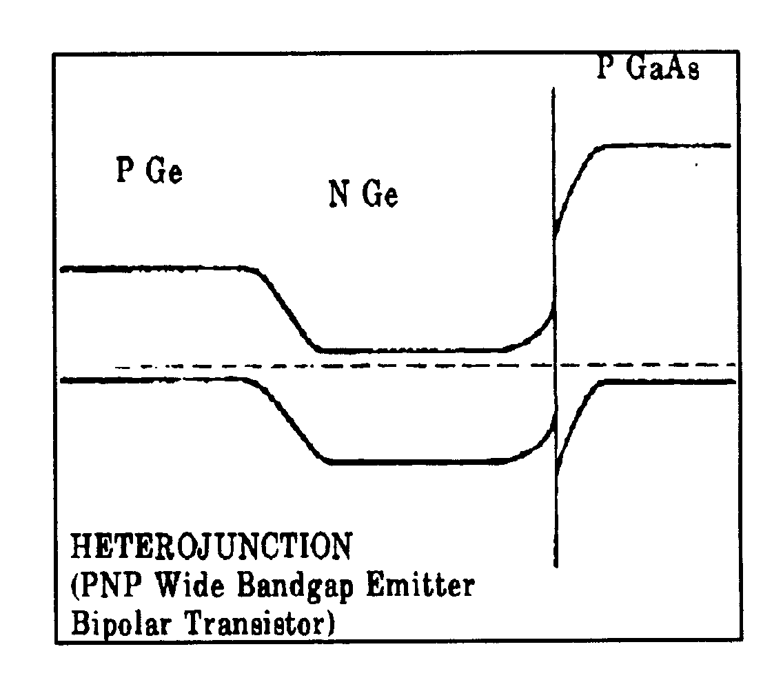
| SEE OR SEARCH THIS CLASS, SUBCLASS:
| 10, | and 11, for a heterojunction involving a low workfunction
layer for electron emission. |
| 12, | through 27, for heterojunction devices which involve
quantum well, superlattice or ballistic (hot carrier) transport
devices. |
| 51, | for a non-single crystal material/monocrystal
heterojunction device. |
| 85, | for a light emitting structure device combined with
a light responsive device in an integrated structure wherein the
light responsive device has a heterojunction. |
| 90, | for plural light emitting heterojunction devices. |
| 94, | through 97, for heterojunction light emitter structures. |
| 183.1, | for a heterojunction charge transfer device. |
SEE OR SEARCH CLASS:
| 372, | Coherent Light Generators,
subclasses 43 through 50for semiconductor lasers which may contain heterojunctions. |
|
| | |
| 183.1 | Charge transfer device: |
| | This subclass is indented under subclass 183. Subject matter in which storage sites for packets of electric
charge are induced at or below the surface of the active solid-state
(semiconductor) device by an electric field applied to the device
and wherein carrier potential energy per unit charge minima is established
at a given storage site and such minima is transferred to one or
more adjacent storage sites in a serial manner and which contains
a junction between two semiconductor materials of different chemical
compositions each different composition having a different carrier
affinity.
| | (1)
Note. Typically, heterojunctions are between materials which
additionally have different band gaps, but that is not true of all
heterojunctions. |
SEE OR SEARCH THIS CLASS, SUBCLASS:
| 215, | for charge transfer devices which do not involve
heterojunctions. |
|
| | |
| 185 | Staircase (including graded composition) device: |
| | This subclass is indented under subclass 184. Subject matter wherein the active region contains a number
of layers forming plural heterojunctions and the carrier (i.e.,
electron or hole) affinities of each layer incrementally increase or
decrease progressively across the active region thickness, so that
the energy level diagram of the active region, when under electrical
bias, resembles a staircase.
| | (1)
Note. Staircase effect devices may also be provided with
a graded composition, i.e., wherein the chemical composition of
the semiconductor forming the heterojunction varies in a direction
either perpendicular or parallel to the junction. |
| | (2)
Note. See illustration, below, for an example of a staircase
bandgap.
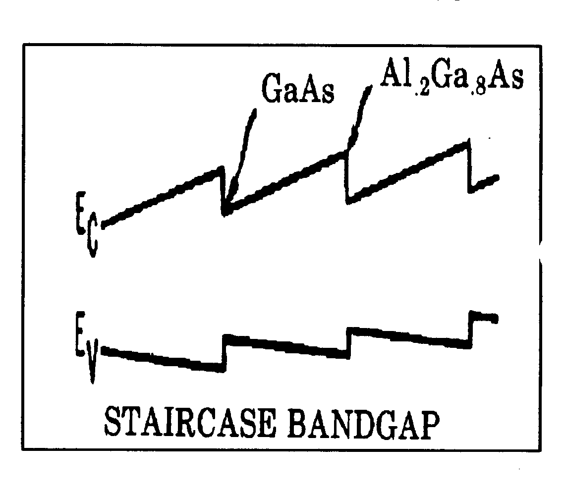
| |
| | |
| 186 | Avalanche photodetection structure: |
| | This subclass is indented under subclass 184. Subject matter wherein carriers generated in the active
region of the device in response to light incident thereupon, achieve
enough kinetic energy to knock further carriers from the crystalline
lattice of the active region producing an avalanche or snowball
increase in operating current level.
| | (1)
Note. Avalanche photodetector devices may have bipolar transistor
structure, i.e., wherein the heterojunction device has three terminals
- an emitter, a collector and a base, the operating current comprising
both positive and negative electrical charges. | |
| | |
| 187 | Having transistor structure: |
| | This subclass is indented under subclass 184. Subject matter wherein the light responsive heterojunction
device has three terminals - an emitter, collector, and a base;
a source, drain, and gate; or a hybrid combination of each, which
can provide gain or can be used as a switch. |
| | |
| 189 | Layer is a group III-V semiconductor compound: |
| | This subclass is indented under subclass 188. Subject matter wherein the narrow energy band gap layer
is a semiconductor compound made of one element taken from periodic
table group III elements and another element taken from periodic
table group V elements. |
| | |
| 190 | With lattice constant mismatch (e.g., with buffer layer
to accommodate mismatch): |
| | This subclass is indented under subclass 183. Subject matter wherein at least one of the materials that
form the heterojunction has a crystalline lattice constant which
is made to differ from the lattice constant of the other material which
forms the heterojunction.
| | (1)
Note. Typically, lattice mismatches are sought to be avoided.
However, sometimes they are desired, as for example, when the resulting
strain favorably affects the properties of the strained semiconductor. |
| | (2)
Note. A buffer layer may be provided to accommodate a lattice
mismatch, i.e., a layer of material which mechanically separates
the layers which have different lattice constants. |
SEE OR SEARCH THIS CLASS, SUBCLASS:
| 18, | for strained layer heterojunctions in a superlattice. |
|
| | |
| 191 | Having graded composition: |
| | This subclass is indented under subclass 183. Subject matter wherein the chemical composition of the semiconductor
forming the heterojunction varies continuously in a direction either
perpendicular or parallel to the junction. |
| | |
| 192 | Field effect transistor: |
| | This subclass is indented under subclass 183. Subject matter wherein the heterojunction is part of a field
effect transistor, i.e., wherein the current through the active
heterojunction is controlled by a voltage applied between gate and
source terminals of the device. |
| | |
| 194 | Doping on side of heterojunction with lower carrier affinity
(e.g., high electron mobility transistor (HEMT)): |
| | This subclass is indented under subclass 192. Subject matter wherein the heterojunction field effect transistor
has impurity dopant on the side of the heterojunction with lower
affinity for the charge carriers (holes or electrons)
supplied by the dopant, so that the charge carriers spill over the
heterojunction into the side with higher carrier affinity.
| | (1)
Note. Typically, the spilled over charge carriers constitute
the conductive channel connecting the source and drain electrodes. |
| | (2)
Note. Such devices may be provided with a channel layer of
semiconductor material other than group III-V compound semiconductor
(e.g., IV-VI compound semiconductor, germanium semiconductor, etc.). |
SEE OR SEARCH THIS CLASS, SUBCLASS:
| 12, | through 27, for other closely related quantum well
and ballistic transport field effect devices. |
|
| | |
| 195 | Combined with diverse type device: |
| | This subclass is indented under subclass 194. Subject matter wherein the heterojunction field effect transistor
with impurity dopant on the side of the heterojunction with lower
affinity for the charge carriers supplied by the dopant is combined
with another electronic device.
| | (1)
Note. Typical diverse devises include complementary field
effect transistors, i.e., a field effect transistor of opposite conductivity
type to the heterojunction field effect transistor; and field effect transistors
of different threshold voltages (e.g., enhancement and depletion HEMTs
in same integrated circuit). | |
| | |
| 197 | Bipolar transistor: |
| | This subclass is indented under subclass 183. Subject matter wherein the heterojunction is part of a bipolar
transistor, i.e., a transistor structure whose working current passes through
semiconductor material of both polarities (p and n) which form a
heterojunction portion of the transistor.
SEE OR SEARCH CLASS:
| 438, | Semiconductor Device Manufacturing: Process, particularly
subclasses 312+ for methods of forming a heterojunction bipolar
transistor. |
|
| | |
| 198 | Wide band gap emitter: |
| | This subclass is indented under subclass 197. Subject matter wherein the bipolar transistor with an active
heterojunction region involves a charge carrier emitter region made
of a semiconductor material having an energy gap between its conduction
and valence bands which is greater than the energy gap of the base region
forming a heterojunction therewith. |
| | |
| 199 | Avalanche diode (e.g., so-called "Zener" diode
having breakdown voltage greater than 6 volts, including heterojunction IMPATT
type microwave diodes): |
| | This subclass is indented under subclass 183. Subject matter wherein the heterojunction device is a diode
in which conduction under reverse bias conditions is caused by avalanche
breakdown at an applied voltage greater than 6 volts.
| | (1)
Note. One example of such a device is a microwave transit
time device (e.g., IMPATT diode). |
SEE OR SEARCH THIS CLASS, SUBCLASS:
| 481, | for a Schottky barrier avalanche diode. |
| 551, | for an avalanche diode used as a voltage reference
element combined with pn junction isolation means in an integrated
circuit. |
| 603, | through 606, for avalanche diodes not classified
above those subclasses in this schedule, i.e., not involving a heterojunction
in a non-charge transfer device, or a Schottky barrier, or one used
as a voltage reference element with pn junction isolation means
in an integrated circuit. |
SEE OR SEARCH CLASS:
| 331, | Oscillators,
subclasses 107+ for solid-state active element oscillators. |
|
| | |
| 202 | GATE ARRAYS: |
| | This subclass is indented under the class definition. Subject matter comprising a repeating geometric arrangement
of individual structural units of solid-state devices, the solid-state devices
of each individual structural unit being connectable into various
different types of logic circuits in one integrated, monolithic chip.
| | (1)
Note. The significant distinction between a "gate
array" and other arrays of active solid state devices,
such as read-only memories (ROMs), and programmable logic arrays
(PLAs), is that the solid-state devices of each individual structural
of a "gate array" can be connected into various
different types of logic circuits, whereas in a ROM or PLA, each
of the individual structural units is configured so that they must
be connected into the same type of logic circuit (e.g., wherein
all individual structural units are connected as NOR gates). |
SEE OR SEARCH CLASS:
| 438, | Semiconductor Device Manufacturing: Process, particularly
subclasses 128+ for methods of forming an array of devices upon
a semiconductor substrate and selectively interconnecting the same. |
|
| | |
| 203 | With particular chip input/output means: |
| | This subclass is indented under subclass 202. Subject matter wherein the gate array integrated circuit
is provided with specific means to input and output electrical signals
to operate the device.
| | (1)
Note. Examples of particular chip input/output means
include (a) interface circuits, i.e., circuits that connect the
chip to another device or to a circuit and which produces necessary
current and voltage characteristics for the interconnected devices
and circuits to function properly, with particular active solid-state
devices used in the interface circuits; (b) structure permitting
electrical interconnection to either receive an input signal or
to output an output signal; or (c) specific bonding pad or electrode configurations
(i.e., wherein the input/output means includes a particular
electrically conductive surface to which electrical interconnecting
element (e.g., electrical leads) can be connected, or has a specified
electrode configuration such as a power supply bus for the input/output
means separate from those used to power the gate array devices. | |
| | |
| 210 | With wiring channel area: |
| | This subclass is indented under subclass 208. Subject matter wherein the signal paths in the array are
located in an area separate from the active devices forming the
elements of the array. |
| | |
| 211 | Multi-level metallization: |
| | This subclass is indented under subclass 208. Subject matter wherein the particular signal path connections
include more than one layer of conductive metal deposited on a substrate.
| | (1)
Note. The multilayer metallization may include a layer of
material made up of silicon in polycrystalline form or a silicide
compound. | |
| | |
| 212 | CONDUCTIVITY MODULATION DEVICE (E.G., UNIJUNCTION TRANSISTOR,
DOUBLE-BASE DIODE, CONDUCTIVITY-MODULATED TRANSISTOR): |
| | This subclass is indented under the class definition. Subject matter wherein the active solid-state device has
a high resistivity semiconductor region of one conductivity type
having a region of opposite conductivity type forming a pn junction
with a central portion of the high resistivity layer, with structural
means provided to forward bias the pn junction to inject minority
carriers into the high resistivity region to increase its conductivity
through conductivity modulation.
SEE OR SEARCH CLASS:
| 327, | Miscellaneous Active Electrical Nonlinear Devices,
Circuits, and Systems,
subclasses 397 and 402 for a delay controlled switch using a unijunction transistor
and having a variable or fixed delay respectively; subclasses 438+ for
gating circuits utilizing a unijunction transistor, and subclass 569
for a miscellaneous circuit which utilizes a unijunction transistor. |
| 361, | Electricity: Electrical Systems and Devices,
subclass 91.3 for overvoltage protection with time delay, and subclass
198 for time delay with unijunction devices. |
| 388, | Electricity: Motor Control Systems,
subclass 919 for unijunction transistor circuit trigger control
means. |
|
| | |
| 213 | FIELD EFFECT DEVICE: |
| | This subclass is indented under the class definition. Subject matter comprising a field effect transistor, in
which the density of electrical charge (electrons or holes) in a
semiconductor region is controlled by a voltage applied to an adjacent
region or electrode which in operation is prevented from conducting
direct electrical current to or from the semiconductor region by an
insulator or barrier region.
| | (1)
Note. The conduction of current in a field effect device
is along a path called a channel. |
| | (2)
Note. See Illustration, below, for various types of field
effect devices.
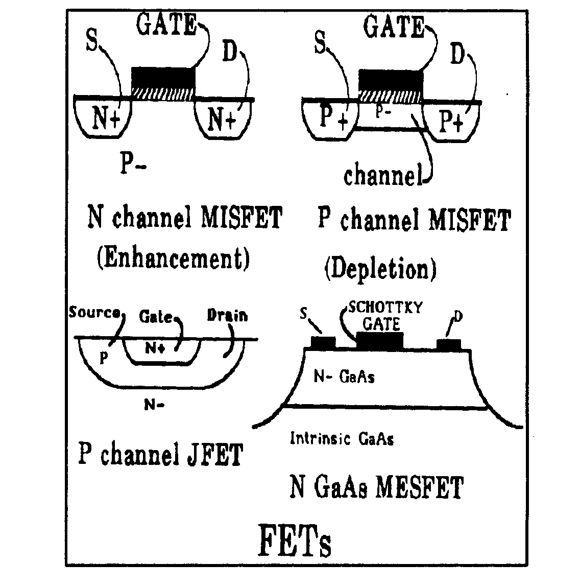
| SEE OR SEARCH CLASS:
| 331, | Oscillators,
subclasses 116 and 117 for field effect transistor oscillator active
elements. |
| 341, | Coded Data Generation or Conversion,
subclass 136 for analog to or from digital conversion devices
with a field effect transistor. |
|
| | |
| 214 | Charge injection device: |
| | This subclass is indented under subclass 213. Subject matter wherein the field effect device is a device
in which storage sites for packets of electric charge are induced
at or below the surface of the active solid-state (semiconductor) device
by an electric field applied to the device and wherein carrier potential
energy per unit charge minima are established at a given storage
site and such charge packets are injected into the device substrate
or into a data bus.
| | (1)
Note. This type device differs from a charge transfer device
in that, in the latter, charge is transferred to adjacent charge
storage sites in a serial manner whereas in the former, the charge
is injected in a non-serial manner to the device substrate or a
data bus. | |
| | |
| 215 | Charge transfer device: |
| | This subclass is indented under subclass 213. Subject matter in which storage sites for packets of electric
charge are induced at or below the surface of the active solid-state
(semiconductor) device by an electric field applied to the device
and wherein carrier potential energy per unit charge minima are
established at a given storage site and such minima are transferred
to one or more adjacent storage sites in a serial manner.
SEE OR SEARCH THIS CLASS, SUBCLASS:
| 183.1, | for heterojunction type charge transfer devices. |
SEE OR SEARCH CLASS:
| 438, | Semiconductor Device Manufacturing: Process,
subclass 60 for methods of making a photo-responsive semiconductor
integrated circuit having a charge transfer device combined with
another electrical device, subclasses 75+ for methods of
making a photoresponsive charge transfer device, and subclasses
144+ for methods of making a charge transfer device. |
|
| | |
| 217 | Having a conductive means in direct contact with channel
(e.g., non-insulated gate): |
| | This subclass is indented under subclass 216. Subject matter wherein an electrical conductor (e.g., electrode)
directly contacts the channel region of the charge transfer device
(e.g., a non-insulated gate (control) electrode).
| | (1)
Note. The conductive means in direct contact with the channel
may be directly connected to the substrate. |
| | (2)
Note. The conductive means in direct contact with the channel
may be made of metal, forming a Schottky contact with the semiconductor
channel material, i.e., a metal-semiconductor junction. | |
| | |
| 219 | Impurity concentration variation: |
| | This subclass is indented under subclass 216. Subject matter wherein the majority signal carrier charge
transfer device contains impurity dopant ions which vary in terms
of concentration in all or part of the channel of the device.
| | (1)
Note. The impurity dopant ion concentration may vary across
the channel and channel substrate interface. | |
| | |
| 220 | Vertically within channel (e.g., profiled): |
| | This subclass is indented under subclass 219. Subject matter wherein the impurity dopant ion concentration
in the channel of the device varies across the channel in a direction
perpendicular to a main surface of the device, regardless of the
orientation of the channel (e.g., parallel or perpendicular to a
main surface of the device). |
| | |
| 224 | Channel confinement: |
| | This subclass is indented under subclass 216. Subject matter wherein the majority carrier charge transfer
device has means to restrict the dimensions of the thin semiconductor
conductive path region (charge transfer channel) between the source
and drain of the device. |
| | |
| 228 | Light responsive, back illuminated: |
| | This subclass is indented under subclass 225. Subject matter wherein the non-electrical input responsive
device has two major opposed surfaces, the channel containing the
charge carrier storage sites being at or below one surface, and wherein
the device is responsive to light which is incident on the other
major surface. |
| | |
| 229 | Having structure to improve output signal (e.g., exposure
control structure): |
| | This subclass is indented under subclass 225. Subject matter wherein the non-electrical input responsive
device contains structural means to improve the electrical signal
it generates in response to the non-electrical input signal.
| | (1)
Note. The structural means to improve the output signal may
control the amount of charge generated by light incident on the
device which is transferred as output signal charge. | |
| | |
| 230 | With blooming suppression structure: |
| | This subclass is indented under subclass 229. Subject matter wherein the structural means to improve the
output signal prevents spill over of a large amount of signal charge
generated at a storage site which receives a non-electrical input
signal of very high intensity to adjacent storage sites.
| | (1)
Note. The antiblooming suppression structure may include
a drain structure for removing charge from storage sites. |
| | (2)
Note. The antiblooming drain structure may be located in
the device beneath storage sites rather than on its surface. | |
| | |
| 231 | 2-dimensional area architecture: |
| | This subclass is indented under subclass 225. Subject matter wherein the device has a plurality of non-electrical
input responsive means spread out over a two dimensional area, e.g.,
a matrix or array of such means.
| | (1)
Note. One 2-dimensional architecture area may be provided
for light imaging elements and a separate 2-dimensional architecture
area may be provided for electrical signal storage elements. |
| | (2)
Note. The imaging element sites may also be charge transfer
storage sites (e.g., frame transfer imaging device). | |
| | |
| 234 | Single strip of sensors (e.g., linear imager): |
| | This subclass is indented under subclass 225. Subject matter wherein the non-electrical input responsive
device is in the form of a line of individual sensors.
| | (1)
Note. The single strip of sensors may be combined with a
structure forming readout registers, i.e., short term storage devices
for accumulating charge packets generated by the sensors and for
transferring charge packets to an amplifier or output device, and
wherein the sensors are placed adjacent to the readout register
structure. |
| | (2)
Note. The device may have plural readout register structures. | |
| | |
| 235 | Electrical input: |
| | This subclass is indented under subclass 215. Subject matter wherein the input to the charge transfer
device to create the charge to be transferred is an electrical signal. |
| | |
| 236 | Signal applied to field effect electrode: |
| | This subclass is indented under subclass 235. Subject matter wherein means is provided to apply an electrical
signal to an electrode which has an electrical potential barrier
between the electrode and the semiconductor material of the device
(e.g., a MOS dielectric or Schottky contact or reverse-biased junction),
as contrasted with an ohmic electrical contact to the semiconductor. |
| | |
| 239 | Signal charge detection type (e.g., floating diffusion
or floating gate non-destructive output): |
| | This subclass is indented under subclass 215. Subject matter wherein means is provided to detect the amount
of charge being transferred in the device.
| | (1)
Note. The charge being transferred may be measured without
destroying the charge, i.e., the charge packet remains intact. |
| | (2)
Note. The charge transfer device may have a region diffused
with impurity ions not electrically connected to ground to detect
the magnitude of charge being transferred in the device and to output
a signal proportional to that sensed charge. This is known as a
floating diffusion output device. One example of such a device
is a floating diffusion amplifier (FDA). |
| | (3)
Note. The charge transfer device may have a control electrode
not electrically connected to ground to detect the magnitude of
charge being transferred in the device and to output a signal proportional
to that sensed charge. This type device is known as a floating
gate output device. One example of such a device is a floating
gate amplifier (FGA). Devices with plural floating gate outputs
include distributed floating gate amplifiers (DFGA). | |
| | |
| 241 | Multiple channels (e.g., converging or diverging or parallel
channels): |
| | This subclass is indented under subclass 215. Subject matter wherein the charge transfer device contains
more than one channel for charge transfer path.
| | (1)
Note. The channels may converge or diverge, i.e., they are
not parallel to each other, but change direction either toward or
away from each other along their length. |
| | (2)
Note. In such devices, the charge transfer path may lie in
two different (e.g., orthogonal) directions. |
| | (3)
Note. The device may include two or more parallel channels
(e.g., serial- parallel-serial) wherein the charge transfer takes
place in different directions, but the device includes charge transfer
paths that are parallel to each other. | |
| | |
| 242 | Vertical charge transfer: |
| | This subclass is indented under subclass 215. Subject matter wherein the charge transfer device is provided
with structure for vertical charge transfer perpendicular to a main
device surface. |
| | |
| 243 | Channel confinement: |
| | This subclass is indented under subclass 215. Subject matter containing means (e.g., pn junctions or dielectric
layers) to restrict the boundaries of the charge transfer path through
the device.
| | (1)
Note. Typical channel confinement means include use of (a)
an electrically insulating medium; (b) a layer of silicon polymer
material (polysilicon) used to reduce electric field interaction
with charge to be transferred via the channel; or (c) an impurity
ion located in the device substrate, i.e., in the material on which
the device is fabricated (e.g., an implanted channel stop). | |
| | |
| 244 | Comprising a groove: |
| | This subclass is indented under subclass 215. Subject matter wherein a surface of the device includes
an elongated indentation.
| | (1)
Note. The location of the groove relative to the charge storage
sites of the device is deliberately not specified in this definition. | |
| | |
| 246 | Phase structure (e.g., doping variations to provide asymmetry
for 2-phase operation; more than four phases or "electrode
per bit"): |
| | This subclass is indented under subclass 245. Subject matter including a plurality of gate regions or
doping variation regions to permit unidirectional charge packet
transfer by symmetrical or unsymmetrically phased electrical control
signals applied to the device gate or gates.
| | (1)
Note. The phase structure may be multiphase (e.g., 3-phase
or 4-phase), i.e., with three sets or four sets of electrodes, respectively. |
| | (2)
Note. Search subclass 249, below, for 2-phase structure devices. |
| | (3)
Note. Means may also be provided to generate a traveling
wave of non-electrical energy (e.g., acoustic energy) in the device. | |
| | |
| 248 | 2-phase: |
| | This subclass is indented under subclass 246. Subject matter wherein the device has two sets of gate electrodes. |
| | |
| 250 | Plural gate levels: |
| | This subclass is indented under subclass 249. Subject matter wherein the electrode structures include
more than one level of gate electrodes relative to a main surface
of the device. |
| | |
| 256 | Junction field effect transistor (unipolar transistor): |
| | This subclass is indented under subclass 213. Subject matter wherein the field effect device is a junction
field effect transistor, i.e., in which current flow through a
thin channel of semiconductor material is controlled by an electric
field applied to a control region or electrode in rectifying contact
(i.e., a pn junction or Schottky barrier junction) with the semiconductor
material of the channel, so that the depletion region extending
into the channel from the rectifying contact reduces the thickness
of the undepleted portion of the channel to reduce the current flow
through the channel.
SEE OR SEARCH CLASS:
| 438, | Semiconductor Device Manufacturing: Process, particularly
subclasses 167+ for methods of forming a Schottky gate field effect
device and subclasses 186+ for methods of forming a junction
gate field effect device. |
|
| | |
| 258 | In imaging array: |
| | This subclass is indented under subclass 257. Subject matter wherein a plurality of light responsive JFETs
or JFETs combined with a light responsive device are in the form
of a one or two dimensional array (e.g., line or area array) for
forming an image of an object, light from which is incident upon
the array. |
| | |
| 259 | Elongated active region acts as transmission line or distributed
active element (e.g., "transmission line" field
effect transistor): |
| | This subclass is indented under subclass 256. Subject matter including at least one elongated active region
(source, gate, or drain) which transmits or distributes charge carriers.
| | (1)
Note. When the impedance of an element at the operating frequency
is due primarily to the parameters of the element itself, and in
considering the inductance, capacitance, and resistance of the element
they must be considered as mixed together and spread out along the element
rather than being considered as separate discrete lumps or components as
in the case of simple series and parallel circuits, the element
may be said to have distributed parameters. |
SEE OR SEARCH CLASS:
| 333, | Wave Transmission Lines and Networks, appropriate subclasses for transmission lines or
distributed elements, per se. |
| 438, | Semiconductor Device Manufacturing: Process, particularly
subclasses 167+ for methods of forming a Schottky gate field effect
device and subclasses 186+ for methods of forming a junction
gate field effect device. |
|
| | |
| 260 | Same channel controlled by both junction and insulated
gate electrodes, or by both Schottky barrier and pn junction gates
(e.g., "taper isolated" memory cell): |
| | This subclass is indented under subclass 256. Subject matter including plural gate electrodes or regions,
at least one of which is isolated from the channel by a rectifying
junction and at least another of which is isolated from the channel
by an insulating layer therebetween, or wherein one rectifying junction
may be a metal-to-semiconductor (Schottky) type and the other a
pn junction.
| | (1)
Note. In such devices, the junction gate region may be free
of direct electrical connection (e.g., "taper isolated" memory
cell), i.e., wherein the JFET has at least one gate electrode region
which is isolated from the channel by a rectifying junction and
is not directly provided with an electrical connection or terminal. | |
| | |
| 261 | Junction gate region free of direct electrical connection
(e.g., floating junction gate memory cell structure): |
| | This subclass is indented under subclass 256. Subject matter including at least one gate electrode region
which is isolated from the channel by a rectifying junction and
is not directly provided with an electrical connection or terminal.
| | (1)
Note. This type of gate is a floating junction gate, as contrasted
with a floating insulated gate. |
| | (2)
Note. See this class, subclass 315, for floating insulated
gate field effect devices. |
| | (3)
Note. The floating gate region may capacitively store electrical
charge and be used as a memory element. | |
| | |
| 262 | Combined with insulated gate field effect transistor (IGFET): |
| | This subclass is indented under subclass 256. Subject matter including a field effect transistor having
a gate (control) electrode which is electrically insulated from
the channel and other electrodes of the transistor.
| | (1)
Note. The combined JFET and IGFET may be electrically connected
so that the source or drain electrode of one FET is connected to
the gate electrode of the other FET. | |
| | |
| 263 | Vertical controlled current path: |
| | This subclass is indented under subclass 256. Subject matter wherein the operating current of the JFET
has a path perpendicular to a main surface of the JFET and is controlled
by the gate electrode of the device. |
| | |
| 264 | Enhancement mode or with high resistivity channel (e.g.,
doping of 1015cm-3 or
less): |
| | This subclass is indented under subclass 263. Subject matter wherein an increase in the magnitude of the
gate bias voltage increases the operating current, only leakage
current flows when the gate voltage is zero, and conduction does
not begin until the gate voltage reaches a threshold value; or the
JFET has a channel made of relatively high electrical resistivity, e.g.,
due to doping with impurity ions of 1015 cm-3or
less. |
| | |
| 268 | Enhancement mode: |
| | This subclass is indented under subclass 256. Subject matter wherein an increase in the magnitude of the
gate bias voltage increases the operating current, only leakage
current flows when the gate voltage is zero, and conduction does
not begin until the gate voltage reaches a threshold value. |
| | |
| 273 | With bipolar device: |
| | This subclass is indented under subclass 272. Subject matter located in an integrated circuit with a device
which operates using both positive and negative charge carriers.
| | (1)
Note. An active solid-state electronic device that contains
both bipolar and field effect transistors may be referred to as
a BI-FET device. | |
| | |
| 280 | With Schottky gate: |
| | This subclass is indented under subclass 256. Subject matter including a metal to semiconductor rectifying
(i.e., Schottky barrier) gate electrode.
| | (1)
Note. A Schottky barrier gate JFET is referred to commonly
as a MESFET (MEtal-Semiconductor field effect
transistor). | |
| | |
| 286 | With non-uniform channel thickness or width: |
| | This subclass is indented under subclass 256. Subject matter wherein the channel has a non-uniform width
or thickness (which lies in a plane perpendicular to both the channel
length and width).
| | (1)
Note. Channel length is measured along a line connecting
the source and drain, while channel width is measured perpendicular
to the length. Both length and width lie in a plane, parallel to
the device surface. See the illustration, below.
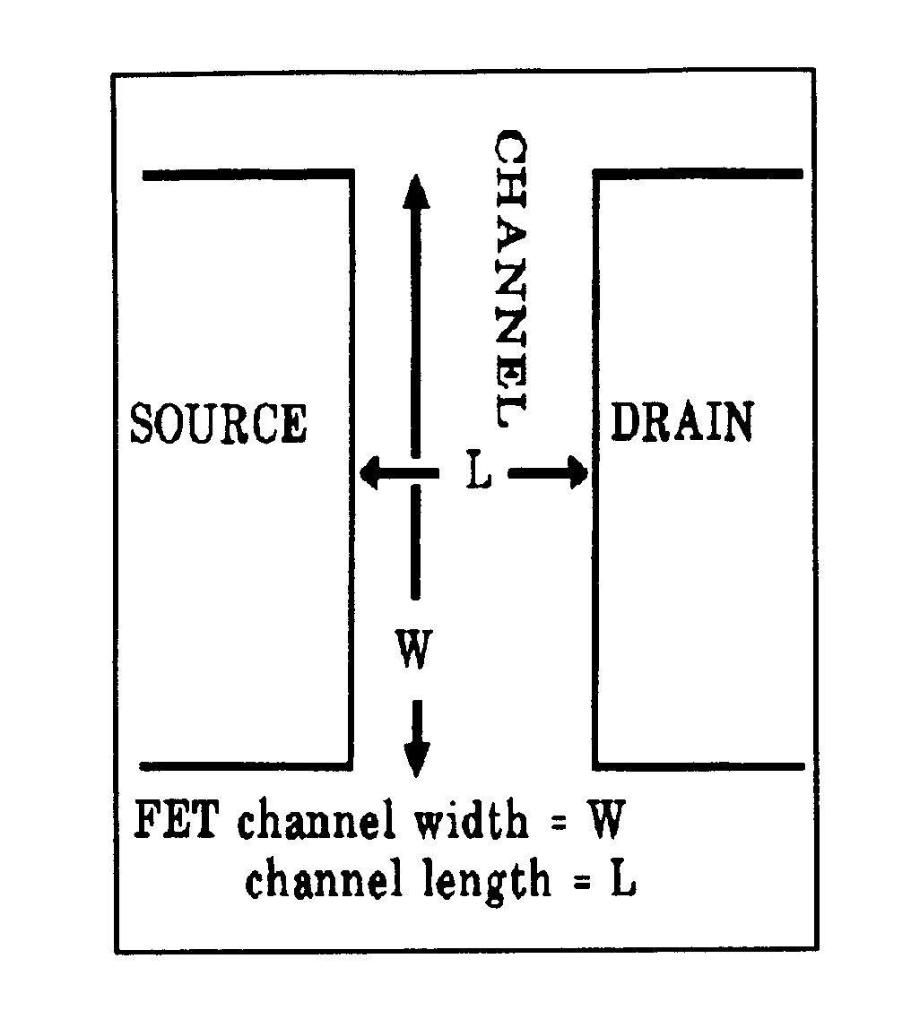
| |
| | |
| 288 | Having insulated electrode (e.g., MOSFET, MOS diode): |
| | This subclass is indented under subclass 213. Subject matter including an electrode which is electrically
insulated from the active semiconductor region of the device (e.g.,
a metal oxide semiconductor insulated electrode).
| | (1)
Note. Typically the insulated electrode is the control or
gate electrode. |
SEE OR SEARCH CLASS:
| 438, | Semiconductor Device Manufacturing: Process, particularly
subclasses 197+ for methods of forming an insulated gate field
effect device. |
|
| | |
| 291 | Imaging array: |
| | This subclass is indented under subclass 290. Subject matter comprising a one or more dimensional array
of light responsive devices which generate an electronic image of
light from an object incident thereupon. |
| | |
| 294 | With shield, filter, or lens: |
| | This subclass is indented under subclass 291. Subject matter including means to shield the array from
unwanted light, to filter light incident on the array, or to refract
light incident on the array (e.g., to focus an image of an object on
the array). |
| | |
| 296 | Insulated gate capacitor or insulated gate transistor combined
with capacitor (e.g., dynamic memory cell): |
| | This subclass is indented under subclass 288. Subject matter wherein the device gate acts as a capacitor
(i.e., wherein a positive potential placed on the gate electrode
creates a negative charge on the other side of the insulator in
the semiconductor material of the device, and vice versa) or the
device is a transistor and it is combined with a capacitor.
SEE OR SEARCH CLASS:
| 438, | Semiconductor Device Manufacturing: Process, particularly
subclasses 239+ for methods of forming an insulated gate field
effect transistor combined with a capacitor and subclasses 386 through
399 for manufacture of a capacitors, per se, utilizing a semiconductor
substrate. |
|
| | |
| 297 | With means for preventing charge leakage due to minority
carrier generation (e.g., alpha generated soft error protection
or "dark current" leakage protection): |
| | This subclass is indented under subclass 296. Subject matter wherein the device further includes means
(1) to prevent electrical charge in the capacitor or capacitive
type insulated gate region of the transistor to leak therefrom, or
(2) to prevent excess leakage currents across pn junctions due
to generation of minority carriers in the device for example (a)
alpha particles incident on the device or (b) thermal generation
of electron-hole pairs, or (c) minority carriers injected into
the semiconductor substrate by other devices in the same substrate.
| | (1)
Note. Junctions across which excess leakage is sought to
be prevented typically include (a) the source or drain junction
of an insulated gate field effect transistor or (b) a connecting
BIT line of a memory array which is isolated by a pn junction from
a semiconductor substrate. | |
| | |
| 302 | Vertical transistor: |
| | This subclass is indented under subclass 301. Subject matter combined with a vertical transistor (i.e.,
one in which the operating current flow is perpendicular to a main
surface of the device). |
| | |
| 303 | Stacked capacitor: |
| | This subclass is indented under subclass 301. Subject matter wherein the trench capacitor device contains
a number of capacitor electrode regions stacked vertically above
each other or wherein the capacitor and the transistor are located
such that one overlies the other. |
| | |
| 306 | Stacked capacitor: |
| | This subclass is indented under subclass 296. Subject matter wherein the capacitor device contains a number
of capacitor electrode regions overlying each other or where the capacitor
and the transistor are located such that one overlies the other. |
| | |
| 313 | Inversion layer capacitor: |
| | This subclass is indented under subclass 296. Subject matter wherein one plate of the capacitor device
is a layer of minority carriers opposite in conductivity type to
the doping of the semiconductor which are induced by applied voltage. |
| | |
| 314 | Variable threshold (e.g., floating gate memory device): |
| | This subclass is indented under subclass 288. Subject matter wherein the device has a threshold voltage
for current conduction which may be varied (e.g., by storage of
charge in an insulator layer adjacent the channel in response to an
electrical "write" signal).
SEE OR SEARCH THIS CLASS, SUBCLASS:
| 239, | for a floating gate signal charge detection type
charge transfer device. |
| 261, | for a floating gate JFET. |
SEE OR SEARCH CLASS:
| 365, | Static Information Storage and Retrieval, appropriate subclass for read/write static storage
systems, and
subclasses 185.01+ for predominate structure of floating gate memory storage
(e.g., flash memory), particularly subclass 185.24 for threshold setting
(e.g., conditioning). |
|
| | |
| 315 | With floating gate electrode: |
| | This subclass is indented under subclass 314. Subject matter including a gate electrode which is free
of direct electrical connection.
SEE OR SEARCH CLASS:
| 365, | Static Information Storage and Retrieval, appropriate subclass for read/write static storage
systems, and
subclasses 185.01+ for predominate structure of floating gate memory storage
(e.g., flash memory), particularly subclass 185.24 for threshold setting
(e.g., conditioning). |
|
| | |
| 323 | With means to facilitate light erasure: |
| | This subclass is indented under subclass 315. Subject matter including means to make erasure of the electrical
charge content of the device by light easier (e.g., by providing
an ultraviolet light window layer over the floating gate electrode
to reduce absorption of erasing light). |
| | |
| 327 | Short channel insulated gate field effect transistor: |
| | This subclass is indented under subclass 288. Subject matter wherein the field effect device is an insulated
gate field effect transistor with a short channel (i.e., one wherein
the length of the channel is sufficiently short that the threshold
voltage of the transistor depends on the length of the channel,
or where the channel is specified to be less than 2 micrometers
in length). |
| | |
| 329 | Gate controls vertical charge flow portion of channel (e.g.,
VMOS device): |
| | This subclass is indented under subclass 327. Subject matter wherein the short channel IGFET has a channel
portion in which charge flows in a substantially vertical direction
and wherein the charge flowing therein is controlled by the gate
electrode.
| | (1)
Note. An IGFET"s short channel may have horizontal
as well as vertical charge flow portions. This subclass provides for
those devices in which the vertical charge flow portion, i.e., the
portion of the channel in which charge is flowing substantially
in a vertical direction, of the channel is controlled by the gate. | |
| | |
| 330 | Gate electrode in groove: |
| | This subclass is indented under subclass 329. Subject matter wherein the gate controlled vertical channel
device has a groove located therein and a gate electrode located
in the groove. |
| | |
| 337 | In integrated circuit structure: |
| | This subclass is indented under subclass 335. Subject matter wherein the graded channel doping short channel
IGFET is contained in a single monolithic chip with other active
or passive solid-state electronic devices. |
| | |
| 338 | With complementary field effect transistor: |
| | This subclass is indented under subclass 337. Subject matter wherein the graded channel doping short channel
IGFET is contained in a single monolithic chip with a field effect
transistor with a polarity type opposite to that of the graded channel
doping short channel IGFET. |
| | |
| 339 | With means to increase breakdown voltage: |
| | This subclass is indented under subclass 335. Subject matter wherein the graded channel doping short channel
IGFET includes means to increase the voltage that may be applied
to the device without electrical breakdown of the device occurring. |
| | |
| 347 | Single crystal semiconductor layer on insulating substrate
(SOI): |
| | This subclass is indented under subclass 288. Subject matter wherein the field effect device has a single
crystal semiconductor layer located on a substrate made of electrically
insulating material.
| | (1)
Note. See this class, subclass 49, for active solid-state
devices in non-single crystalline layers which may be on insulating
substrates. See this class, subclass 506, for active devices in
single crystal layers which are dielectrically isolated, but do
not include field effect devices. |
| | (2)
Note. Material deposited as polycrystalline or amorphous
and then recrystallized, as by a scanning laser beam, is considered
to be non-single crystalline for purposes of determining classification
between this subclass and subclass 49, since such recrystallization
typically leaves residual grain boundaries and is thus large grained
polycrystalline material, rather than true single crystal material. |
SEE OR SEARCH CLASS:
| 438, | Semiconductor Device Manufacturing: Process, particularly
subclasses 149+ for methods of forming a field effect transistor
on an insulating substrate or layer (e.g., SOS, SOI, etc.). |
|
| | |
| 348 | Depletion mode field effect transistor: |
| | This subclass is indented under subclass 347. Subject matter wherein the SOI device is a field effect
transistor which operates in the depletion mode, i.e., a FET which
passes maximum operating current with the gate to source biased
to zero volts. |
| | |
| 361 | For operation as bipolar or punchthrough element: |
| | This subclass is indented under subclass 360. Subject matter wherein the insulated gate transistor structure
protection device is configured to operate as a bipolar transistor
or to conduct by punchthrough of a depletion region from one pn
junction to another pn junction upon application of an overvoltage. |
| | |
| 362 | Punchthrough or bipolar element: |
| | This subclass is indented under subclass 356. Subject matter wherein the means for protecting against
insulator breakdown is a bipolar device or is configured to conduct
by punchthrough of a depletion region from one pn junction to another
pn junction upon application of an overvoltage. |
| | |
| 370 | Combined with bipolar transistor: |
| | This subclass is indented under subclass 369. Subject matter including at least one bipolar transistor.
| | (1)
Note. An active solid-state electronic device that contains
both bipolar and field effect transistors may be referred to as
a BI-FET device. | |
| | |
| 372 | With means to prevent latchup or parasitic conduction channels: |
| | This subclass is indented under subclass 369. Subject matter including means to prevent conduction between
regions of complementary IGFETs which form a (parasitic) regenerative structure
which remains ON in the absence of a triggering signal.
| | (1)
Note. For a definition of the regenerative structure of this
subclass type, see subclass 107. | |
| | |
| 378 | Combined with bipolar transistor: |
| | This subclass is indented under subclass 368. Subject matter wherein the IGFET is combined with a bipolar
transistor in a single semiconductor chip.
| | (1)
Note. An active solid-state electronic device that contains
both bipolar and field effect transistors may be referred to as
a BI-FET device. | |
| | |
| 382 | With contact to source or drain region of refractory material
(e.g., polysilicon, tungsten, or silicide): |
| | This subclass is indented under subclass 368. Subject matter wherein the device has an electrical contact
to its source region or drain region wherein the contact is made
of a refractory or platinum group metal, or of other material which
has a melting point above that of the iron group of metals and which
is resistant to heat (e.g., of polysilicon, tungsten or silicide).
| | (1)
Note. Refractory materials include refractory metals and
platinum group metals which include metals found in groups IVA,
VA, VIA, or VIIIA (other than iron (Fe), nickel (Ni) or cobalt (Co)) of
the periodic table of the elements. | |
| | |
| 395 | Thick insulator portion: |
| | This subclass is indented under subclass 394. Subject matter wherein the means to prevent parasitic conduction
channels from forming includes a thick insulator portion. |
| | |
| 397 | In vertical-walled groove: |
| | This subclass is indented under subclass 396. Subject matter wherein the recessed thick isolator portion
is in a groove in the surface of the overall device which extends
perpendicular to the surface of the overall device. |
| | |
| 414 | RESPONSIVE TO NON-ELECTRICAL SIGNAL (E.G., CHEMICAL, STRESS, LIGHT,
OR MAGNETIC FIELD SENSORS): |
| | This subclass is indented under the class definition. Subject matter wherein the device generates an electrical
signal in response to a non-electrical signal (e.g., light, heat,
pressure) incident thereon. |
| | |
| 415 | Physical deformation: |
| | This subclass is indented under subclass 414. Subject matter wherein the non-electrical signal incident
upon the active solid-state device is a force which physically deforms
the device.
SEE OR SEARCH CLASS:
| 438, | Semiconductor Device Manufacturing: Process, particularly
subclasses 50+ for methods of forming semiconductor devices which
are responsive to physical deformation. |
|
| | |
| 416 | Acoustic wave: |
| | This subclass is indented under subclass 415. Subject matter wherein the physically deforming force is
in the form of a traveling vibration made up of sound energy.
SEE OR SEARCH THIS CLASS, SUBCLASS:
| 254, | for field effect acoustic wave responsive devices. |
|
| | |
| 417 | Strain sensors: |
| | This subclass is indented under subclass 415. Subject matter wherein the physically deforming force is
that of an applied stress.
SEE OR SEARCH THIS CLASS, SUBCLASS:
| 254, | for field effect strain sensor devices. |
|
| | |
| 421 | Magnetic field: |
| | This subclass is indented under subclass 414. Subject matter wherein the non-electrical signal to which
the active solid-state device responds, is a magnetic field.
SEE OR SEARCH THIS CLASS, SUBCLASS:
| 108, | for regenerative type magnetic field responsive
devices |
|
| | |
| 428 | Electromagnetic or particle radiation: |
| | This subclass is indented under subclass 414. Subject matter wherein the electrical signal is generated
by the device in response to radiant energy in the electromagnetic
energy spectrum or in the form of neutral or charged particles (e.g.,
alpha or beta particles). |
| | |
| 431 | Light: |
| | This subclass is indented under subclass 428. Subject matter wherein the non-electrical signal to which
the device responds is electromagnetic energy in the light frequency/wavelength range
(i.e., from infrared (except where the response is mainly due to
thermal heating due to the infrared radiation) to visible and ultraviolet).
SEE OR SEARCH THIS CLASS, SUBCLASS:
| 21, | for light responsive superlattice quantum well heterojunction
tunneling devices. |
| 53, | through 56, for amorphous semiconductor junction
material devices which are responsive to non-electrical (e.g., light)
signals. |
| 80, | through 85, for light emitters combined with or
also constituting a light responsive device. |
| 113, | through 118, for light activated regenerative type
devices. |
| 184, | through 189, for light responsive heterojunction
devices in non-charge transfer devices. |
| 225, | through 234, for charge transfer devices with non-electrical
(e.g., light) input. |
| 257, | through 258, for light responsive JFET devices. |
| 290, | through 294, for light responsive insulated electrode
field effect devices. |
SEE OR SEARCH CLASS:
| 438, | Semiconductor Device Manufacturing: Process, particularly
subclasses 54+ for methods of making a temperature responsive
semiconductor device. |
|
| | |
| 432 | With optical element: |
| | This subclass is indented under subclass 431. Subject matter wherein the light incident upon the active
region passes through an optical element (e.g., a fiber, lens, filter,
etc.). |
| | |
| 434 | With window means: |
| | This subclass is indented under subclass 433. Subject matter with means to optically couple the light
to the device through a transparent window. |
| | |
| 435 | With optical shield or mask means: |
| | This subclass is indented under subclass 431. Subject matter with means to spatially or temporally block
all or part of the light incident on the portions of the device
receptor region, other than the intended region. |
| | |
| 437 | Antireflection coating: |
| | This subclass is indented under subclass 436. Subject matter wherein the means for increasing light absorption
by the junction is a coating applied to the device which reduces
reflection of the incident light (e.g., by use of interference films). |
| | |
| 438 | Avalanche junction: |
| | This subclass is indented under subclass 431. Subject matter wherein the device has a junction which is
operated in the avalanche portion of its operating curve to utilize
the avalanche multiplication of photocurrent by means of hole-electron
pairs created by absorbed photons.
| | (1)
Note. When the reverse bias voltage applied to the device
approaches breakdown level, the holes or electrons collide with
substrate atoms to produce an avalanche of hole-electron pairs. | |
| | |
| 445 | With antiblooming means: |
| | This subclass is indented under subclass 443. Subject matter with means to prevent more than one individual
light responsive element from being activated by a very bright spot
of light incident on a point of the matrix or array.
| | (1)
Note. The anti-blooming means may drain charge from adjacent
individual array elements to some other area, e.g., the substrate.
This is known as an overflow drain. | |
| | |
| 455 | Silicide of Platinum group metal: |
| | This subclass is indented under subclass 454. Subject matter wherein the Schottky layer is a silicide
of a metal found in the period table listed as a platinum group
metal (i.e., ruthenium, rhodium, palladium, osmium, iridium, and
platinum). |
| | |
| 461 | Light responsive pn junction: |
| | This subclass is indented under subclass 431. Subject matter wherein the device has a junction between
p-type and n-type material which responds to light incident upon
it by generating a signal proportional thereto. |
| | |
| 462 | Phototransistor: |
| | This subclass is indented under subclass 461. Subject matter wherein the pn junction device is a transistor
wherein the device generates an electrical signal in response to
light incident on the transistor. |
| | |
| 467 | Temperature: |
| | This subclass is indented under subclass 414. Subject matter wherein the non-electrical signal to which
the device responds is thermal energy.
| | (1)
Note. Infrared energy incident on the active junction which
does not cause significant thermal heating of the device is classified
in subclass 431. |
SEE OR SEARCH CLASS:
| 438, | Semiconductor Device Manufacturing: Process, particularly
subclasses 54+ for methods of making a temperature responsive
semiconductor device. |
|
| | |
| 470 | Pn junction adapted as temperature sensor: |
| | This subclass is indented under subclass 467. Subject matter wherein the active junction is a pn junction
(i.e., forms a boundary between p-type and n-type carrier materials)
and generates an electrical signal in response to thermal energy
incident upon the active junction. |
| | |
| 471 | SCHOTTKY BARRIER: |
| | This subclass is indented under the class definition. Subject matter wherein the device contains a Schottky barrier
(i.e., a rectifying interface between a semiconductor material and
a metal).
SEE OR SEARCH THIS CLASS, SUBCLASS:
| 54, | for Schottky barrier to amorphous semiconductor
material device. |
| 73, | for Schottky barrier to polycrystalline semiconductor
material device. |
| 155, | for a regenerative type switching device with switching
speed enhancement means (e.g., a Schottky contact). |
| 260, | for JFET having the same channel controlled by,
for example, Schottky barrier and PN junction gates. |
| 280, | through 284, for JFETs with a Schottky gate electrode. |
| 449, | through 457, for a light responsive device with
a Schottky barrier. |
| 928, | for a shorted pn or Schottky junction device. |
SEE OR SEARCH CLASS:
| 438, | Semiconductor Device Manufacturing: Process, particularly
subclasses 570+ for methods of forming a rectifying (Schottky)
contact to a semiconductor. |
|
| | |
| 475 | With doping profile to adjust barrier height: |
| | This subclass is indented under subclass 471. Subject matter wherein the difference in electrical potential
from one side of an active junction to the other has been adjusted
by a distribution of impurity dopant in the semiconductor adjacent
the Schottky junction. |
| | |
| 477 | With bipolar transistor: |
| | This subclass is indented under subclass 476. Subject matter wherein the Schottky barrier device is located
in a single integrated monolithic semiconductor chip with a bipolar
transistor. |
| | |
| 481 | Avalanche diode (e.g., so-called "Zener" diode
having breakdown voltage greater than 6 volts): |
| | This subclass is indented under subclass 471. Subject matter wherein the Schottky barrier is in a device
designed to operate in avalanche breakdown.
SEE OR SEARCH THIS CLASS, SUBCLASS:
| 199, | for an avalanche diode in a non-charge transfer
device having a heterojunction. |
| 551, | for an avalanche diode used as a voltage reference
element combined with pn junction isolation means in an integrated
circuit. |
| 603, | through 606, for avalanche diodes not classified
above those subclasses in this schedule, i.e., not involving a heterojunction
in a non-charge transfer device, or a Schottky barrier, or one used
as a voltage reference element with pn junction isolation means
in an integrated circuit. |
|
| | |
| 484 | Guard ring: |
| | This subclass is indented under subclass 483. Subject matter wherein the means to prevent edge breakdown
is a guard ring (e.g., a pn junction surrounding the periphery of
the Schottky metal). |
| | |
| 487 | WITH MEANS TO INCREASE BREAKDOWN VOLTAGE THRESHOLD: |
| | This subclass is indented under the class definition. Subject matter wherein the device is provided with means
to increase the voltage that may be applied thereto without causing
electrical breakdown. |
| | |
| 488 | Field relief electrode: |
| | This subclass is indented under subclass 487. Subject matter wherein the means to increase breakdown voltage
comprises an electrode insulated from the semiconductor material
of the active solid-state device, and configured so as to reduce
the electric field strength at a given voltage applied to the device. |
| | |
| 489 | Resistive: |
| | This subclass is indented under subclass 488. Subject matter wherein the field relief electrode is a high
resistance layer adapted to have a current flow therethrough and
a corresponding voltage variation therein. |
| | |
| 490 | Combined with floating pn junction guard region: |
| | This subclass is indented under subclass 488. Subject matter wherein the means for increasing breakdown
voltage includes, in addition to a field relief electrode, a floating
pn junction guard region, i.e., a region free of direct electrical
connection located in the material forming one side of an active
pn, or other rectifying semiconductor junction, which region forms
a pn junction with the material of the one side of the active junction,
the guard region being spaced from the active junction, but sufficiently
close thereto that the reverse bias depletion region from the active
junction can reach the guard junction, whereby the guard junction modifies
the shape of the depletion region from the active junction thus
lowering the electric field intensity at a given applied reverse
voltage across the active junction. |
| | |
| 491 | In integrated circuit: |
| | This subclass is indented under subclass 487. Subject matter wherein the device with means to increase
breakdown voltage is combined in a unitary monolithic semiconductor
chip with other active or passive electronic devices.
| | (1)
Note. The means for increasing breakdown voltage in the integrated
circuit active device may include a floating pn junction guard
region, that is, a region, free of direct electrical connection, located
in the material forming one side of an active pn or other rectifying
semiconductor junction, which region forms a pn junction with the
material of the one side of the active junction, the guard region
being spaced from the active junction but sufficiently close thereto that
the reverse bias depletion region from the active junction can reach
the guard junction, whereby the guard junction modifies the shape
of the depletion region from the active junction thus lowering the
electric field intensity at a given applied reverse voltage across
the active junction. |
| | (2)
Note. The means for increasing the breakdown voltage of the
integrated circuit device may include a semiconductor surface portion
having a physical configuration, such as a bevel or mesa, to reduce
electric field strength at a given applied voltage. Typically,
the physical configuration will be such that the depletion region
from a reverse biased junction in the active device reaches the physically
configured surface and is forced by the shape of the surface to spread
wider at a given applied reverse voltage than it would otherwise,
thus reducing the electric field strength in the depletion layer. | |
| | |
| 492 | With electric field controlling semiconductor layer having
a low enough doping level in relationship to its thickness to be
fully depleted prior to avalanche breakdown (e.g., RESURF devices): |
| | This subclass is indented under subclass 491. Subject matter wherein the means to increase breakdown voltage
of the device includes a layer of semiconductor material having
a sufficiently low doping concentration that it may be fully depleted
by the depletion region of a reverse biased junction of the active
device prior to avalanche breakdown of the active device, so that
upon depletion of the layer of semiconductor material, the effective
width of the depletion layer of the reverse biased junction of the
active device is greatly expanded, thus resulting in smaller increases
in electric field intensity with further increases of reverse voltage.
| | (1)
Note. Devices provided with such a layer are sometimes called "RESURF" (Reduced
SURFace Field) devices. |
| | (2)
Note. In silicon, to be fully depleted without avalanche
breakdown, a layer must typically have an integrated doping density
(the line integral of doping density along a path through the thickness
of the layer) of less than 2x10¹² dopant atoms/cm2.
The critical integrated doping density varies depending on the properties
of the particular semiconductor material. | |
| | |
| 494 | Reverse-biased pn junction guard region: |
| | This subclass is indented under subclass 487. Subject matter wherein the means for increasing breakdown
voltage in the device includes a reverse biased pn junction guard
region, that is, a region located in the material forming one side
of an active pn or other rectifying semiconductor junction, which
region forms a pn junction with the material of the one side of
the active junction, the guard region being adapted to be reverse
biased with respect to the material forming one side of the active
junction, and being spaced from the active junction, but sufficiently
close thereto that the reverse bias depletion region from the active
junction can reach the depletion region from the reverse biased
guard junction, whereby the depletion region of the guard junction
modifies the shape of the depletion region from the active junction thus
lowering the electric field intensity at a given applied reverse
voltage across the active junction. |
| | |
| 495 | Floating pn junction guard region: |
| | This subclass is indented under subclass 487. Subject matter wherein the means for increasing breakdown
voltage in the device includes a floating pn junction guard region,
that is, a region, free of direct electrical connection, located
in the material forming one side of an active pn or other rectifying
semiconductor junction, which region forms a pn junction with the
material of the one side of the active junction, the guard region
being spaced from the active junction, but sufficiently close thereto
that the reverse bias depletion region from the active junction
can reach the guard junction, whereby the guard junction modifies the
shape of the depletion region from the active junction thus lowering
the electric field intensity at a given applied reverse voltage across
the active junction. |
| | |
| 496 | With physical configuration of semiconductor surface to
reduce electric field (e.g., reverse bevels, double bevels, stepped mesas,
etc.): |
| | This subclass is indented under subclass 487. Subject matter wherein the means to increase breakdown voltage
includes a semiconductor surface portion having a physical configuration,
such as a bevel or mesa, to reduce electric field strength at a
given applied voltage. Typically, the physical configuration will
be such that the depletion region from a reverse biased junction
in the active device reaches the physically configured surface and
is forced by the shape of the surface to spread wider at a given applied
reverse voltage than it would otherwise, thus reducing the electric
field strength in the depletion layer. |
| | |
| 497 | PUNCHTHROUGH STRUCTURE DEVICE (E.G., PUNCHTHROUGH TRANSISTOR,
CAMEL BARRIER DIODE): |
| | This subclass is indented under the class definition. Subject matter having at least one active pn, Schottky barrier,
or other rectifying junction which can be reverse biased to produce
a depletion layer, the active junction being spaced from a second
junction by a layer of semiconductor material in which the depletion region
extending from the active junction is produced, the second junction
being one capable of supplying minority carriers to the layer of
semiconductor material upon forward bias of the second junction,
and in which the second junction is located sufficiently close to
the active junction that the depletion region from the active junction
can reach the second junction, thereby forward biasing the second
junction and causing the injection of minority carriers therefrom
which traverse the depletion layer and reach the active junction.
SEE OR SEARCH THIS CLASS, SUBCLASS:
| 361+, | for punchthrough structure elements used to protect
against overvoltage gate insulator breakdown of insulated gate devices. |
|
| | |
| 499 | INTEGRATED CIRCUIT STRUCTURE WITH ELECTRICALLY ISOLATED COMPONENTS: |
| | This subclass is indented under the class definition. Subject matter wherein at least one active solid-state device
is provided in a single, monolithic semiconductor chip along with other
active or passive elements in the chip, and means are provided to
electrically isolate different devices in the monolithic chip from each
other.
SEE OR SEARCH THIS CLASS, SUBCLASS:
| 7, | for intervalley transfer bulk effect devices (e.g.,
Gunn effect devices) in a monolithic integrated circuit. |
| 93, | for plural light emitting devices with electrical
isolation means in integrated circuit structure. |
| 265, | for JFET devices having vertical current path in
integrated circuit. |
| 272, | through 278, for JFET devices in integrated circuits. |
| 334, | for short channel IGFET devices having a gate electrode
controlling the vertical portion of the channel and being in a groove
in an integrated circuit. |
| 337, | and 338, for graded channel short channel IGFET
devices in integrated circuit structure. |
| 357, | through 359, for insulated electrode field effect
devices with gate insulator overvoltage protection means in complementary
field effect transistor integrated circuit devices. |
| 368, | through 401, for IGFET devices in integrated circuit. |
| 427, | for a magnetic field sensor in an integrated circuit. |
| 446, | for matrix or array type photodetectors with specific
isolation means in an integrated circuit. |
| 491, | and 492, for devices with means to increase breakdown
voltage in an integrated circuit, including, for example, RESURF
devices. |
| 663, | for a superconductive contact or lead on an integrated
circuit. |
| 713, | for cooling means for an integrated circuit device. |
| 758, | through 760, for multi-level metallization in, e.g.,
an integrated circuit device. |
| 922, | for a device with means to prevent inspection of
or tampering with an integrated circuit. |
| 929, | for pn junction isolated integrated circuits with
isolation walls having minimum dopant concentration at intermediate
depth in epitaxial layer. |
SEE OR SEARCH CLASS:
| 438, | Semiconductor Device Manufacturing: Process, particularly
subclasses 294+ for methods of making laterally spaced, electrically
isolated semiconductor regions in combination with insulated gate
field effect transistors; subclasses 353+ for methods of
making laterally spaced, electrically isolated semiconductor regions
in combination with bipolar transistors; and subclasses 400+ for
methods of making laterally spaced, electrically isolated semiconductor
regions or various |
|
| | |
| 500 | Including high voltage or high power devices isolated from
low voltage or low power devices in the same integrated circuit: |
| | This subclass is indented under subclass 499. Subject matter wherein the monolithic chip includes both
electronic components specifically configured for operation at high
voltages or high power levels, along with other electronic components
which are configured for operation only at low voltages or power
levels.
| | (1)
Note. See this class, subclass 491 for monolithic chips which
include active components with specific means provided to increase
the breakdown voltage of those active components. The combination
of high voltage and low voltage active solid-state devices on the
same monolithic chip will only be classified in this subclass (500),
if no particular structure is provided to increase the breakdown
voltage of the high voltage components. | |
| | |
| 501 | Including dielectric isolation means: |
| | This subclass is indented under subclass 500. Subject matter wherein the means to electrically isolate
different devices in the same monolithic chip, containing both high
voltage or power and low voltage or power devices, from each other
includes a region of electrical insulator material. |
| | |
| 503 | With contact or metallization configuration to reduce parasitic
coupling (e.g., separate ground pads for different parts of integrated circuit): |
| | This subclass is indented under subclass 499. Subject matter wherein the chip includes contacts or electrical
interconnections, such as metal strips deposited on the surface
of the chip, which contacts or interconnections are configured in
such a manner as to reduce or eliminate unwanted parasitic coupling
of electrical signals from one part or component of the integrated
circuit to another.
| | (1)
Note. Such configuration might be, for example, a shielding
conductive layer connected to fixed potential, or large area metal
pads for connection to external supply voltages with plural separate pads
provided to connect different parts or components of the same integrated circuit
to the same external voltage, to prevent voltage drops from electrical current
flowing between a pad and one component from producing a parasitic varying
voltage applied to another component. |
SEE OR SEARCH THIS CLASS, SUBCLASS:
| 659, | for electrical shielding, in general, in active
solid-state devices. |
| 664, | for transmission line connections, in general, in
active solid-state devices. |
|
| | |
| 505 | With polycrystalline semiconductor isolation region in
direct contact with single crystal active semiconductor material: |
| | This subclass is indented under subclass 499. Subject matter wherein the means for electrically isolating
different devices in the chip from each other includes at least
one region of polycrystalline (i.e., made up of many small crystals)
semiconductor material, which polycrystalline isolation region is
in direct contact with at least one region of single crystal semiconductor
material which forms part of an active solid-state device in the
chip.
| | (1)
Note. The polycrystalline isolation region may be either
undoped or doped with recombination center doping, in order to make
it high resistivity and thus, effectively, an electrical insulator,
or may be doped with a p or n dopant in order to form a pn junction
with the single crystal material of the active solid-state device
so that the rectifying junction between the doped isolation region and
the single crystal active portion, when reverse biased, electrically
isolates the devices in the chip from each other. | |
| | |
| 507 | With single crystal insulating substrate (e.g., sapphire): |
| | This subclass is indented under subclass 506. Subject matter wherein the means to electrically isolate
different devices from each other includes a substrate of single
crystal insulating material, upon which the semiconductor material
of the active devices is grown in heteroepitaxial relationship therewith.
| | (1)
Note. The substrate may typically be the alpha crystalline
phase of aluminum oxide, commonly called sapphire or single crystalline
beryllium oxide or single crystal magnesium aluminate known as spinel. | |
| | |
| 509 | Combined with pn junction isolation (e.g., isoplanar, LOCOS): |
| | This subclass is indented under subclass 506. Subject matter wherein the means for electrically isolating
components in the chip from each other includes, in addition to
portions of electrical insulator material, pn junctions separating
regions of active devices from each other and/or from a
supporting semiconductor substrate.
| | (1)
Note. There are several names in common use for isolation
of this type, particularly where the pn junctions provide isolation
between active devices and the supporting semiconductor substrate
with the dielectric material recessed into the semiconductor between
active devices and extending down to the isolating pn junctions
to separate devices laterally from each other. Such common names include
LOCOS (Local Oxidation of Silicon), ROI (Recessed Oxide Isolation), Isoplanar,
and Planox. These terms do not represent different isolation structures,
but are merely alternative names for the same type of isolation. | |
| | |
| 510 | Dielectric in groove: |
| | This subclass is indented under subclass 509. Subject matter wherein the electrical insulator material
forming part of the isolation means is located in grooves in the
semiconductor surface (e.g., LOCOS)
SEE OR SEARCH THIS CLASS, SUBCLASS:
| 374, | for CMOS FET dielectric isolation means (e.g., dielectric
layer in vertical groove.) |
|
| | |
| 512 | Complementary devices share common active region (e.g.,
integrated injection logic, I2L): |
| | This subclass is indented under subclass 511. Subject matter wherein the device includes structures wherein
a pnp transistor shares a semiconductor region with an npn transistor, e.g.,
where the base region of the pnp transistor serves also as the emitter
of the npn transistor and the collector of the pnp transistor serves
as the base region of the npn transistor.
| | (1)
Note. Search this class, subclass 107 for regenerative switching
devices, which typically are in the form of a pnp transistor and
an npn transistor, the collector and base of the pnp transistor
forming the base and collector, respectively, of the npn transistor. |
| | (2)
Note. A typical structure in which pnp transistors and npn
transistors share regions in common is that called Integrated injection
logic, I2L (formerly alternatively called merged
transistor logic, MTL), in which a pnp transistor serves to supply
base region current to a multicollector npn transistor, with the base
region of the npn being the logic circuit input and the multiple
collectors providing logic fan out to plural further logic gates. | |
| | |
| 513 | Vertical walled groove: |
| | This subclass is indented under subclass 510. Subject matter wherein the dielectric isolation is located
in grooves in the surface of the overall device which extend perpendicular
to the surface of the overall device. |
| | |
| 514 | With active junction abutting groove (e.g., "walled
emitter"): |
| | This subclass is indented under subclass 513. Subject matter wherein at least one pn junction forming
a part of an active solid-state device terminates against the dielectric
filling in the vertical walled isolation groove.
| | (1)
Note. If the emitter-base junction terminates against a dielectric
isolation sidewall, this is termed a "walled emitter" transistor
structure. | |
| | |
| 521 | Sides of grooves along major crystal planes (e.g., (111),
(100) planes, etc.): |
| | This subclass is indented under subclass 510. Subject matter wherein the device has grooves for the isolation
whose sides are oriented along one or more major crystal planes
of the semiconductor material in which the grooves are formed.
| | (1)
Note. Major crystal planes are considered to be the (111),
(110), and (100) planes in a crystal with cubic symmetry. |
| | (2)
Note. See illustration, below.
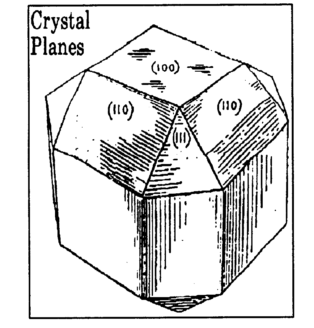
| |
| | |
| 522 | Air isolation (e.g., beam lead supported semiconductor
islands): |
| | This subclass is indented under subclass 506. Subject matter wherein the isolation means is air (e.g.,
islands of semiconductor material supported by beam leads and separated
by air).
SEE OR SEARCH CLASS:
| 438, | Semiconductor Device Manufacturing: Process, particularly
subclass 411 for methods of forming electrically isolated semiconductor
islands held in place by beam lead metallization; subclass 461 for
methods of forming beam leads on a semiconductor substrate combined
with dicing of the substrate into plural separate bodies; and subclass
611 for methods of forming beam lead metallization on a semiconductor
substrate. |
|
| | |
| 528 | Passive components in ICs: |
| | This subclass is indented under subclass 499. Subject matter wherein the device is contained in a single,
monolithic chip with electrical components which are passive, i.e.,
which do not have gain, for example, pure capacitors, inductors,
or resistors.
SEE OR SEARCH THIS CLASS, SUBCLASS:
| 379, | for a passive component combined with an IGFET device
in an integrated circuit. |
| 516, | for passive components in an integrated circuit
with dielectric in groove and pn junction isolation. |
| 904, | for a FET combined with passive components adapted
for use as a static memory cell. |
|
| | |
| 529 | Including programmable passive component (e.g., fuse): |
| | This subclass is indented under subclass 528. Subject matter wherein a passive component is programmable,
i.e., may be permanently altered (e.g., a fuse - a protective device designed
to open a circuit in response to an excessive current).
SEE OR SEARCH CLASS:
| 438, | Semiconductor Device Manufacturing: Process, particularly
subclasses 467 , 600, and 601 for methods of forming or modifying
electrically alterable structures for selectively interconnecting
electrical devices on a semiconductor substrate. |
|
| | |
| 530 | Anti-fuse: |
| | This subclass is indented under subclass 529. Subject matter wherein an element which is normally non-conductive
is made conductive (e.g., a capacitor) that is, that can be selectively electrically
shorted. |
| | |
| 531 | Including inductive element: |
| | This subclass is indented under subclass 528. Subject matter wherein the device includes an electrical
inductor, i.e., an element that tends to oppose any change of current
applied thereto because of a magnetic field generated by the inductor
itself. |
| | |
| 532 | Including capacitor component: |
| | This subclass is indented under subclass 528. Subject matter wherein the device includes an electrical
capacitor, i.e., a passive element with electrical conductors separated
by a dielectric material which stores electrical charge when potential
differences exist between the conductive elements of the capacitor. |
| | |
| 541 | Pinch resistor: |
| | This subclass is indented under subclass 539. Subject matter wherein the resistor element has a structure
in the form of a layer of one conductivity type sandwiched between
a pair of regions of opposite conductivity type, so that the upper
region of opposite conductivity type restricts the thickness of
the resistive layer and thus increases its resistivity.
| | (1)
Note. Typically, the resistor will have the same doping profile
as the base region of the bipolar transistor, while the lower opposite
conductivity type region will have the same doping profile as the
bipolar transistor collector, and the upper, or "pinching" region,
will have the same doping profile as the bipolar transistor emitter. | |
| | |
| 542 | Resistor has same doping as emitter or collector of bipolar
transistor: |
| | This subclass is indented under subclass 539. Subject matter wherein the resistor region has the same
doping concentration and profile (e.g., is formed in the same step
as) either the emitter or the collector region of the bipolar transistor
with which the resistor is combined in the same integrated circuit.
| | (1)
Note. Most resistors in bipolar integrated circuits are
formed with the same doping step as the bipolar transistor base regions.
Resistors that are instead formed at the same doping step as the emitter
or collector, rather than the base, go in this subclass. | |
| | |
| 543 | Lightly doped junction isolated resistor (e.g., ion implanted
resistor): |
| | This subclass is indented under subclass 539. Subject matter wherein the resistive element is of the form
of a lightly doped layer of one conductivity type located in a region
of opposite conductivity type, such that the pn junction between
the resistor region and its containing opposite conductivity type
region serves to isolate the resistor.
| | (1)
Note. A resistor region is considered to be lightly doped
if it is substantially less heavily doped than the base region of
the bipolar transistors in the same integrated circuit, or if it
is has a doping density not greater than 100 times that of the opposite
conductivity type region in which it is contained. |
| | (2)
Note. Such lightly doped resistors are typically formed by
the process of ion implantation, wherein desired dopant atoms are
placed in the semiconductor body by ionizing the dopant material
and accelerating the resulting ions through a carefully controlled
voltage to impinge on the surface of the semiconductor material,
so that the depth of the resulting dopant atoms is determined by
the accelerating voltage and the doping density is determined by
the flux of the ion beam. | |
| | |
| 544 | With pn junction isolation: |
| | This subclass is indented under subclass 499. Subject matter wherein the means for electrically isolating
different devices from each other includes a pn junction located
between the devices to be isolated. |
| | |
| 548 | At least three regions of alternating conductivity types
with dopant concentration gradients decreasing from surface of semiconductor
(e.g., "triple-diffused" integrated circuit): |
| | This subclass is indented under subclass 544. Subject matter including at least three regions of alternating
conductivity type (p or n), with each successive region contained
within the previous region, and each of the regions having a doping
concentration which decreases with distance from the same external
surface of the semiconductor body.
| | (1)
Note. Junction isolated integrated circuits of this type
are typically manufactured by starting with an uniformly doped p-type
semiconductor body to serve as the substrate, then diffusing spaced
n-type regions into the P substrate to form collectors of npn transistors,
and then successively diffusing p-type base and n-type emitters
into the spaced n-type regions. Junction isolated integrated circuits
of this type are simple to manufacture, due to the reduced number
of processing steps involved, but suffer from non-optimum doping concentration
profiles, particularly in the collector regions. | |
| | |
| 551 | Including voltage reference element (e.g., avalanche diode,
so-called "Zener diode" with breakdown voltage
greater than 6 volts or with positive temperature coefficient of breakdown
voltage): |
| | This subclass is indented under subclass 544. Subject matter including a voltage reference element, i.e.,
a device which limits the operating voltage of one or more active
devices in the integrated circuit (e.g., an avalanche diode, so-called "Zener
diode" with breakdown voltage greater than 6 volts, or
with positive temperature coefficient of breakdown voltage).
SEE OR SEARCH THIS CLASS, SUBCLASS:
| 199, | for an avalanche diode in a non-charge transfer
device having a heterojunction. |
| 481, | and 482, for Schottky barrier avalanche diodes. |
| 603, | through 606, for avalanche diodes not classified
above those subclasses in this schedule, i.e., not involving a heterojunction
in a non-charge transfer device or a Schottky barrier, or one used
as a voltage reference element with pn junction isolation means
in an integrated circuit. |
|
| | |
| 552 | With bipolar transistor structure: |
| | This subclass is indented under subclass 544. Subject matter wherein the junction isolation is formed
in an integrated circuit between active devices at least one of
which has a bipolar transistor structure. |
| | |
| 556 | Including lateral bipolar transistor structure: |
| | This subclass is indented under subclass 555. Subject matter wherein at least one of the pnp or npn complementary
bipolar transistors is a lateral structure (i.e., has current flow
between its emitter and collector parallel to a major surface of
the semiconductor chip). |
| | |
| 557 | Lateral bipolar transistor structure: |
| | This subclass is indented under subclass 499. Subject matter wherein the device includes at least one
bipolar transistor which has a lateral structure (i.e., has current
flow between its emitter and collector parallel to a major surface of
the semiconductor chip). |
| | |
| 565 | BIPOLAR TRANSISTOR STRUCTURE: |
| | This subclass is indented under the class definition. Subject matter wherein the active solid-state device comprises
at least one bipolar transistor.
SEE OR SEARCH THIS CLASS, SUBCLASS:
| 47, | for bipolar transistor structure having a metal
contact alloyed to elemental semiconductor type pn junction in a non-regenerative
structure. |
| 511, | for complementary bipolar transistor structure having
dielectric-in-groove isolation and pn junction isolation in an integrated
circuit. |
| 517, | and 518, for bipolar transistor structure having
dielectric-in-groove isolation and pn junction isolation in an integrated
circuit. |
| 525, | for complementary bipolar structure with full dielectric
isolation in an integrated circuit. |
| 526, | for bipolar structure with full dielectric isolation
in an integrated circuit. |
| 552, | through 556, for bipolar transistor structure combined
with pn junction isolation in an integrated circuit. |
| 557, | through 562, for integrated circuits with electrically
isolated lateral bipolar transistor structure. |
SEE OR SEARCH CLASS:
| 148, | Metal Treatment, digests 10 and 11 for bipolar transistor devices. |
| 326, | Electronic Digital Logic Circuitry, particularly
subclasses 18+ , 42+, 48, 75+, 89+,
109+, and 124+ for logic circuits utilizing bipolar
transistors. |
| 327, | Miscellaneous Active Electrical Nonlinear Devices,
Circuits, and Systems, particularly
subclasses 204 , 207, 405, 411+, 417, 432+, 439,
459, 462, 463, 474, 475, and 478+ for miscellaneous nonlinear
circuits with explicitly recited bipolar transistors. |
| 330, | Amplifiers,
subclasses 250+ for amplifiers with transistors which may be bipolar
transistors and subclass 300 which explicitly provides for bipolar or
field effect transistors. |
| 341, | Coded Data Generation or Conversion,
subclasses 127+ for bipolar analog to or from digital converters
and subclass 133 for such device with a drift (graded base) transistor
element. |
| 438, | Semiconductor Device Manufacturing: Process,
subclasses 309+ for methods of forming bipolar transistors. |
|
| | |
| 566 | Plural non-isolated transistor structures in same structure: |
| | This subclass is indented under subclass 565. Subject matter wherein the bipolar structure includes more
than one bipolar transistor in a structure without electrical isolation
between transistors.
| | (1)
Note. See subclass 499, above, for integrated circuits with
electrical isolation, including with bipolar transistors. | |
| | |
| 569 | Complementary Darlington-connected transistors: |
| | This subclass is indented under subclass 567. Subject matter wherein the Darlington configuration comprises
two bipolar transistors which have a complementary connection,
i.e., the input transistor is of one conductivity type (e.g., npn)
and the other is of the opposite conductivity type (e.g., pnp). |
| | |
| 575 | Including lateral bipolar transistor structure: |
| | This subclass is indented under subclass 574. Subject matter wherein at least one of the complementary
bipolar transistors sharing a common region is a lateral bipolar
transistor (i.e., has current flow between its emitter and collector
parallel to a major surface of the semiconductor chip).
SEE OR SEARCH THIS CLASS, SUBCLASS:
| 423, | for lateral and other bipolar transistor magnetic
field responsive structure. |
| 557+, | for electrically isolated lateral bipolar transistor
structures in an integrated circuit. |
|
| | |
| 589 | Avalanche transistor: |
| | This subclass is indented under subclass 565. Subject matter wherein the device is a bipolar transistor
designed to be operated with its base-collector junction biased
into avalanche breakdown. |
| | |
| 594 | WITH GROOVE TO DEFINE PLURAL DIODES: |
| | This subclass is indented under the class definition. Subject matter wherein the active solid-state device has
more than one diode and has a groove therein to separate the diodes. |
| | |
| 595 | VOLTAGE VARIABLE CAPACITANCE DEVICE: |
| | This subclass is indented under the class definition. Subject matter wherein the active solid-state device has
a capacitance which varies with the voltage applied thereto.
| | (1)
Note. This type of voltage variable capacitor device is to
be distinguished from voltage variable capacitors (also referred
to as varactors) which are passive devices only and which may be found,
for example, in Class 361, Electricity: Electrical Systems and
Devices, subclass 277, and Class 332, Modulators, subclass 136,
modulators with varactors. |
SEE OR SEARCH THIS CLASS, SUBCLASS:
| 312, | for insulated gate type voltage variable capacitor
devices or voltage variable capacitor devices combined with an insulated
gate transistor. |
| 438, | Semiconductor Device Manufacturing: Process, subclass
379 for methods of forming a voltage variable capacitance device
utilizing a semiconductor substrate. |
| 480, | for a voltage variable capacitor diode with a Schottky
barrier. |
|
| | |
| 603 | AVALANCHE DIODE (E.G., SO-CALLED "ZENER" DIODE
HAVING BREAKDOWN VOLTAGE GREATER THAN 6 VOLTS): |
| | This subclass is indented under the class definition. Subject matter configured to operate in a manner in which
an external voltage is applied in the reverse-conducting direction
of the device junction with sufficient magnitude to cause the potential
barrier at the junction to breakdown due to electrons or holes gaining sufficient
speed to dislodge valence electrons and thus create more hole-electron
current carriers by an avalanche process.
| | (1)
Note. This includes the so-called "Zener" diode
using silicon as a semiconductor which has a breakdown voltage greater
than 6 volts. True Zener diodes conduct by reverse tunneling, and are
classified in subclass 106. However, many avalanche breakdown diodes which
are classifiable in subclass 603 are called "Zener" diodes
even though the breakdown mechanism is avalanche multiplication,
rather than tunneling. In silicon, pn junctions which break down at
less than 5 volts, do so by reverse tunneling, while those that
break down at above 6 volts, do so by avalanche multiplication. |
| | (2)
Note. See the illustration, below:
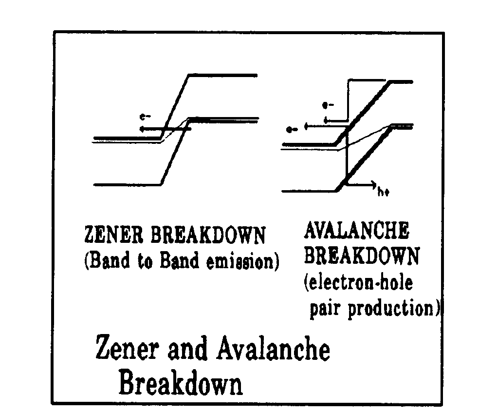
| SEE OR SEARCH THIS CLASS, SUBCLASS:
| 106, | for a reverse bias tunneling diode (Zener diode). |
| 199, | for an avalanche diode having a heterojunction. |
| 481, | for a Schottky barrier avalanche diode. |
| 551, | for an avalanche diode used as a voltage reference
element combined with pn junction isolation means in an integrated
circuit. |
SEE OR SEARCH CLASS:
| 327, | Miscellaneous Active Electrical Nonlinear Devices,
Circuits, and Systems,
subclasses 185+ for stable state circuits which may include an
avalanche diode; subclass 326 for limiting, clipping, or clamping
utilizing an avalanche diode; subclass 502 for gating circuits utilizing
an avalanche diode; and subclass 584 for miscellaneous circuits
utilizing an avalanche diode. |
| 438, | Semiconductor Device Manufacturing: Process,
subclass 91 for methods of making a light responsive avalanche
diode and subclass 380 for making an avalanche diode utilizing a semiconductor
substrate. |
|
| | |
| 604 | Microwave transit time device (e.g., IMPATT diode): |
| | This subclass is indented under subclass 603. Subject matter wherein the device is structured to operate
as a transit time device at microwave frequencies, the frequency
at which it operates being determined by the transit time of charge carriers
through the depletion region which extends on both sides of the
reverse biased junction (e.g., an Impact
ionization avalanche transit time
(IMPATT) diode). |
| | |
| 607 | WITH SPECIFIED DOPANT (e.g., plural dopants of same conductivity
in same region): |
| | This subclass is indented under the class definition. Subject matter wherein the active solid-state device contains
impurity dopant atoms which are specified and are used to change
the conductive properties of the semiconductor material.
| | (1)
Note. If the dopant is in Si or Ge, it may be a shallow level
dopant, other than an element from group III or group V of the periodic
table (e.g., a dopant such as Li in Ge). | |
| | |
| 610 | Deep level dopant: |
| | This subclass is indented under subclass 607. Subject matter including a specified dopant which establishes
traps in the forbidden band of a semiconductor into which carriers
may drop or rise. |
| | |
| 613 | INCLUDING SEMICONDUCTOR MATERIAL OTHER THAN SILICON OR
GALLIUM ARSENIDE (GaAs) (E.G., PbxSn1-xTe): |
| | Subject matter under the subclass definition which includes
semiconducting material other than silicon or gallium arsenide (GaAs). |
| | |
| 617 | INCLUDING REGION CONTAINING CRYSTAL DAMAGE: |
| | This subclass is indented under the class definition. Subject matter wherein the device includes a region which
has crystal damage.
| | (1)
Note. The crystal damage may have been caused by charged
or elementary particles bombardment of a particular region. | |
| | |
| 618 | PHYSICAL CONFIGURATION OF SEMICONDUCTOR (E.G., MESA, BEVEL, GROOVE,
ETC.): |
| | This subclass is indented under the class definition. Subject matter wherein the device has a particular physical
form, such as a mesa or bevel or groove.
SEE OR SEARCH THIS CLASS, SUBCLASS:
| 171, | for regenerative devices with edge features (e.g.,
bevels). |
| 496, | for devices with physical configuration (e.g., bevels)
to increase breakdown voltage threshold. |
| 586, | for bipolar transistor devices with non-planar semiconductor
surfaces (e.g., bevels). |
|
| | |
| 622 | Groove: |
| | This subclass is indented under subclass 618. Subject matter in which there is a physical groove in a
surface of the semiconductor device.
SEE OR SEARCH THIS CLASS, SUBCLASS:
| 117, | and 118, for light activated regenerative type devices
having a groove, e.g., that contains a light conductor. |
| 127, | for a bidirectional rectifier with control electrode
and a groove or guard ring to separate the device into sections
having different conductive polarity. |
| 170, | for a regenerative type device with a groove or
other surface feature to increase breakdown voltage. |
| 244, | for a charge transfer device having a groove. |
| 283, | for a JFET with Schottky gate closely aligned with
source region with a groove or overhang for alignment. |
| 284, | for a JFET with Schottky gate in a groove. |
| 330, | through 334, for a short channel IGFET with a gate
electrode in a groove for controlling a vertical portion of the
device channel. |
| 397, | for an IGFET in an integrated circuit with a thick
insulator portion recessed in a vertical walled groove in the semiconductor
surface to prevent parasitic conduction channels. |
| 466, | for a light responsive device with a physical configuration
feature (e.g., a groove). |
| 534, | for a passive component located in a groove in an
integrated circuit device. |
| 571, | for Darlington configuration bipolar transistor
structure having a nonplanar structure (e.g., a groove). |
| 586, | for a bipolar transistor structure with a nonplanar
surface (e.g., a groove). |
| 589, | for a voltage variable capacitance device with means
to increase active junction area (e.g., a groove). |
|
| | |
| 629 | WITH MEANS TO CONTROL SURFACE EFFECTS: |
| | This subclass is indented under the class definition. Subject matter wherein the active junction device has means
to modify (e.g., reduce, or eliminate) electrical field effects
which take place at the device surface or to modify (e.g., reduce
or eliminate) inhomogeneities in electrical properties of a semiconductor
crystal region due to effects caused by the discontinuity of the crystal
lattice at the surface.
| | (1)
Note. Such effects include formation of an inversion layer
of minority carriers at the semiconductor surface, or depletion of
majority carriers at the semiconductor surface, due to charge in
an insulating coating on the surface or due to dangling bonds where
the crystal structure of the semiconductor ends at the surface,
leakage current via charge flow over a surface rather than through
it, etc. |
SEE OR SEARCH THIS CLASS, SUBCLASS:
| 487, | for a semiconductor device provided with means to
increase breakdown voltage of the device (which may involve surface
effects). |
|
| | |
| 630 | With inversion-preventing shield electrode: |
| | This subclass is indented under subclass 629. Subject matter wherein the means to control surface effects
includes an electrode, insulated from the semiconductor surface,
which electrode is configured to prevent inversion of the conductivity
type of the surface due to surface effects. |
| | |
| 632 | Insulating coating: |
| | This subclass is indented under subclass 629. Subject matter wherein there is a surface coating of electrically
insulating material on the semiconductor body to control surface
effects. |
| | |
| 633 | With thermal expansion compensation (e.g., thermal expansion
of glass passivant matched to that of semiconductor): |
| | This subclass is indented under subclass 632. Subject matter wherein the insulating coating includes means
to compensate for mismatches in thermal expansion coefficient between
different portions of the device, such as forming the insulating
coating of a material which closely matches the thermal expansion
coefficient of the underlying semiconductor.
| | (1)
Note. Typical semiconductor materials, such as silicon, have
extremely low thermal expansion coefficients, and thus, low thermal
expansion materials such as Corning Code 7740 PYREX® borosilicate
glass closely match the expansion coefficient of the semiconductor,
and help to prevent thermal expansion induced stress or cracking. | |
| | |
| 634 | Insulating coating of glass composition containing component
to adjust melting or softening temperature (e.g., low melting point glass): |
| | This subclass is indented under subclass 632. Subject matter wherein the insulating coating comprises
a glass composition containing a component to adjust the melting
or softening temperature.
| | (1)
Note. A commonly used additive to lower the melting point
of silica (silicon dioxide) is phosphorous oxide, producing phosphosilicate
glass. |
| | (2)
Note. Such layers are typically provided so that the device
can be heated to the softening point of the glass to cause it to flow
and smooth out sharp edges on the semiconductor surface that might adversely
affect subsequently deposited layers. Hence, such a layer is often called
a reflow glass layer. | |
| | |
| 635 | Multiple layers: |
| | This subclass is indented under subclass 632. Subject matter wherein the insulating coating comprises
multiple layers on the surface of the semiconductor body. |
| | |
| 641 | Combined with glass layer: |
| | This subclass is indented under subclass 640. Subject matter wherein in addition to the layer of silicon
nitride, there is at least one layer of glass in the multiple insulating
layers on the semiconductor body.
| | (1)
Note. For purposes of the definitions of this class, a material
is considered to be a glass if it is amorphous (i.e., non-crystalline,
and its major constituents are a mixture of oxides of more than one element). An oxide of a
single element, such as silicon dioxide, is not regarded as a glass layer,
while a mixture of phosphorus oxide and silicon dioxide (phosphosilicate
glass) would be regarded as a glass. | |
| | |
| 642 | At least one layer of organic material: |
| | This subclass is indented under subclass 635. Subject matter wherein at least one insulating layer comprises
an organic compound, i.e., one which has a molecule characterized
by two carbon atoms bonded together, one atom of carbon being bonded
to at least one atom of hydrogen or a halogen, or one atom or carbon bonded
to at least one atom of nitrogen by a single or double bond, certain
compounds such as HCN, CN-CN, HNCO, HNCS, cyanogen halides, cyanamide,
fulminic acid and metal carbides, being exceptions to this rule.
| | (1)
Note. The definition of an organic compound here is the same
as in Class 260, Chemistry of Carbon Compounds. | |
| | |
| 643 | Polyimide or polyamide: |
| | This subclass is indented under subclass 642. Subject matter wherein the at least one organic insulating
layer comprises polyamide (i.e., a polymeric compound) resulting
from replacement of an atom of hydrogen in an organic amine by an
organic univalent acid radical, or polyimide, i.e., a polymeric
compound resulting from replacement of both atoms of hydrogen in
an organic amine by organic univalent acid radicals or by an organic
divalent acid radical.
| | (1)
Note. Polyamides are copolymers (polymers formed from at
least two different starting organic materials) which have a linkage,
as illustrated below, between the starting materials, where R is
typically hydrogen and Q1 and Q2are
the organic residues of the starting monomers. |
| | (2)
Note. Linkage between the starting materials, illustrated
below. | |
| | |
| 644 | At least one layer of glass: |
| | This subclass is indented under subclass 635. Subject matter wherein there is at least one layer of glass
in the multiple insulating layers on the semiconductor body.
| | (1)
Note. For purposes of the definitions of this class, a material
is considered to be a glass if it is amorphous (i.e., non-crystalline)
and its major constituents are a mixture of oxides of more than one element. An oxide of a
single element, such as silicon dioxide, is not regarded as a glass
layer, while a mixture of phosphorus oxide and silicon dioxide (phosphosilicate
glass) would be regarded as a glass. | |
| | |
| 647 | Insulating layer recessed into semiconductor surface (e.g.,
LOCOS oxide): |
| | This subclass is indented under subclass 632. Subject matter wherein the insulating layer is recessed
into the semiconductor surface.
| | (1)
Note. This type of recessed insulator may typically be LOCOS
(Local Oxidation of Silicon) oxide, which is formed by oxidizing
the silicon surface in areas not covered by an oxidation resistant mask,
so that oxide is formed which is recessed into the semiconductor
by approximately 1/2 of its thickness due to consumption
of silicon to form the silicon oxide. LOCOS oxide may also be recessed
fully to be substantially flush with the surface (except in areas
at the edge of the oxide, wherein ridges known as "birdheads" (due
to their shape) occur, which taper off to small thickness oxide
portions in areas protected by the oxidation resistant mask (these
tapering portions are called the "bird"s beak"). | |
| | |
| 648 | Combined with channel stop region in semiconductor: |
| | This subclass is indented under subclass 647. Subject matter wherein the recessed insulating layer is
combined with a channel stop region, i.e., a region of heavy doping
concentration in the underlying semiconductor surface to prevent
inversion of the surface by formation of a layer of induced minority
carriers. |
| | |
| 650 | Insulating layer of glass: |
| | This subclass is indented under subclass 632. Subject matter wherein the insulating layer is composed
of glass.
| | (1)
Note. For purposes of the definitions of this class, a material
is considered to be a glass if it is amorphous (i.e., non-crystalline)
and its major constituents are a mixture of oxides of more than one element. An oxide of a
single element, such as silicon dioxide, is not regarded as a glass
layer, while a mixture of phosphorus oxide and silicon dioxide (phosphosilicate
glass) would be regarded as a glass. | |
| | |
| 652 | Channel stop layer: |
| | This subclass is indented under subclass 629. Subject matter wherein the means to control surface effects
comprises a channel stop region (i.e., a region of heavy doping
concentration in the underlying semiconductor surface to prevent
inversion of the surface by formation of a layer of induced minority
carriers).
SEE OR SEARCH THIS CLASS, SUBCLASS:
| 305, | for insulated gate capacitor in trench or insulated
gate transistor combined with capacitor in trench with a channel
stop. |
| 349, | for SOI devices with buried channel stop layer. |
| 354, | for SOI devices with channel stop regions in single
crystal island edges. |
| 376, | and 398 through 400, for IGFET integrated circuit
devices with channel stop layers used to prevent parasitic conduction
channels. |
| 519, | for integrated circuit devices with PN junction
and dielectric in groove isolation with heavily doped channel stop
region adjacent to groove. |
|
| | |
| 653 | WITH SPECIFIED SHAPE OF PN JUNCTION: |
| | This subclass is indented under the class definition. Subject matter wherein the device has at least one junction
between semiconductor regions of opposite conductivity type (P and N),
and wherein the interface between at least one P region and its
adjoining N region has a specified shape or geometrical configuration. |
| | |
| 654 | Interdigitated pn junction or more heavily doped side of
junction is concave: |
| | This subclass is indented under subclass 653. Subject matter wherein the device has at least one pn junction
which is interdigitated (i.e., in which plural layers or fingers
of n type material alternate with plural layers or fingers of
p-type material, with then-type layers or fingers being parts
of a single unitary n region and the p-type layers or fingers being
parts of a single unitary p-region).
| | (1)
Note. Interdigitated configurations are frequently used to
increase the amount of PN junction area in a given volume of semiconductor
material. | |
| | |
| 655 | WITH SPECIFIED IMPURITY CONCENTRATION GRADIENT: |
| | This subclass is indented under the class definition. Subject matter wherein the active solid-state device includes
at least one region of semiconductor material with a specified profile or
gradient of impurity doping concentration.
| | (1)
Note. Examples of impurity concentration gradients include
reverse gradient profiles (i.e., wherein the doping concentration
is lighter toward the semiconductor surface or away from a pn junction) or
a radial concentration profile). |
SEE OR SEARCH THIS CLASS, SUBCLASS:
| 101, | for light emitting devices with specified dopant
concentration or concentration profile. |
| 219, | through 221, for charge transfer field effect majority
signal carrier devices with impurity concentration variations (e.g.,
in the device channel). |
| 335, | through 343, for short channel IGFETs with graded
dopant concentration in the active channel region that decreases
with distance from the source region. |
| 548, | for integrated circuits with pn junction isolation
having at least three regions of alternating conductivity types
with dopant concentration gradients decreasing from the surface
of the semiconductor. |
| 596, | and 597, for a voltage variable capacitance device
with specified dopant profile (e.g., retrograde dopant profile). |
| 929, | for a pn junction isolated integrated circuit with
isolation walls having minimum dopant concentration at an intermediate
depth in an epitaxial layer. |
|
| | |
| 657 | Stepped profile: |
| | This subclass is indented under subclass 655. Subject matter wherein the device includes at least one
region of the same conductivity type (P or N) wherein the doping
concentration varies abruptly (e.g., a P+ to P- junction). |
| | |
| 658 | PLATE TYPE RECTIFIER ARRAY: |
| | This subclass is indented under the class definition. Subject matter in which the device comprises plates of material
each of which is coated with a layer of semiconductor material (e.g.,
copper oxide or selenium) which forms a rectifying barrier junction,
the device being made up of several flat conductive plates and semiconductor
material layers to form a rectifier array.
| | (1)
Note. Typical rectifiers of this type include (a) copper
oxide rectifiers in which the rectifying barrier is a junction between
metallic copper plate and cuprous oxide layer coated on one side of
the plate and (b) selenium rectifier in which a thin layer of selenium
is formed on one side of an aluminum plate with a highly conductive
metal coated over the selenium. If the semiconductor material is
specifically recited as selenium or tellurium, or an oxide of a
metal such as copper oxide, the patent will be classified in the
appropriate one of subclasses 42 or 43. |
| | (2)
Note. This type of device has generally been replaced with
more modern devices, including silicon rectifiers. | |
| | |
| 659 | WITH SHIELDING (E.G., ELECTRICAL OR MAGNETIC SHIELDING,
OR FROM ELECTROMAGNETIC RADIATION OR CHARGED PARTICLES): |
| | This subclass is indented under the class definition. Subject matter in which means is provided for protecting
an active solid-state device by providing a barrier to prevent electrical
or magnetic radiation or fields or charged particles from reaching
the device, or to limit the amount of such radiation or particles
reaching the device.
| | (1)
Note. This subject matter is to be distinguished from that
found in the cross-reference art collection entitled "radiation hardening",
which encompasses subject matter which does not attempt to shield the
device from electric or magnetic or electromagnetic radiation or
charged particles, but is used to prevent or limit the damage caused
to a device by such radiation or particles which reach the device. |
SEE OR SEARCH THIS CLASS, SUBCLASS:
| 297, | for shielding against alpha particles in dynamic
random access memory (DRAM) structures. |
| 422, | for magnetic field shielding in magnetic field sensor
active solid-state devices. |
| 435, | for light shields in light responsive active solid-state
devices. |
SEE OR SEARCH CLASS:
| 174, | Electricity: Conductors and Insulators,
subclasses 32 through 397for miscellaneous anti-inductive structures, particularly
subclasses 350-397 for miscellaneous electrical shields and screen
structures not elsewhere classifiable. |
| 307, | Electrical Transmission or Interconnection Systems,
subclass 91 for anti-induction or coupling to other systems with
magnetic or electrostatic field control (e.g., shielding). |
| 315, | Electric Lamp and Discharge Devices: Systems,
subclass 85 for gaseous tube systems with electromagnetic wave
radiation prevention or shielding means. |
| 330, | Amplifiers,
subclass 68 for amplifiers with shielding means. |
| 331, | Oscillators,
subclass 67 for oscillators combined with electromagnetic or
electrostatic shield means. |
| 333, | Wave Transmission Lines and Networks,
subclass 12 for transmission line inductive or radiation interference systems. |
| 334, | Tuners,
subclass 85 for radio tuners with shielding means. |
| 336, | Inductor Devices,
subclass 84 for induction devices with electric or magnetic
shield means. |
| 338, | Electrical Resistors,
subclass 64 for electrical resistors with electrical shield
means. |
| 343, | Communications: Radio Wave Antennas,
subclasses 841+ for antenna structure with electric shield means. |
| 348, | Television,
subclasses 825+ a for cathode-ray tube support and 836+ for cabinet
or chassis of a television receiver in general. |
| 361, | Electricity: Electrical Systems and Devices,
subclasses 816+ for radio interference type shielding means. |
|
| | |
| 661 | SUPERCONDUCTIVE CONTACT OR LEAD: |
| | This subclass is indented under the class definition. Subject matter wherein an active solid-state device contains,
or is connected to, an electrical contact or lead (pronounced "leed") which
is made of a material whose electrical resistivity drops to zero
at a particular temperature called a critical transition temperature (Tc).
SEE OR SEARCH CLASS:
| 174, | Electricity: Conductors and Insulators,
subclasses 15.4+ and 125.1 for superconducting conductors. |
| 438, | Semiconductor Device Manufacturing: Process, particularly
subclass 2 for methods of forming an semiconductor device
having a superconductive component thereon. |
| 505, | Superconductor Technology: Apparatus, Material,
Process,
subclass 1 for high temperature superconductor materials and
subclasses 884+ for superconductive electrical conductors. |
|
| | |
| 662 | Transmission line or shielded: |
| | Subject matter under 661 in which the superconductive electrical
lead has controlled electrical characteristics designed to convey
high frequency (e.g., greater than 3 megahertz) signals or narrow
pulse signals; or is surrounded by a separate electrical conductor
or envelope, called a shield, designed to minimize the effects of
nearby electrical circuits.
SEE OR SEARCH CLASS:
| 174, | Electricity: Conductors and Insulators,
subclasses 32 through 397for miscellaneous anti-inductive structures, particularly
subclasses 350-397 for miscellaneous electrical shields and screen
structures not elsewhere classifiable. |
| 307, | Electrical Transmission or Interconnection Systems,
subclass 91 for anti-induction or coupling to other systems with
magnetic or electrostatic field control (e.g., shielding). |
| 315, | Electric Lamp and Discharge Devices: Systems,
subclass 85 for gaseous tube systems with electromagnetic wave
radiation prevention or shielding means. |
| 330, | Amplifiers,
subclass 68 for amplifiers with shielding means. |
| 331, | Oscillators,
subclass 67 for oscillators combined with electromagnetic or
electrostatic shield means. |
| 333, | Wave Transmission Lines and Networks,
subclass 12 for transmission line inductive or radiation interference systems. |
| 334, | Tuners,
subclass 85 for radio tuners with shielding means. |
| 336, | Inductor Devices,
subclass 84 for induction devices with electric or magnetic
shield means. |
| 338, | Electrical Resistors,
subclass 64 for electrical resistors with electrical shield
means. |
| 343, | Communications: Radio Wave Antennas,
subclasses 841+ for antenna structure with electric shield means. |
| 348, | Television,
subclass 820 for a cathode-ray tube video display with electric
or magnetic shielding means. |
| 361, | Electricity: Electrical Systems and Devices,
subclasses 816+ for radio interference type shielding means. |
|
| | |
| 663 | On integrated circuit: |
| | Subject matter under 661 in which the superconductive contact
or lead is associated with an electrical network made up of more
than one electronic device, including at least one active solid-state
electronic device, in a unitary structure. |
| | |
| 664 | TRANSMISSION LINE LEAD (E.G., STRIPLINE, COAX, ETC.): |
| | This subclass is indented under the class definition. Subject matter wherein an active solid-state device is provided
with an electrical connection or lead with controlled electrical
characteristics used to transmit high-frequency, e.g., greater than
3 megahertz, or narrow pulse signals to or from the device.
SEE OR SEARCH CLASS:
| 333, | Wave Transmission Lines and Networks, appropriate subclasses for transmission lines, per
se. |
|
| | |
| 665 | CONTACTS OR LEADS INCLUDING FUSIBLE LINK MEANS OR NOISE
SUPPRESSION MEANS: |
| | This subclass is indented under the class definition. Subject matter wherein an active solid-state device is provided
with electrical contacts or leads (pronounced "leeds")
which contain portions which have a composition or are made so that
they will melt at a relatively low temperature to form an open circuit
and thereby protect the device in case excessive current, e.g.,
a current spike from lightning, or voltage is provided to the contact
or lead, or contains means designed to suppress unwanted electrical
disturbances in the electrical contacts or leads.
SEE OR SEARCH CLASS:
| 365, | Static Information Storage and Retrieval,
subclass 96 for a fusible link storage member. |
|
| | |
| 666 | LEAD FRAME: |
| | This subclass is indented under the class definition. Subject matter wherein the active solid-state device is
provided with a conductive metal network which may have relatively
large area portions, commonly called pads or flags, for direct contact
with semiconductor chips or dice, and lead elements for facilitating
electrical interconnection of the chips or dies via intermediate
(e.g., jumper) connections to other electronic devices or components.
| | (1)
Note. Lead frames also have other portions, usually called "ties",
which interconnect the pad or flag portions with the lead portions
prior to assembly of the lead frame in an electronic package or housing,
but which are removed during package assembly. |
| | (1)
Note. See the illustration, below:
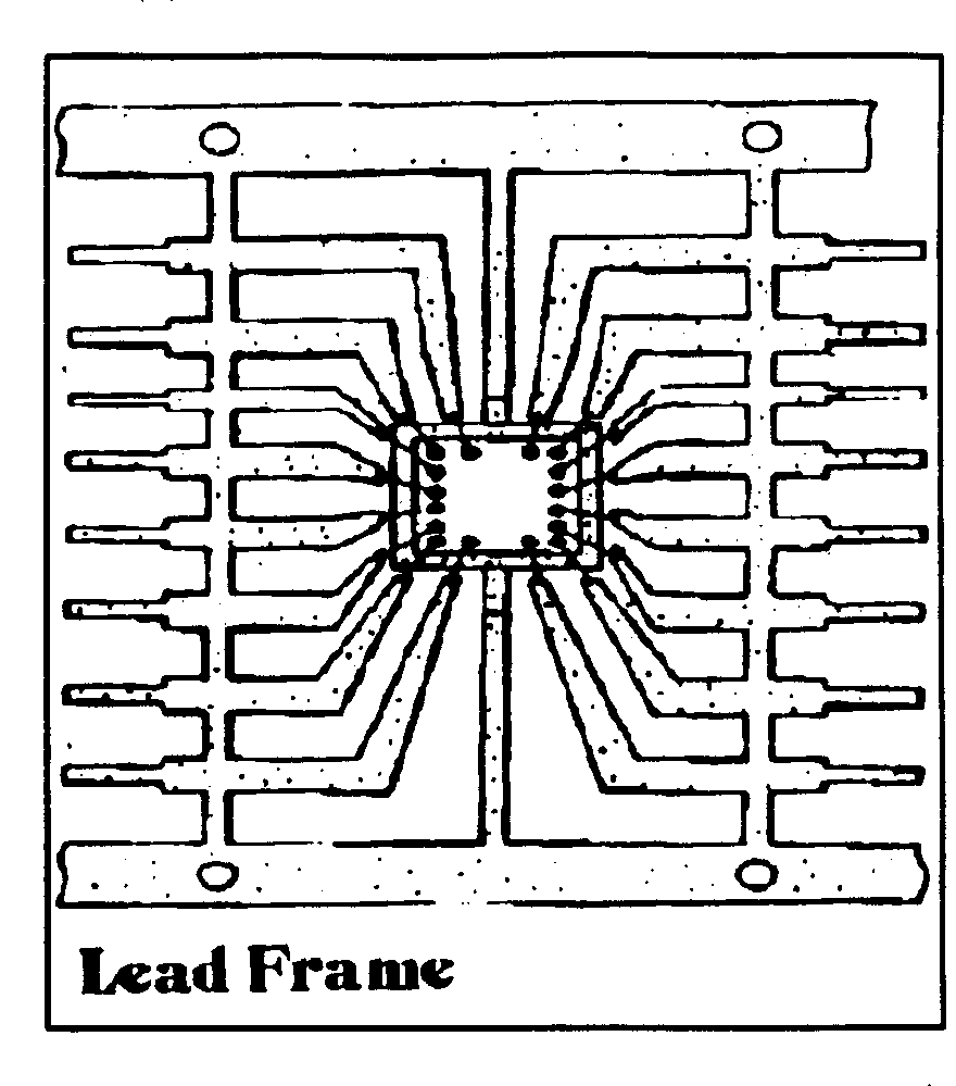
| SEE OR SEARCH CLASS:
| 29, | Metal Working,
subclasses 739+ , especially subclass 741, for means to fasten electrical
component to wiring means, base, or substrate, including a multi-lead
component; and subclass 834 for beam lead frames or beam lead devices. |
| 174, | Electricity: Conductors and Insulators,
subclass 529 for flat pack electronic device mounting means. |
| 361, | Electricity: Electrical Systems and Devices,
subclass 813 for lead frames, per se, not associated with a
solid-state active electronic device of the type classified in Class
257. |
| 428, | Stock Material or Miscellaneous Articles,
subclasses 571+ for stock materials of metal which have marginal indexing
features or weakened portion for severing. Lead frames are commonly
made in long strips of repeating patterns with such indexing and/or severing
features. |
| 438, | Semiconductor Device Manufacturing: Process, particularly
subclasses 111+ and 123+ for methods of packaging utilizing
a lead frame; see the search notes therein. |
|
| | |
| 667 | With dam or vent for encapsulant: |
| | This subclass is indented under subclass 666. Subject matter with a portion or portions to block encapsulant
flow, typically from flowing out of a mold during an encapsulation
process, or vent means (e.g., grooves in lead frame leads) to permit
egress to the atmosphere for air or other gases which are inside
a mold during encapsulation. |
| | |
| 668 | On insulating carrier other than a printed circuit board: |
| | This subclass is indented under subclass 666. Subject matter wherein the lead frame is mounted on an insulating
carrier other than a printed circuit board.
| | (1)
Note. Printed circuit boards alone, or with one or more solid-state
electronic devices mounted thereon are not classified herein, but
are found in Class 174, Electricity: Conductors and Insulators, or
Class 361, Electricity: Electrical Systems and Devices. See the
class definitions for Classes 174 and 361 for the line of demarkation
between these two classes. |
SEE OR SEARCH CLASS:
| 174, | Electricity: Conductors and Insulators,
subclasses 260 and 520 for printed circuit boards in combination with
one or more electronic solid-state devices. |
|
| | |
| 669 | With stress relief: |
| | This subclass is indented under subclass 666. Subject matter wherein means are provided to alleviate stresses
and strains (e.g., mechanical or thermal stresses) to which a lead
frame is subjected. |
| | |
| 670 | With separate tie bar element or plural tie bars: |
| | This subclass is indented under subclass 666. Subject matter in which a frame element used to tie or connect
a semiconductor chip pad/flag and/or lead fingers
frame members is a separate element and not part of the lead frame itself
or wherein plural tie bar elements are provided as part of a lead
frame. |
| | |
| 671 | Of insulating material: |
| | This subclass is indented under subclass 670. Subject matter wherein the separate tie bar element or
the plural tie bars are made of electrically insulating material. |
| | |
| 674 | With means for controlling lead tension: |
| | This subclass is indented under subclass 666. Subject matter wherein means are provided for controlling
the tension under which an electrical lead is placed including,
for example, a bend in the lead, an area of reduced lead thickness,
etc. |
| | |
| 675 | With heat sink means: |
| | This subclass is indented under subclass 666. Subject matter wherein a heat sink means is provided, either
as part of the lead frame or in addition to the lead frame for cooling
the active solid-state device. |
| | |
| 678 | HOUSING OR PACKAGE: |
| | This subclass is indented under the class definition. Subject matter wherein preformed physical means to cover
or protect a solid-state electronic device is provided therefor.
SEE OR SEARCH THIS CLASS, SUBCLASS:
| 81, | and 82, for a light emitting device in combination
with or also constituting a light responsive device and with specific
housing structure. |
| 99, | for light emitting device with specific housing
structure. |
| 177, | through 182, for a regenerative type switching device
with housing or external electrode. |
| 433, | and 434, for light responsive device with housing
or encapsulation means. |
| 573, | for Darlington configuration bipolar transistor
structure with housing or contact structure. |
| 584, | for enlarged emitter device bipolar transistor means
having housing or contact. |
| 602, | for a voltage variable capacitance device with specified
housing or contact. |
| 660, | for means to shield a device contained in a housing. |
SEE OR SEARCH CLASS:
| 361, | Electricity: Electrical Systems and Devices,
subclass 679.01 for housings and mounting assemblies for electronic
devices and components. |
| 438, | Semiconductor Device Manufacturing: Process, particularly
subclasses 106+ for methods of packaging; see the search notes
therein. |
|
| | |
| 679 | Smart (e.g., credit) card package: |
| | Subject matter under 678 wherein the housing or package
is in a form which permits it to be used as a credit card.
| | (1)
Note. A smart card is one which contains a microprocessor
chip. |
SEE OR SEARCH CLASS:
| 235, | Registers,
subclass 487 and indented subclasses for coded records including
electronic credit cards, per se. |
| 361, | Electricity: Electrical Systems and Devices,
subclasses 736+ and 752+ for modules for printed circuits
or housing or chassis for printed circuit boards. |
|
| | |
| 680 | With window means: |
| | Subject matter under 678 wherein the housing or package
has a physical opening or area otherwise transparent to ultraviolet,
visible, or infrared light. |
| | |
| 681 | For erasing EPROM: |
| | This subclass is indented under subclass 680. Subject matter wherein the window means is provided for
transmitting light to erase an electrically programmable read-only
memory (EPROM). |
| | |
| 682 | With desiccant, getter, or gas filling: |
| | This subclass is indented under subclass 678. Subject matter including a desiccant (i.e., a material for
absorbing moisture); a getter (i.e., a material which absorbs undesirable
semiconductor, housing or package contaminants); or wherein a gaseous
material fills the housing or package. |
| | |
| 684 | With semiconductor element forming part (e.g., base, of
housing): |
| | This subclass is indented under subclass 678. Subject matter wherein part of the housing is formed by
a semiconductor element.
| | (1)
Note. The semiconductor element may have an inactive portion
connected to the rest of the housing, and another portion forming
an active device, for example. Frequently the semiconductor element forms
the base of the housing, through which leads are inserted. | |
| | |
| 685 | Multiple housings: |
| | This subclass is indented under subclass 678. Subject matter wherein more than one housing is provided
for a solid-state active electronic device, or wherein plural housings,
each containing one or more solid-state active devices, are constructed
as a unitary structure.
| | (1)
Note. One housing may be located within another housing. | |
| | |
| 687 | Housing or package filled with solid or liquid electrically
insulating material: |
| | This subclass is indented under subclass 678. Subject matter wherein the housing or package is filled
with a solid or liquid electrically insulating material.
| | (1)
Note. Encapsulated devices are excluded from this subclass
and are not considered to be housings or packages as defined in
subclass 678 which requires them to be preformed. |
SEE OR SEARCH CLASS:
| 361, | Electricity: Electrical Systems and Devices,
subclasses 729 , 730+, and 744+ for various modules
for printed circuit boards. |
|
| | |
| 689 | Rigid electrode portion: |
| | This subclass is indented under subclass 688. Subject matter wherein the large area electrodes are rigid
in whole or in part.
| | (1)
Note. These type devices typically employ relatively massive
electrodes to operate at large current densities. | |
| | |
| 690 | With contact or lead: |
| | This subclass is indented under subclass 678. Subject matter wherein the device is provided with a contact
or lead, in addition to or as part of the package or housing. |
| | |
| 692 | With particular lead geometry: |
| | This subclass is indented under subclass 690. Subject matter wherein the contact or lead provided as part
of or in addition to the package or housing has a specified geometrical
configuration. |
| | |
| 693 | External connection to housing: |
| | This subclass is indented under subclass 692. Subject matter wherein the contact or lead having a specified
geometry comprises an electrical connection for connecting the package
or housing and its contained active solid-state device to other
electrical devices or circuits. |
| | |
| 694 | Axial leads: |
| | This subclass is indented under subclass 693. Subject matter wherein the leads or contacts which form
an external connection to the housing or package extend out opposite
ends along an axis of symmetry of a housing or package. |
| | |
| 695 | Fanned/radial leads: |
| | This subclass is indented under subclass 693. Subject matter wherein the leads or contacts which form
an external connection to the housing or package extend radially
outward from the package.
| | (1)
Note. See illustration, below.
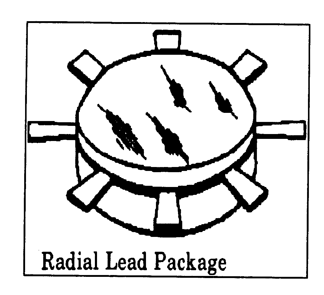
| |
| | |
| 696 | Bent (e.g., J-shaped) lead: |
| | This subclass is indented under subclass 693. Subject matter wherein the leads or contacts which form
an external connection to the housing or package include one or
more leads which have a curved end portion (e.g., for mounting on
the top surface of a printed circuit board).
| | (1)
Note. See illustration, below.
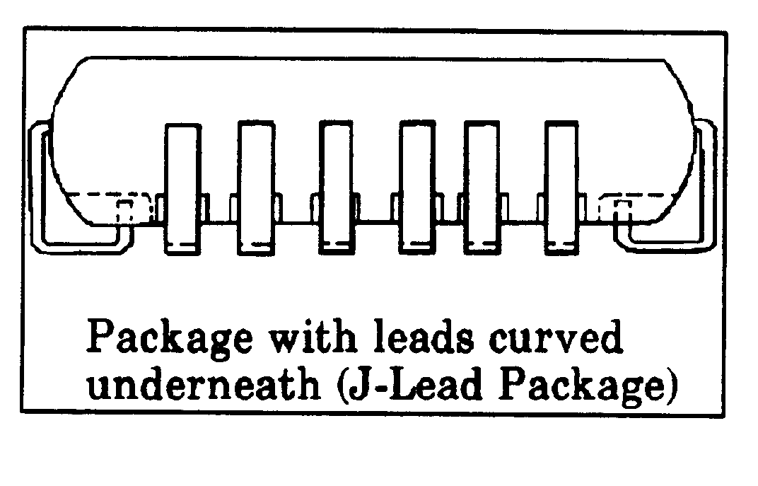
| |
| | |
| 697 | Pin grid type: |
| | This subclass is indented under subclass 693. Subject matter wherein the leads or contacts which form
an external connection to the housing or package are in the form
of a grid or matrix of elongated pins.
| | (1)
Note. See illustration, below.
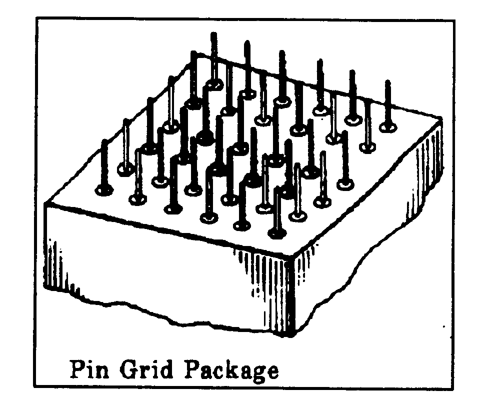
| |
| | |
| 699 | Housing entirely of metal except for feedthrough structure: |
| | Subject matter under 698 wherein the housing or package
is made entirely of metal except for the portion wherein the electrical
contacts or leads are fed through.
| | (1)
Note. Typically, an insulator is placed in the feedthrough
portion of a metal housing to prevent electrical short circuiting of
the leads to the housing. | |
| | |
| 702 | Of insulating material other than ceramic: |
| | Subject matter under 701 wherein the housing is made of
electrically insulating material other than ceramic (e.g., the housing
is made of glass or of a single crystal insulator material).
| | (1)
Note. A ceramic is a polycrystalline, non-metallic, non-organic
material, such as fired polycrystalline aluminum oxide, typically
made by firing a compressed and shaped powder at high temperatures to
fuse the powder together. | |
| | |
| 704 | Cap or lid: |
| | This subclass is indented under subclass 701. Subject matter wherein the housing or package is provided
with a cap or lid. |
| | |
| 706 | With heat sink: |
| | This subclass is indented under subclass 701. Subject matter wherein the insulating housing has a heat
sink to dissipate heat.
| | (1)
Note. The heat sink may be located in a cavity in a base
member made of ceramic material. |
SEE OR SEARCH CLASS:
| 174, | Electricity: Conductors and Insulators, appropriate subclasses directed to cooling means. |
| 361, | Electricity: Electrical Systems and Devices,
subclasses 688 through 723for cooling means for electronic devices or components
with housings or mounting assemblies. |
|
| | |
| 708 | Entirely of metal except for feedthrough: |
| | This subclass is indented under subclass 678. Subject matter wherein the housing or package is made entirely
of metal except for the portion wherein the electrical contacts
or leads are fed through.
| | (1)
Note. Typically, an insulator is placed in the feedthrough
portion of a metal housing to prevent electrical short circuiting of
the leads to the housing. | |
| | |
| 709 | With specified insulator to isolate device from housing: |
| | This subclass is indented under subclass 708. Subject matter wherein a specific insulator means is provided
to electrically isolate the active solid-state device contained
in the metal package or housing from the metal package or housing
to prevent electrical short circuits due to the housing or package. |
| | |
| 712 | With provision for cooling the housing or its contents: |
| | This subclass is indented under subclass 678. Subject matter wherein means for cooling the housing or
its contents are provided in addition to natural cooling processes.
SEE OR SEARCH CLASS:
| 174, | Electricity: Conductors and Insulators, appropriate subclasses directed to cooling means. |
| 361, | Electricity: Electrical Systems and Devices,
subclasses 688 through 723,for cooling means for electronic devices or components
with housings or mounting assemblies. |
|
| | |
| 713 | For integrated circuit: |
| | This subclass is indented under subclass 712. Subject matter wherein the solid-state electronic device
for which cooling means is provided is an integrated circuit, which
is a semiconductor substrate which contains a plurality of active
solid-state electronic devices. |
| | |
| 714 | Liquid coolant: |
| | This subclass is indented under subclass 712. Subject matter wherein the means provided for cooling the
housing or its contents is a liquid. |
| | |
| 715 | Boiling (evaporative) liquid: |
| | This subclass is indented under subclass 714. Subject matter wherein the cooling means involves boiling
a liquid to provide evaporative cooling.
SEE OR SEARCH CLASS:
| 174, | Electricity: Conductors and Insulators, appropriate subclasses directed to liquid cooling
means. |
| 361, | Electricity: Electrical Systems and Devices,
subclasses 699+ for liquid cooling means for electronic devices or
components with housings or mounting assemblies. |
|
| | |
| 716 | Cryogenic liquid coolant: |
| | This subclass is indented under subclass 714. Subject matter wherein the cooling means uses a liquid to
maintain device temperatures at or below 100 degrees Kelvin.
SEE OR SEARCH CLASS:
| 174, | Electricity: Conductors and Insulators, appropriate subclasses directed to liquid cooling
means. |
| 361, | Electricity: Electrical Systems and Devices,
subclasses 699+ for liquid cooling means for electronic devices or
components with housings or mounting assemblies. |
|
| | |
| 721 | With gas coolant: |
| | This subclass is indented under subclass 712. Subject matter wherein the cooling means uses a gas to provide
the cooling (e.g., by convection). |
| | |
| 722 | With fins: |
| | This subclass is indented under subclass 721. Subject matter wherein the cooling means has fins, i.e.,
long, thin, blade like structures used to dissipate heat to the
gas coolant. |
| | |
| 723 | For plural devices: |
| | This subclass is indented under subclass 678. Subject matter wherein a package or housing is provided
for more than one electronic device, at least one of the electronic
devices being an active solid-state device.
SEE OR SEARCH CLASS:
| 174, | Electricity: Conductors and Insulators,
subclasses 50+ for housings and printed circuits. |
| 361, | Electricity: Electrical Systems and Devices,
subclasses 729 and 730+ for plural housing modules. |
|
| | |
| 724 | With discrete components: |
| | This subclass is indented under subclass 723. Subject matter wherein at least some of the electronic components
are in the form of an individual device per semiconductor chip,
as contrasted to a single integrated circuit containing plural semiconductor
devices. The discrete components may be active solid-state devices or
passive components such as resistors, capacitors, or inductors. |
| | |
| 728 | For high frequency (e.g., microwave) device: |
| | This subclass is indented under subclass 678. Subject matter wherein the active solid-state device provided
with a housing or package is a high frequency solid-state electronic
device operating at high frequencies, such as microwave frequencies
or above. |
| | |
| 731 | With housing mount: |
| | This subclass is indented under subclass 678. Subject matter wherein the housing or package has means
(e.g., a flange or threaded stud) for attaching the housing to a
support.
| | (1)
Note. Search this class, subclass 180 for housings or packages
of this type which specifically contain a regenerative type switching
device such as an SCR or thyristor. | |
| | |
| 732 | Flanged mount: |
| | This subclass is indented under subclass 731. Subject matter wherein the housing mount is a flange with
openings therein (e.g., threaded holes) to permit the housing to
be attached (e.g., by fasteners) to a support. |
| | |
| 733 | Stud mount: |
| | This subclass is indented under subclass 731. Subject matter wherein the housing mount is a threaded element
shaped like a bolt extending from the housing for fastening into
a threaded hole in a support. |
| | |
| 734 | COMBINED WITH ELECTRICAL CONTACT OR LEAD: |
| | This subclass is indented under the class definition. Subject matter wherein the active solid-state device is
provided with one or more electrical contacts or leads.
SEE OR SEARCH THIS CLASS, SUBCLASS:
| 41, | for point contact rectifiers. |
| 44, | through 47, for devices with a metal contact alloyed
to elemental semiconductor type PN junction in a non-regenerative
structure. |
| 54, | for Schottky barrier to amorphous semiconductor
material device. |
| 73, | for Schottky barrier to polycrystalline semiconductor
material device. |
| 81, | and 82, for light emitter combined with or also
constituting a light responsive device and having a specific housing
or contact structure. |
| 91, | for plural light emitting devices with shaped contacts
or opaque masking. |
| 99, | for light emitting devices with specified housing
or contact structure. |
| 145, | for a regenerative type device combined with a FET
with extended latching current level and a low impedance channel
contact extending below the device surface. |
| 155, | and 156, for a regenerative type device with switching
speed enhancing means (e.g., a Schottky contact). |
| 177, | through 182, for a regenerative type device with
housing or external electrode. |
| 217, | for a majority signal carrier charge transfer device
with a conductive means in direct contact with channel (e.g., a
non-insulated gate). |
| 260, | for JFET having the same channel controlled by,
for example, Schottky barrier and pn junction gates. |
| 276, | for a JFET in a microwave integrated circuit with
a contact or heat sink extending through a hole in the semiconductor. |
| 280, | through 284, for JFETs with a Schottky gate electrode. |
| 316, | through 322, for a variable threshold insulated
electrical field effect device with additional contacted control
electrode. |
| 343, | for graded channel dopant IGFET device with plural
sections connected in parallel and having all contacts on the same
surface. |
| 382, | through 385, for an IGFET in an integrated circuit
with a refractory material contact to source or drain region. |
| 449, | through 457, for Schottky contacts in light responsive
devices. |
| 471, | through 486, for Schottky contact devices. |
| 502, | for high power integrated circuit devices with electrical
isolation and a backside collector contact. |
| 503, | for an integrated circuit device with electrically
isolated components having a contact or metallization configuration
to reduce parasitic coupling. |
| 522, | for beam-lead supported semiconductor islands in
integrated circuits. |
| 573, | for Darlington configuration non-isolated bipolar
transistors with resistance means connected between transistor base
regions and with housing or contact structure or configuration. |
| 576, | for complementary bipolar transistors sharing a
common active region (e.g., IIL, I2L) including
lateral bipolar transistor structure and having contacts of a refractory
material. |
| 584, | for bipolar transistor device with enlarged emitter
area and with housing or contact means. |
| 602, | for a voltage variable capacitance device with specified
housing or contact. |
| 621, | for a semiconductor device with electrical contact
in a hole in the semiconductor (e.g., lead extends through semiconductor
body). |
| 624, | for mesa structure device having a low resistance
ohmic connection along a mesa edge. |
| 661, | through 663, for superconductive contacts or leads. |
| 664, | for transmission line leads. |
| 665, | for contacts or leads including fusible link or
noise suppression means. |
| 666, | through 677, for lead frames. |
| 688, | and 689, for housings with large area flexible electrodes
in press contact with opposite sides of active semiconductor chip
and surrounded by an insulating element. |
| 690, | through 700, for housings with specified contact
or lead. |
| 905, | for plural DRAM cells sharing a common contact or
common trench. |
| 926, | for a device with an elongated lead extending axially
through another elongated lead. |
| 928, | for shorted pn or Schottky junction other than an
emitter junction. |
SEE OR SEARCH CLASS:
| 174, | Electricity: Conductors and Insulators,
subclasses 99+ for bus bar structure, per se. |
| 361, | Electricity: Electrical Systems and Devices,
subclasses 772 through 776for specific lead configurations connecting electronic
systems and devices to printed circuit boards. |
|
| | |
| 735 | Beam leads (i.e., leads that extend beyond the ends or
sides of a chip component): |
| | This subclass is indented under subclass 734. Subject matter wherein electrical contact leads extend like
beams beyond the ends of a chip component.
SEE OR SEARCH CLASS:
| 438, | Semiconductor Device Manufacturing: Process, particularly
subclass 411 for methods of forming electrically isolated semiconductor
islands held in place by beam lead metallization; subclass 461 for
methods of forming beam leads on a semiconductor substrate combined
with dicing of the substrate into plural separate bodies; and subclass
611 for methods of forming beam lead metallization on a semiconductor
substrate. |
|
| | |
| 736 | Layered: |
| | This subclass is indented under subclass 735. Subject matter wherein the leads are made of at least two
separate layers of the same or different material. |
| | |
| 737 | Bump leads: |
| | This subclass is indented under subclass 734. Subject matter wherein an electrical contact is in the form
of a relatively abrupt protuberance on the surface of a solid-state
electronic device or chip/die containing such a device. |
| | |
| 738 | Ball shaped: |
| | This subclass is indented under subclass 737. Subject matter wherein the bump contacts have the spherical
shape of a ball.
SEE OR SEARCH THIS CLASS, SUBCLASS:
| 780, | for ball shaped bonds, generally. |
|
| | |
| 739 | With textured surface: |
| | This subclass is indented under subclass 734. Subject matter wherein the surface of the contact or lead
is rough or has a characteristic of a closely interwoven fabric,
rather than being smooth. |
| | |
| 743 | For compound semiconductor material: |
| | This subclass is indented under subclass 742. Subject matter in which the electrical contact material
contacts and contains a dopant for a semiconductor material which
is a chemical compound, as contrasted to an elemental semiconductor. |
| | |
| 745 | Contact for III-V material: |
| | This subclass is indented under subclass 744. Subject matter in which the compound semiconductor material
is a group III-V compound, i.e., one component is from periodic
table group III and the other is from periodic table group V. |
| | |
| 747 | With thermal expansion matching of contact or lead material
to semiconductor active device: |
| | This subclass is indented under subclass 741. Subject matter in which the electrical contact or lead material
is chosen to have a coefficient of thermal expansion which closely
matches that of the semiconductor active device material.
SEE OR SEARCH THIS CLASS, SUBCLASS:
| 178, | for regenerative device with housing and means to
avoid stress (e.g., thermal matching of electrode to semiconductor). |
| 633, | for thermal expansion compensation between semiconductor
and insulating coating. |
|
| | |
| 750 | Layered: |
| | This subclass is indented under subclass 741. Subject matter wherein the specified contact material is
layered. |
| | |
| 751 | At least one layer forms a diffusion barrier: |
| | This subclass is indented under subclass 750. Subject matter wherein at least one layer forms a barrier
to the diffusion of the contact material into the semiconductor
or into another contact layer.
SEE OR SEARCH THIS CLASS, SUBCLASS:
| 486, | for Schottky barrier layers including a diffusion
barrier material. |
|
| | |
| 754 | At least one layer of silicide or polycrystalline silicon: |
| | This subclass is indented under subclass 750. Subject matter wherein at least one layer of material is
made up of a silicide or polycrystalline silicon.
SEE OR SEARCH THIS CLASS, SUBCLASS:
| 381, | and 538, for polycrystalline silicon resistive elements
connected to active semiconductor electronic devices. |
| 554, | and 588, for bipolar transistor devices with a polycrystalline
semiconductor connection electrode. |
|
| | |
| 755 | Polysilicon laminated with silicide: |
| | This subclass is indented under subclass 754. Subject matter wherein the layers include a polysilicon
laminated with a silicide.
| | (1)
Note. Such laminated contacts of polysilicon and silicide
are sometimes called "polycide" contacts. | |
| | |
| 757 | Silicide of refractory or platinum group metal: |
| | This subclass is indented under subclass 754. Subject matter wherein a layered electrical contact or lead
includes a silicide of a metal found in groups IVA, VA, VIA or VIIIA
(other than iron (Fe), nickel (Ni) or cobalt (Co)) of the periodic
table of the elements. |
| | |
| 758 | Multiple metal levels on semiconductor, separated by insulating
layer (e.g., multiple level metallization for integrated circuit): |
| | This subclass is indented under subclass 750. Subject matter wherein there are plural layers of metal
forming electrical contact material, the layers being separated
by intervening layers of insulator material.
SEE OR SEARCH THIS CLASS, SUBCLASS:
| 211, | for gate arrays with multi-level metallization. |
SEE OR SEARCH CLASS:
| 156, | Adhesive Bonding and Miscellaneous Chemical Manufacture,
subclasses 60+ , for processes of uniting plural bodies via an
adhesive material. |
| 438, | Semiconductor Device Manufacturing: Process, particularly
subclasses 118+ for methods of packaging a semiconductor device
including a step of bonding utilizing an adhesive material; see
the search notes therein. |
|
| | |
| 759 | Including organic insulating material between metal levels: |
| | This subclass is indented under subclass 758. Subject matter wherein there is at least one layer of organic
insulating material between different layers of metal. An organic
compound is one which fulfills the requirements of the Class 260
definition, i.e., has a molecule characterized by two carbon atoms
bonded together, one atom of carbon being bonded to at least one
atom of hydrogen or a halogen, or one atom or carbon bonded to at
least one atom of nitrogen by a single or double bond, certain compounds
such as HCN, CN-CN, HNCO, HNCS, cyanogen halides, cyanamide, fulminic
acid and metal carbides, being exceptions to this rule. |
| | |
| 768 | Refractory or platinum group metal or alloy or silicide
thereof: |
| | This subclass is indented under subclass 741. Subject matter wherein the specified contact or lead material
is a refractory metal or a platinum group metal, i.e., a metal found
in groups IVA, VA, VIA or VIIIA (other than iron (Fe), nickel (Ni)
or cobalt (Co)) of the periodic table of the elements or a silicide
(i.e., a binary compound of silicon), usually with a more electropositive element
or radical, thereof. |
| | |
| 769 | Platinum group metal or silicide thereof: |
| | This subclass is indented under subclass 768. Subject matter wherein the specified contact or lead material
is a platinum group metal (i.e., platinum (Pt), palladium (Pd),
rhodium (Rh), ruthenium (Ru), osmium (Os) or iridium (Ir)) or a
silicide i.e., a binary compound of silicon, usually with a more
electropositive element or radical, thereof. |
| | |
| 772 | Solder composition: |
| | This subclass is indented under subclass 741. Subject matter wherein the specific contact or lead material
is a solder composition (i.e., a metal or metallic alloy that melts
at relatively low temperatures).
| | (1)
Note. Solder is normally used to join metals with higher
melting points than the solder composition. | |
| | |
| 774 | Via (interconnection hole) shape: |
| | This subclass is indented under subclass 773. Subject matter wherein the shape or configuration of an
electrical contact or lead is determined by the shape of a hole
through an insulating layer through which the contact extends. |
| | |
| 776 | Cross-over arrangement, component or structure: |
| | This subclass is indented under subclass 773. Subject matter wherein means are provided for electrically
insulating electrical contact elements or leads which cross each
other to do so without a short circuit therebetween.
| | (1)
Note. Electrically insulating components or structures associated
with electrical contact crossovers may be referred to as bridges,
tunnels, overpasses, underpasses, etc. | |
| | |
| 777 | Chip mounted on chip: |
| | This subclass is indented under subclass 734. Subject matter wherein a semiconductor substrate of an active
solid-state device is electrically connected to, and positioned
on, another semiconductor substrate.
SEE OR SEARCH CLASS:
| 361, | Electricity: Electrical Systems and Devices,
subclasses 760+ for plural modules or means of connection of components
to a printed circuit board. |
|
| | |
| 778 | Flip chip: |
| | This subclass is indented under subclass 734. Subject matter wherein a semiconductor substrate which contains
an active solid-state electronic device has electric contacts on
the top side thereof, the top side being that which contains an
active solid-state electronic device, and which is flipped so that
the contact side becomes the bottom side for connection with a substrate
which has matching electrical contacts. |
| | |
| 780 | Ball or nail head type contact, lead, or bond: |
| | This subclass is indented under subclass 734. Subject matter wherein a contact, lead, or bond is in the
form of a wire having an end for connection to the semiconductor
which is in the shape of a ball or nail head.
SEE OR SEARCH THIS CLASS, SUBCLASS:
| 738, | for ball shaped bump contacts. |
|
| | |
| 782 | Die bond: |
| | This subclass is indented under subclass 734. Subject matter wherein a semiconductor chip containing at
least one active solid-state device and provided with a contact
or lead is provided with a means for attaching the chip to a supporting
member.
| | (1)
Note. The supporting member or attachment may form part of
the contacts or leads for the chip, or be separate therefrom. | |
| | |
| 783 | With adhesive means: |
| | This subclass is indented under subclass 782. Subject matter wherein adhesive means (e.g., a layer) is
provided to secure a die (chip) which contains an active solid-state
electronic device to a supporting member.
SEE OR SEARCH CLASS:
| 156, | Adhesive Bonding and Miscellaneous Chemical Manufacture,
subclasses 60+ for processes of uniting plural bodies via an adhesive
material. |
| 438, | Semiconductor Device Manufacturing: Process, particularly
subclasses 118+ for methods of packaging a semiconductor device
including a step of bonding utilizing an adhesive material; see
the search notes therein. |
|
| | |
| 784 | Wire contact, lead, or bond: |
| | This subclass is indented under subclass 734. Subject matter wherein the contact, lead or bond is a very
flexible, elongated, small diameter filament made of electrically
conductive material. |
| | |
| 785 | By pressure alone: |
| | This subclass is indented under subclass 734. Subject matter wherein the electrical contact, lead or bond
is held in place by pressure alone (e.g., by a spring clip).
SEE OR SEARCH THIS CLASS, SUBCLASS:
| 181+, | and 688+, for other electrodes in press contact
with an active semiconductor device. |
|
| | |
| 786 | Configuration or pattern of bonds: |
| | This subclass is indented under subclass 734. Subject matter wherein the electrical contact, lead or bond,
has a specific configuration or pattern.
SEE OR SEARCH THIS CLASS, SUBCLASS:
| 459, | for light activated devices with particular bonding
pad arrangement. |
| 625, | for mesa structure semiconductor device bonded to
heat sink or thick electrical conductor. |
|
| | |
| 787 | ENCAPSULATED: |
| | This subclass is indented under the class definition. Subject matter wherein an active solid-state electronic
device, often part of a semiconductor chip, is surrounded by an
electrically insulating material which forms a sealed encasement
therefor.
SEE OR SEARCH THIS CLASS, SUBCLASS:
| 100, | for encapsulated light emitter device. |
| 433+, | for light responsive devices with housing or encapsulation. |
| 687, | for a housing containing an encapsulant material. |
SEE OR SEARCH CLASS:
| 29, | Metal Working, particularly
subclasses 841 and 855 for methods of assembling an electrical
component to a base or lead and encapsulating the same. |
| 65, | Glass Manufacturing, appropriate subclasses for the manufacturing of glass
encapsulated electronic devices or components thereof. |
| 174, | Electricity: Conductors and Insulators,
subclass 251 for a printed circuit with an encapsulated wire. |
| 264, | Plastic and Nonmetallic Article Shaping or Treating:
Processes,
subclass 272.11 for encapsulation of electrical components. |
| 343, | Communications: Radio Wave Antennas,
subclass 873 for embedded, potted, or coated radio wave antennas. |
| 361, | Electricity: Electrical Systems and Devices,
subclasses 600 and 679.01 for enclosures, including encapsulated types,
for electrical and electronic devices. |
| 438, | Semiconductor Device Manufacturing: Process, particularly
subclasses 112 and 127 for methods of encapsulating; see the search
notes therein. |
|
| | |
| 788 | With specified encapsulant: |
| | This subclass is indented under subclass 787. Subject matter wherein the chemical composition of the material
that encapsulates the active solid-state electronic device is specified. |
| | |
| 789 | With specified filler material: |
| | This subclass is indented under subclass 788. Subject matter wherein a particular material has been added
to an encapsulant material to give it desirable mechanical, thermal,
electrical, or other desirable characteristics, and the material
is specified. |
| | |
| 791 | Including polysiloxane (e.g., silicone resin): |
| | This subclass is indented under subclass 788. Subject matter wherein the encapsulant includes polysiloxane
(i.e., any of various polymeric compounds which contain alternate silicon
and oxygen atoms in either a linear or cyclic arrangement), often
with one or two organic groups attached to each silicon atom. |
| | |
| 792 | Including polyimide: |
| | This subclass is indented under subclass 788. Subject matter wherein the encapsulant includes polyimide
i.e., a polymeric compound resulting from replacement of both atoms
of hydrogen in an organic amine by organic univalent acid radicals
or by an organic divalent acid radical.
| | (1)
Note. Polyimides are copolymers (polymers formed from at
least two different starting organic materials) which have a linkage,
as illustrated below, between the starting materials, wherein R
is typically hydrogen and Q1 and Q2 are
the organic residues of the starting monomers. | |
| | |
| 793 | Including epoxide: |
| | This subclass is indented under subclass 788. Subject matter wherein the encapsulant includes an epoxy
compound (i.e., a compound containing three membered ring consisting
or one oxygen and two carbon atoms). |
| | |
| 794 | Including glass: |
| | This subclass is indented under subclass 788. Subject matter wherein the encapsulant contains glass (i.e.,
an amorphous inorganic, usually transparent or translucent substance consisting
of a mixture of silicates or borates or phosphates formed by fusion
of silica or of oxides of boron or phosphorous with a flux and stabilizer
that cools to a rigid condition without crystallization). |
| | |
| 795 | With specified filler material: |
| | This subclass is indented under subclass 787. Subject matter wherein a particular material has been added
to an encapsulant material to give it desirable mechanical, thermal,
electrical, or other desirable characteristics, and the material
is specified. |
| | |
| 796 | With heat sink embedded in encapsulant: |
| | This subclass is indented under subclass 787. Subject matter wherein a heat sink is embedded in the encapsulant.
SEE OR SEARCH CLASS:
| 174, | Electricity: Conductors and Insulators, appropriate subclasses. |
| 361, | Electricity: Electrical Systems and Devices,
subclasses 704 through 723 for thermal conduction means. |
|
| | |
| 797 | ALIGNMENT MARKS: |
| | This subclass is indented under the class definition. Subject matter wherein the active solid-state device is
provided with one or more indicia or marks used during fabrication
of the device to facilitate accurate alignment of regions in the
device. |
| | |
| 798 | MISCELLANEOUS: |
| | This subclass is indented under the class definition. Subject matter wherein the subject matter is not otherwise
provided for. |
| | |
E-SUBCLASSES
The E-subclasses in U.S. Class 257 provide for active solid-state
electronic devices, that is, electronic devices or components that
are made primarily of solid materials, usually semiconductors, which
operate by the movement of charge carriers - electrons or holes
- which undergo energy level changes within the material and can
modify an input voltage or electro-magnetic signal to achieve rectification,
amplification, oscillating, radiation emission, or switching action,
or capacitors or resistors with potential-jump or surface barrier;
the E-subclasses include processes or apparatus peculiar to the manufacture
or treatment of such active solid-state devices or of parts of such
devices.
| E21.001 | PROCESSES OR APPARATUS ADAPTED FOR MANUFACTURE OR TREATMENT OF
SEMICONDUCTOR OR SOLID-STATE DEVICES OR OF PARTS THEREOF (EPO): |
| | This main group provides for processes or apparatus that
are employed in the manufacture or treatment of semiconductor or
solid-state devices or of parts thereof. This subclass is substantially
the same in scope as ECLA classification H01L21/00.
| | (1)
Note. This subclass will take subject matter where the manufactured
or treated device/component (or part thereof) will have
at least one of the following capabilities:
| | (a)
The conduction or modification of an electrical current, |
| | (b)
The storage of electrical energy for subsequent discharge
within a microelectronic integrated circuit, or |
| | (c)
The conversion of electromagnetic wave energy to electrical
energy or electrical energy to electromagnetic energy. | |
SEE OR SEARCH THIS CLASS, SUBCLASS:
| E31.001, | E33.001, E39.001, E45.001, E47.001, E49.001, and
E51.001, for processes or apparatus adapted for manufacture or treatment
of semiconductor or solid state devices or of parts thereof. |
|
| | |
| E21.004 | Of resistor (EPO): |
| | This subclass is indented under subclass E21.003. This subclass
is substantially the same in scope as ECLA classification H01L21/02B2. |
| | |
| E21.008 | Of capacitor (EPO): |
| | This subclass is indented under subclass E21.003. This subclass
is substantially the same in scope as ECLA classification H01L21/02B3. |
| | |
| E21.022 | Of inductor (EPO): |
| | This subclass is indented under subclass E21.003. This subclass
is substantially the same in scope as ECLA classification H01L21/02B4. |
| | |
| E21.025 | For lift-off process (EPO): |
| | This subclass is indented under subclass E21.024. This subclass
is substantially the same in scope as ECLA classification H01L21/027B2. |
| | |
| E21.028 | Using laser (EPO): |
| | This subclass is indented under subclass E21.027. This subclass
is substantially the same in scope as ECLA classification H01L21/027B6B2. |
| | |
| E21.045 | Making electrode (EPO): |
| | This subclass is indented under subclass E21.041. This subclass
is substantially the same in scope as ECLA classification H01L21/04D20. |
| | |
| E21.046 | Ohmic electrode (EPO): |
| | This subclass is indented under subclass E21.045. This subclass
is substantially the same in scope as ECLA classification H01L21/04D20A. |
| | |
| E21.047 | Schottky electrode (EPO): |
| | This subclass is indented under subclass E21.045. This subclass
is substantially the same in scope as ECLA classification H01L21/04D20C. |
| | |
| E21.053 | Diode (EPO): |
| | This subclass is indented under subclass E21.052. This subclass
is substantially the same in scope as ECLA classification H01L21/04D40C2. |
| | |
| E21.057 | Using ion implantation (EPO): |
| | This subclass is indented under subclass E21.056. This subclass
is substantially the same in scope as ECLA classification H01L21/04H4A.
SEE OR SEARCH THIS CLASS, SUBCLASS:
| E21.054, | for processes where ion implantation of boron and
subsequent annealing does not produce a p-doped region. |
|
| | |
| E21.058 | Using masks (EPO): |
| | This subclass is indented under subclass E21.057. This subclass
is substantially the same in scope as ECLA classification H01L21/04H4A10. |
| | |
| E21.059 | Angled implantation (EPO): |
| | This subclass is indented under subclass E21.057. This subclass
is substantially the same in scope as ECLA classification H01L21/04H4A12. |
| | |
| E21.061 | Making electrode (EPO): |
| | This subclass is indented under subclass E21.054. This subclass
is substantially the same in scope as ECLA classification H01L21/04H10. |
| | |
| E21.062 | Ohmic electrode (EPO): |
| | This subclass is indented under subclass E21.061. This subclass
is substantially the same in scope as ECLA classification H01L21/04H10A. |
| | |
| E21.064 | Schottky electrode (EPO): |
| | This subclass is indented under subclass E21.061. This subclass
is substantially the same in scope as ECLA classification H01L21/04H10C. |
| | |
| E21.077 | Heat treating (EPO): |
| | This subclass is indented under subclass E21.076. This subclass
is substantially the same in scope as ECLA classification H01L21/145. |
| | |
| E21.088 | By direct bonding (EPO): |
| | This subclass is indented under subclass E21.087. This subclass
is substantially the same in scope as ECLA classification H01L21/18B2. |
| | |
| E21.124 | Heteroepitaxy (EPO): |
| | This subclass is indented under subclass E21.123. This subclass
is substantially the same in scope as ECLA classification H01L21/20B6B. |
| | |
| E21.139 | Lithium-drift (EPO): |
| | This subclass is indented under subclass E21.135. This subclass
is substantially the same in scope as ECLA classification H01L21/22L. |
| | |
| E21.14 | Diffusion source (EPO): |
| | This subclass is indented under subclass E21.135. This subclass
is substantially the same in scope as ECLA classification H01L21/22N. |
| | |
| E21.147 | By ion implantation (EPO): |
| | This subclass is indented under subclass E21.146. This subclass
is substantially the same in scope as ECLA classification H01L21/225A2D. |
| | |
| E21.161 | Of conductive layer (EPO): |
| | This subclass is indented under subclass E21.16. This subclass
is substantially the same in scope as ECLA classification H01L21/285B. |
| | |
| E21.171 | Selective deposition (EPO): |
| | This subclass is indented under subclass E21.17. This subclass
is substantially the same in scope as ECLA classification H01L21/285B4H2. |
| | |
| E21.177 | MOS-gate structure (EPO): |
| | This subclass is indented under subclass E21.176. This subclass
is substantially the same in scope as ECLA classification H01L21/28B2. |
| | |
| E21.178 | Joint-gate structure (EPO): |
| | This subclass is indented under subclass E21.177. This subclass
is substantially the same in scope as ECLA classification H01L21/28B2C. |
| | |
| E21.195 | Characterized by conductor (EPO): |
| | This subclass is indented under subclass E21.191. This subclass
is substantially the same in scope as ECLA classification H01L21/28E2B.
| | (1)
Note. This subclass includes the final conductor comprising
a superconductor. | |
| | |
| E21.219 | Chemical etching (EPO): |
| | This subclass is indented under subclass E21.215. This subclass
is substantially the same in scope as ECLA classification H01L21/306B. |
| | |
| E21.222 | Vapor phase etching (EPO): |
| | This subclass is indented under subclass E21.22. This subclass
is substantially the same in scope as ECLA classification H01L21/306B4C. |
| | |
| E21.224 | Chemical cleaning (EPO): |
| | This subclass is indented under subclass E21.215. This subclass
is substantially the same in scope as ECLA classification H01L21/306N. |
| | |
| E21.226 | Dry cleaning (EPO): |
| | This subclass is indented under subclass E21.224. This subclass
is substantially the same in scope as ECLA classification H01L21/306N2. |
| | |
| E21.228 | Wet cleaning only (EPO): |
| | This subclass is indented under subclass E21.224. This subclass
is substantially the same in scope as ECLA classification H01L21/306N4. |
| | |
| E21.231 | Using mask (EPO): |
| | This subclass is indented under subclass E21.215. This subclass
is substantially the same in scope as ECLA classification H01L21/308. |
| | |
| E21.241 | Post-treatment (EPO): |
| | This subclass is indented under subclass E21.24. This subclass
is substantially the same in scope as ECLA classification H01L21/3105. |
| | |
| E21.242 | Of organic layer (EPO): |
| | This subclass is indented under subclass E21.241. This subclass
is substantially the same in scope as ECLA classification H01L21/3105P. |
| | |
| E21.248 | By ion implantation (EPO): |
| | This subclass is indented under subclass E21.247. This
subclass is substantially the same in scope as ECLA classification
H01L21/3115B. |
| | |
| E21.251 | By chemical means (EPO): |
| | This subclass is indented under subclass E21.25. This subclass
is substantially the same in scope as ECLA classification H01L21/311B2. |
| | |
| E21.252 | By dry-etching (EPO): |
| | This subclass is indented under subclass E21.251. This
subclass is substantially the same in scope as ECLA classification
H01L21/311B2B. |
| | |
| E21.255 | By chemical means (EPO): |
| | This subclass is indented under subclass E21.254. This
subclass is substantially the same in scope as ECLA classification
H01L21/311C2. |
| | |
| E21.256 | By dry-etching (EPO): |
| | This subclass is indented under subclass E21.255. This
subclass is substantially the same in scope as ECLA classification
H01L21/311C2B. |
| | |
| E21.257 | Using mask (EPO): |
| | This subclass is indented under subclass E21.249. This
subclass is substantially the same in scope as ECLA classification
H01L21/311D. |
| | |
| E21.258 | Using masks (EPO): |
| | This subclass is indented under subclass E21.24. This subclass
is substantially the same in scope as ECLA classification H01L21/32. |
| | |
| E21.266 | Inorganic layer (EPO): |
| | This subclass is indented under subclass E21.24. This subclass
is substantially the same in scope as ECLA classification H01L21/314. |
| | |
| E21.268 | Of silicon (EPO): |
| | This subclass is indented under subclass E21.266. This
subclass is substantially the same in scope as ECLA classification
H01L21/314B1. |
| | |
| E21.279 | On silicon body (EPO): |
| | This subclass is indented under subclass E21.278. This
subclass is substantially the same in scope as ECLA classification
H01L21/316B2B. |
| | |
| E21.281 | On a silicon body (EPO): |
| | This subclass is indented under subclass E21.28. This subclass
is substantially the same in scope as ECLA classification H01L21/316B3B. |
| | |
| E21.282 | Formed by oxidation (EPO): |
| | This subclass is indented under subclass E21.271. This
subclass is substantially the same in scope as ECLA classification
H01L21/316C. |
| | |
| E21.284 | By thermal oxidation (EPO): |
| | This subclass is indented under subclass E21.283. This
subclass is substantially the same in scope as ECLA classification
H01L21/316C2B. |
| | |
| E21.285 | Of silicon (EPO): |
| | This subclass is indented under subclass E21.284. This
subclass is substantially the same in scope as ECLA classification
H01L21/316C2B2. |
| | |
| E21.287 | By anodic oxidation (EPO): |
| | This subclass is indented under subclass E21.283. This
subclass is substantially the same in scope as ECLA classification
H01L21/316C2C. |
| | |
| E21.288 | Of silicon (EPO): |
| | This subclass is indented under subclass E21.287. This
subclass is substantially the same in scope as ECLA classification
H01L21/316C2C2. |
| | |
| E21.291 | By anodic oxidation (EPO): |
| | This subclass is indented under subclass E21.29. This subclass
is substantially the same in scope as ECLA classification H01L21/316C3B. |
| | |
| E21.293 | Of silicon nitride (EPO): |
| | This subclass is indented under subclass E21.292. This
subclass is substantially the same in scope as ECLA classification
H01L21/318B. |
| | |
| E21.3 | Post treatment (EPO): |
| | This subclass is indented under subclass E21.294. This
subclass is substantially the same in scope as ECLA classification
H01L21/321. |
| | |
| E21.303 | Planarization (EPO): |
| | This subclass is indented under subclass E21.3. This subclass
is substantially the same in scope as ECLA classification H01L21/321P. |
| | |
| E21.31 | By vapor etching only (EPO): |
| | This subclass is indented under subclass E21.308. This subclass
is substantially the same in scope as ECLA classification H01L21/3213C4. |
| | |
| E21.311 | Using plasma (EPO): |
| | This subclass is indented under subclass E21.31. This subclass
is substantially the same in scope as ECLA classification H01L21/3213C4B. |
| | |
| E21.314 | Using mask (EPO): |
| | This subclass is indented under subclass E21.305. This subclass
is substantially the same in scope as ECLA classification H01L21/3213D. |
| | |
| E21.315 | Doping layer (EPO): |
| | This subclass is indented under subclass E21.3. This subclass
is substantially the same in scope as ECLA classification H01L21/3215. |
| | |
| E21.323 | Of diamond body (EPO): |
| | This subclass is indented under subclass E21.317. This
subclass is substantially the same in scope as ECLA classification
H01L21/322D. |
| | |
| E21.328 | Radiation treatment (EPO): |
| | This subclass is indented under subclass E21.085. This
subclass is substantially the same in scope as ECLA classification
H01L21/26. |
| | |
| E21.337 | Through-implantation (EPO): |
| | This subclass is indented under subclass E21.336. This
subclass is substantially the same in scope as ECLA classification
H01L21/265A2B. |
| | |
| E21.338 | Recoil-implantation (EPO): |
| | This subclass is indented under subclass E21.335. This
subclass is substantially the same in scope as ECLA classification
H01L21/265A3. |
| | |
| E21.342 | Through-implantation (EPO): |
| | This subclass is indented under subclass E21.341. This
subclass is substantially the same in scope as ECLA classification
H01L21/265B2B. |
| | |
| E21.344 | In diamond (EPO): |
| | This subclass is indented under subclass E21.334. This
subclass is substantially the same in scope as ECLA classification
H01L21/265D. |
| | |
| E21.346 | Using mask (EPO): |
| | This subclass is indented under subclass E21.334. This
subclass is substantially the same in scope as ECLA classification
H01L21/266. |
| | |
| E21.348 | Using X-ray laser (EPO): |
| | This subclass is indented under subclass E21.347. This
subclass is substantially the same in scope as ECLA classification
H01L21/268B. |
| | |
| E21.352 | Diode (EPO): |
| | This subclass is indented under subclass E21.351. This subclass
is substantially the same in scope as ECLA classification H01L21/329B. |
| | |
| E21.353 | Tunnel diode (EPO): |
| | This subclass is indented under subclass E21.352. This
subclass is substantially the same in scope as ECLA classification
H01L21/329B2. |
| | |
| E21.356 | Zener diode (EPO): |
| | This subclass is indented under subclass E21.355. This subclass
is substantially the same in scope as ECLA classification H01L21/329B4B. |
| | |
| E21.357 | Avalanche diode (EPO): |
| | This subclass is indented under subclass E21.355. This subclass
is substantially the same in scope as ECLA classification H01L21/329B4C. |
| | |
| E21.358 | Rectifier diode (EPO): |
| | This subclass is indented under subclass E21.352. This subclass
is substantially the same in scope as ECLA classification H01L21/329B5. |
| | |
| E21.359 | Schottky diode (EPO): |
| | This subclass is indented under subclass E21.352. This subclass
is substantially the same in scope as ECLA classification H01L21/329B6. |
| | |
| E21.36 | Planar diode (EPO): |
| | This subclass is indented under subclass E21.352. This
subclass is substantially the same in scope as ECLA classification
H01L21/329B7. |
| | |
| E21.366 | Diode (EPO): |
| | This subclass is indented under subclass E21.365. This
subclass is substantially the same in scope as ECLA classification
H01L21/329P4. |
| | |
| E21.368 | Schottky diode (EPO): |
| | This subclass is indented under subclass E21.366. This
subclass is substantially the same in scope as ECLA classification
H01L21/329P4C. |
| | |
| E21.37 | Transistor (EPO): |
| | This subclass is indented under subclass E21.369. This subclass
is substantially the same in scope as ECLA classification H01L21/331. |
| | |
| E21.371 | Heterojunction transistor (EPO): |
| | This subclass is indented under subclass E21.37. This subclass
is substantially the same in scope as ECLA classification H01L21/331B.
| | (1)
Note: for multi-step processes, a junction between two regions
of the same material but in different crystalline state, e.g., amorphous
Si or poly Si emitters on a single crystalline Si, is not considered
an heterojunction. | |
| | |
| E21.373 | Lateral transistor (EPO): |
| | This subclass is indented under subclass E21.37. This subclass
is substantially the same in scope as ECLA classification H01L21/331C. |
| | |
| E21.374 | Schottky transistor (EPO): |
| | This subclass is indented under subclass E21.037. This
subclass is substantially the same in scope as ECLA classification
H01L21/331D. |
| | |
| E21.376 | Planar transistor (EPO): |
| | This subclass is indented under subclass E21.375. This
subclass is substantially the same in scope as ECLA classification
H01L21/331F2. |
| | |
| E21.378 | Inverse transistor (EPO): |
| | This subclass is indented under subclass E21.375. This
subclass is substantially the same in scope as ECLA classification
H01L21/331F4. |
| | |
| E21.384 | With recessed gate (EPO): |
| | This subclass is indented under subclass E21.383. This
subclass is substantially the same in scope as ECLA classification
H01L21/331G2R. |
| | |
| E21.388 | Thyristor (EPO): |
| | This subclass is indented under subclass E21.369. This
subclass is substantially the same in scope as ECLA classification
H01L21/332.
SEE OR SEARCH THIS CLASS, SUBCLASS:
| E21.362, | for gated diode structure, e.g., FCTh, SITh, and
FCD. |
|
| | |
| E21.41 | Vertical transistor (EPO): |
| | This subclass is indented under subclass E21.409. This
subclass is substantially the same in scope as ECLA classification
H01L21/336A.
SEE OR SEARCH THIS CLASS, SUBCLASS:
| E21.411 | through E21.416, for vertical thin film transistor, with the exception
of monocrystalline vertical thin film transistor. |
|
| | |
| E21.412 | Amorphous silicon or polysilicon transistor (EPO): |
| | This subclass is indented under subclass E21.411. This
subclass is substantially the same in scope as ECLA classification
H01L21/336D2.
| | (1)
Note: This subclass includes amorphous silicon or polysilicon
transistor with Gate All Around. | |
| | |
| E21.419 | With recessed gate (EPO): |
| | This subclass is indented under subclass E21.418. This
subclass is substantially the same in scope as ECLA classification
H01L21/336B2R. |
| | |
| E21.422 | With floating gate (EPO): |
| | This subclass is indented under subclass E21.409. This
subclass is substantially the same in scope as ECLA classification
H01L21/336F. |
| | |
| E21.438 | Using self-aligned silicidation, i.e., salicide (EPO): |
| | This subclass is indented under subclass E21.409. This
subclass is substantially the same in scope as ECLA classification
H01L21/336M.
| | (1)
Note: documents are classified in this subclass when they
are directed to avoiding short circuit between source/drain and
gate. |
SEE OR SEARCH THIS CLASS, SUBCLASS:
| E21.165, | for improving the source or drain contact. |
| E21.199, | for improving the gate. |
|
| | |
| E21.457 | With insulated gate (EPO): |
| | This subclass is indented under subclass E21.456. This
subclass is substantially the same in scope as ECLA classification
H01L21/339B. |
| | |
| E21.458 | With Schottky gate (EPO): |
| | This subclass is indented under subclass E21.456. This
subclass is substantially the same in scope as ECLA classification
H01L21/339C. |
| | |
| E21.459 | Device having semiconductor body other than carbon, Si,
Ge, SiC, Se, Te, Cu 2O, CuI, and Group III-V
compounds with or without impurities, e.g., doping materials (EPO): |
| | This subclass is indented under subclass E21.04 This subclass
is substantially the same in scope as ECLA classification H01L21/34. |
| | |
| E21.46 | Multistep process (EPO): |
| | This subclass is indented under subclass E21.459. This
subclass is substantially the same in scope as ECLA classification
H01L21/34B. |
| | |
| E21.471 | Radiation treatment (EPO): |
| | This subclass is indented under subclass E21.459. This subclass
is substantially the same in scope as ECLA classification H01L21/42. |
| | |
| E21.474 | Using mask (EPO): |
| | This subclass is indented under subclass E21.473. This subclass
is substantially the same in scope as ECLA classification H01L21/426. |
| | |
| E21.486 | Using mask (EPO): |
| | This subclass is indented under subclass E21.485. This subclass
is substantially the same in scope as ECLA classification H01L21/467. |
| | |
| E21.488 | Using mask (EPO): |
| | This subclass is indented under subclass E21.487. This subclass
is substantially the same in scope as ECLA classification H01L21/475. |
| | |
| E21.49 | Etching layer (EPO): |
| | This subclass is indented under subclass E21.489. This subclass
is substantially the same in scope as ECLA classification H01L21/4757B. |
| | |
| E21.491 | Doping layer (EPO): |
| | This subclass is indented under subclass E21.489. This subclass
is substantially the same in scope as ECLA classification H01L21/4757C. |
| | |
| E21.493 | Inorganic layer (EPO): |
| | This subclass is indented under subclass E21.487. This subclass
is substantially the same in scope as ECLA classification H01L21/471. |
| | |
| E21.504 | Moulds (EPO): |
| | This subclass is indented under subclass E21.502. This subclass
is substantially the same in scope as ECLA classification H01L21/56M. |
| | |
| E21.512 | Right-up bonding (EPO): |
| | This subclass is indented under subclass E21.511. This subclass
is substantially the same in scope as ECLA classification H01L21/60C4B. |
| | |
| E21.53 | For structural parameters, e.g., thickness, line width,
refractive index, temperature, warp, bond strength, defects, optical
inspection, electrical measurement of structural dimensions, metallurgic
measurement of diffusions (EPO): |
| | This subclass is indented under subclass E21.529. This subclass
is substantially the same in scope as ECLA classification H01L21/66M2. |
| | |
| E21.573 | Air gaps (EPO): |
| | This subclass is indented under subclass E21.54. This subclass
is substantially the same in scope as ECLA classification H01L21/764. |
| | |
| E21.577 | By forming via holes (EPO): |
| | This subclass is indented under subclass E21.576. This subclass
is substantially the same in scope as ECLA classification H01L21/768B2. |
| | |
| E21.578 | Tapered via holes (EPO): |
| | This subclass is indented under subclass E21.577. This subclass
is substantially the same in scope as ECLA classification H01L21/768B2B. |
| | |
| E21.581 | Dielectric comprising air gaps (EPO): |
| | This subclass is indented under subclass E21.576. This subclass
is substantially the same in scope as ECLA classification H01L21/768B6.
SEE OR SEARCH THIS CLASS, SUBCLASS:
| E21.243, | for planarization of insulating materials, per
se. |
|
| | |
| E21.583 | Planarization; smoothing (EPO): |
| | This subclass is indented under subclass E21.582. This subclass
is substantially the same in scope as ECLA classification H01L21/768C2.
SEE OR SEARCH THIS CLASS, SUBCLASS:
| E21.195, | for electrode structure characterized by conductor. |
|
| | |
| E21.595 | Modifying pattern (EPO): |
| | This subclass is indented under subclass E21.591. This subclass
is substantially the same in scope as ECLA classification H01L21/768C8L. |
| | |
| E21.608 | Bipolar technology (EPO): |
| | This subclass is indented under subclass E21.606. This subclass
is substantially the same in scope as ECLA classification H01L21/8222. |
| | |
| E21.613 | Memory structures (EPO): |
| | This subclass is indented under subclass E21.608. This subclass
is substantially the same in scope as ECLA classification H01L21/8229. |
| | |
| E21.616 | MIS technology (EPO): |
| | This subclass is indented under subclass E21.615. This subclass
is substantially the same in scope as ECLA classification H01L21/8234. |
| | |
| E21.645 | Memory structures (EPO): |
| | This subclass is indented under subclass E21.616. This subclass
is substantially the same in scope as ECLA classification H01L21/8239. |
| | |
| E21.657 | Making bit line (EPO): |
| | This subclass is indented under subclass E21.656. This subclass
is substantially the same in scope as ECLA classification H01L21/8242D2. |
| | |
| E21.659 | Making word line (EPO): |
| | This subclass is indented under subclass E21.656. This subclass
is substantially the same in scope as ECLA classification H01L21/8242D6. |
| | |
| E21.666 | PROM (EPO): |
| | This subclass is indented under subclass E21.662. This subclass
is substantially the same in scope as ECLA classification H01L21/8246P. |
| | |
| E21.667 | ROM only (EPO): |
| | This subclass is indented under subclass E21.662. This subclass
is substantially the same in scope as ECLA classification H01L21/8246R. |
| | |
| E21.693 | For vertical channel (EPO): |
| | This subclass is indented under subclass E21.692. This subclass
is substantially the same in scope as ECLA classification H01L21/8247M8V. |
| | |
| E23.001 | PACKAGING, INTERCONNECTS, AND MARKINGS FOR SEMICONDUCTOR OR
OTHER SOLID-STATE DEVICES (EPO): |
| | This main group provides for preformed physical means to
cover or protect semiconductor or other solid state devices, electrical
interconnection of such devices and lead elements for facilitating
electrical interconnection of the chips or dies via intermediate
(e.g., jumper) connections to other devices or components, and marks
applied to chips or dies such as test patterns or alignment marks.
This subclass is substantially the same in scope as ECLA classification
H01L23/00. |
| | |
| E23.014 | Beam leads (EPO): |
| | This subclass is indented under subclass E23.012. This subclass
is substantially the same in scope as ECLA classification H01L23/482B. |
| | |
| E23.017 | Materials (EPO): |
| | This subclass is indented under subclass E23.012. This subclass
is substantially the same in scope as ECLA classification H01L23/482M. |
| | |
| E23.022 | Overhang structure (EPO): |
| | This subclass is indented under subclass E23.019. This subclass
is substantially the same in scope as ECLA classification H01L23/485H. |
| | |
| E23.029 | Semiconductor (EPO): |
| | This subclass is indented under subclass E23.028. This subclass
is substantially the same in scope as ECLA classification H01L23/492M2. |
| | |
| E23.03 | Carbon (EPO): |
| | This subclass is indented under subclass E23.028. This subclass
is substantially the same in scope as ECLA classification H01L23/492M3. |
| | |
| E23.031 | Lead frames or other flat leads (EPO): |
| | This subclass is indented under subclass E23.023. This
subclass is substantially the same in scope as ECLA classification
H01L23/495.
SEE OR SEARCH THIS CLASS, SUBCLASS:
| E23.141, | for lead frame interconnections between components. |
|
| | |
| E23.032 | Additional leads (EPO): |
| | This subclass is indented under subclass E23.031. This subclass
is substantially the same in scope as ECLA classification H01L23/495C. |
| | |
| E23.041 | Multi layer (EPO): |
| | This subclass is indented under subclass E23.031. This subclass
is substantially the same in scope as ECLA classification H01L23/495D. |
| | |
| E23.07 | Geometry or layout (EPO): |
| | This subclass is indented under subclass E23.06. This subclass
is substantially the same in scope as ECLA classification H01L23/498G. |
| | |
| E23.072 | Characterized by materials (EPO): |
| | This subclass is indented under subclass E23.06. This subclass
is substantially the same in scope as ECLA classification H01L23/498M.
SEE OR SEARCH THIS CLASS, SUBCLASS:
| E23.005, | for materials of the substrates. |
| E23.053, | for materials of the lead-frames. |
|
| | |
| E23.074 | Carbon, e.g., fullerenes (EPO): |
| | This subclass is indented under subclass E23.072. This subclass
is substantially the same in scope as ECLA classification H01L23/498M3.
SEE OR SEARCH THIS CLASS, SUBCLASS:
| E39.008, | for superconducting fullerenes. |
|
| | |
| E23.091 | Bellows (EPO): |
| | This subclass is indented under subclass E23.09. This subclass
is substantially the same in scope as ECLA classification H01L23/433B. |
| | |
| E23.098 | By flowing liquids (EPO): |
| | This subclass is indented under subclass E23.097. This subclass
is substantially the same in scope as ECLA classification H01L23/473. |
| | |
| E23.1 | Jet impingement (EPO): |
| | This subclass is indented under subclassE23.099. This subclass
is substantially the same in scope as ECLA classification H01L23/473J. |
| | |
| E23.103 | Foil-like cooling fins or heat sinks (EPO): |
| | This subclass is indented under subclass E23.102. This
subclass is substantially the same in scope as ECLA classification
H01L23/367F.
SEE OR SEARCH THIS CLASS, SUBCLASS:
| E23.051, | for foil-like cooling fins or heat sinks being part
of lead-frames. |
|
| | |
| E23.109 | Metallic materials (EPO): |
| | This subclass is indented under subclass E23.106. This subclass
is substantially the same in scope as ECLA classification H01L23/373M. |
| | |
| E23.111 | Diamond (EPO): |
| | This subclass is indented under subclass E23.11. This subclass
is substantially the same in scope as ECLA classification H01L23/373D. |
| | |
| E23.115 | Against alpha rays (EPO): |
| | This subclass is indented under subclass E23.114. This subclass
is substantially the same in scope as ECLA classification H01L23/556. |
| | |
| E23.121 | Containing filler (EPO): |
| | This subclass is indented under subclass E23.119. This subclass
is substantially the same in scope as ECLA classification H01L23/29P4. |
| | |
| E23.129 | Partial encapsulation or coating (EPO): |
| | This subclass is indented under subclass E23.123. This subclass
is substantially the same in scope as ECLA classification H01L23/ 31P.
SEE OR SEARCH THIS CLASS, SUBCLASS:
| E21.240, | for mask layer used as insulation layer. |
|
| | |
| E23.13 | Coating being foil (EPO): |
| | This subclass is indented under subclass E23.129. This subclass
is substantially the same in scope as ECLA classification H01L23/31P4. |
| | |
| E23.134 | Multilayer coating (EPO): |
| | This subclass is indented under subclass E23.129. This
subclass is substantially the same in scope as ECLA classification
H01L23/31P12. |
| | |
| E23.159 | Aluminum alloys (EPO): |
| | This subclass is indented under subclass E23.158. This subclass
is substantially the same in scope as ECLA classification H01L23/532M1A2. |
| | |
| E23.173 | Multilayer substrates (EPO): |
| | This subclass is indented under subclass E23.169. This subclass
is substantially the same in scope as ECLA classification H01L23/538D.
SEE OR SEARCH THIS CLASS, SUBCLASS:
| E23.169, | for multilayer metallisation on monolayer substrates. |
|
| | |
| E23.18 | Containers; seals (EPO): |
| | This subclass is indented under subclass E23.001. This subclass
is substantially the same in scope as ECLA classification H01L23/02. |
| | |
| E25.001 | ASSEMBLIES CONSISTING OF PLURALITY OF INDIVIDUAL SEMICONDUCTOR
OR OTHER SOLID-STATE DEVICES (EPO): |
| | This main group provides for housing or mounting arrangements
of a plurality of discrete semiconductor or other solid state devices,
e.g., side-by-side and/or stacked arrangement of devices
such as solar cells and diodes. This subclass is substantially the
same in scope as ECLA classification H01L25/00.
SEE OR SEARCH THIS CLASS, SUBCLASS:
| E23.031 | through E23.059, for assembly including lead frames interconnection. |
| E27.001, | for devices consisting of a plurality of solid
state components formed in or on a common substrate. |
|
| | |
| E25.002 | All devices being of same type, e.g., assemblies of rectifier
diodes (EPO): |
| | This subclass is indented under subclass E25.001. This subclass
is substantially the same in scope as ECLA classification H01L25/03.
| | (1)
Note. This subclass includes assembly of all the devices being
of a type provided for in the same main groups of E27.001, E29.001,
E31.001, E33.001, E39.001, E43.001, E45.001, E47.001, and E49.001. | |
| | |
| E25.025 | Mixed assemblies (EPO): |
| | This subclass is indented under subclass E25.024. This subclass
is substantially the same in scope as ECLA classification H01L25/11M. |
| | |
| E25.029 | Devices being of two or more types, e.g., forming hybrid
circuits (EPO): |
| | This subclass is indented under subclass E25.001. This subclass
is substantially the same in scope as ECLA classification H01L25/16.
| | (1)
Note. This subclass includes assembly of the devices being
of types provided for in two or more different main groups of E27.001,
E29.001, E31.001, E33.001, E39.001, E43.001, E45.001, E47.001, and
E49.001. | |
| | |
| E25.031 | Containers (EPO): |
| | This subclass is indented under subclass E25.029. This subclass
is substantially the same in scope as ECLA classification H01L25/16H. |
| | |
| E27.001 | DEVICE CONSISTING OF A PLURALITY OF SEMICONDUCTOR OR OTHER SOLID
STATE COMPONENTS FORMED IN OR ON A COMMON SUBSTRATE, E.G., INTEGRATED
CIRCUIT DEVICE (EPO): |
| | This main group provides for device which includes a plurality
of semiconductor or other solid state components with specific
structural features related to the device, material, or layout,
and integrated on a common substrate. This subclass is substantially
the same in scope as ECLA classification H01L27/00.
| | (1)
Note. See E21.001, E31.001, E33.001, E39.001, E45.001, E47.001,
E49.001, and E51.001 for processes or apparatus adapted for manufacture
or treatment of semiconductor or solid state devices or of parts
thereof. | |
| | |
| E27.01 | With semiconductor substrate only (EPO): |
| | This subclass is indented under subclass E27.009. This
subclass is substantially the same in scope as ECLA classification
H01L27/04.
SEE OR SEARCH THIS CLASS, SUBCLASS:
| E27.111, | for substrate comprising other than a semiconductor
material |
| E27.112, | for substrate including insulator on semiconductor
or vise versa, e.g., silicon on insulator (SOI) |
|
| | |
| E27.029 | Including component of the field-effect type (EPO): |
| | This subclass is indented under subclass E27.028. This
subclass is substantially the same in scope as ECLA classification
H01L27/07F.
SEE OR SEARCH THIS CLASS, SUBCLASS:
| E27.059, | for integrated circuit device containing field effect
components of single kind only. |
| E27.081, | for integrated circuit device including of plurality
of field effect components in a repetitive configuration. |
| E27.107, | for masterslice integrated circuit using field effect
structure. |
| E27.148, | for Junction field effect transistor imager. |
| E29.242, | for electrodes controlled by field effect transistor. |
|
| | |
| E27.047 | Resistor only (EPO): |
| | This subclass is indented under subclass E27.046. This
subclass is substantially the same in scope as ECLA classification
H01L27/08B. |
| | |
| E27.048 | Capacitor only (EPO): |
| | This subclass is indented under subclass E27.046. This
subclass is substantially the same in scope as ECLA classification
H01L27/08C. |
| | |
| E27.049 | Varactor diode (EPO): |
| | This subclass is indented under subclass E27.048. This
subclass is substantially the same in scope as ECLA classification
H01L27/08C2. |
| | |
| E27.051 | Diode only (EPO): |
| | This subclass is indented under subclass E27.046. This
subclass is substantially the same in scope as ECLA classification
H01L27/08D. |
| | |
| E27.052 | Thyristor only (EPO): |
| | This subclass is indented under subclass E27.046. This
subclass is substantially the same in scope as ECLA classification
H01L27/08U. |
| | |
| E27.062 | Complementary MIS (EPO): |
| | This subclass is indented under subclass E27.06. This subclass
is substantially the same in scope as ECLA classification H01L27/092. |
| | |
| E27.079 | Thyristor (EPO): |
| | This subclass is indented under subclass E27.072. This
subclass is substantially the same in scope as ECLA classification
H01L27/102U. |
| | |
| E27.091 | Transistor in trench (EPO): |
| | This subclass is indented under subclass E27.078. This
subclass is substantially the same in scope as ECLA classification
H01L27/108F6. |
| | |
| E27.092 | Capacitor in trench (EPO): |
| | This subclass is indented under subclass E27.078. This
subclass is substantially the same in scope as ECLA classification
H01L27/108F8. |
| | |
| E27.096 | Vertical transistor (EPO): |
| | This subclass is indented under subclass E27.095. This
subclass is substantially the same in scope as ECLA classification
H01L27/108F10V. |
| | |
| E27.105 | Masterslice integrated circuit (EPO): |
| | This subclass is indented under subclass E27.07. This subclass
is substantially the same in scope as ECLA classification H01L27/118.
| | (1)
Note: Masterslice integrated circuit is a gate array wherein
the circuit elements can be interconnected by more than one wirings
pattern to have different designed devices. | |
| | |
| E27.108 | CMOS gate array (EPO): |
| | This subclass is indented under subclass E27.107. This
subclass is substantially the same in scope as ECLA classification
H01L27/118G4. |
| | |
| E27.115 | Thick-film circuits (EPO): |
| | This subclass is indented under subclass E27.114. This
subclass is substantially the same in scope as ECLA classification
H01L27/01B. |
| | |
| E27.116 | Thin-film circuits (EPO): |
| | This subclass is indented under subclass E27.114. This
subclass is substantially the same in scope as ECLA classification
H01L27/01C. |
| | |
| E27.134 | Color imager (EPO): |
| | This subclass is indented under subclass E27.133. This
subclass is substantially the same in scope as ECLA classification
H01L27/146F2. |
| | |
| E27.136 | Infrared imager (EPO): |
| | This subclass is indented under subclass E27.133. This
subclass is substantially the same in scope as ECLA classification
H01L27/146F3. |
| | |
| E27.139 | Anti-blooming (EPO): |
| | This subclass is indented under subclass E27.133. This
subclass is substantially the same in scope as ECLA classification
H01L27/146F4.
SEE OR SEARCH THIS CLASS, SUBCLASS:
| E27.145, | for anti-blooming in imager using a photoconductor
layer |
| E27.162, | for anti-blooming in charge coupled imager |
|
| | |
| E27.142 | Color imager (EPO): |
| | This subclass is indented under subclass E27.141. This
subclass is substantially the same in scope as ECLA classification
H01L27/146P2. |
| | |
| E27.143 | Infrared imager (EPO): |
| | This subclass is indented under subclass E27.141. This
subclass is substantially the same in scope as ECLA classification
H01L27/146P3. |
| | |
| E27.145 | Anti-blooming (EPO): |
| | This subclass is indented under subclass E27.141. This
subclass is substantially the same in scope as ECLA classification
H01L27/146P4. |
| | |
| E27.15 | Charge coupled imager (EPO): |
| | This subclass is indented under subclass E27.13. This subclass
is substantially the same in scope as ECLA classification H01L27/148.
SEE OR SEARCH THIS CLASS, SUBCLASS:
| E29.065, | for individual charge coupled devices. |
|
| | |
| E27.153 | Linear CCD imager (EPO): |
| | This subclass is indented under subclass E27.15. This subclass
is substantially the same in scope as ECLA classification H01L27/148B. |
| | |
| E27.154 | Area CCD imager (EPO): |
| | This subclass is indented under subclass E27.15. This subclass
is substantially the same in scope as ECLA classification H01L27/148C. |
| | |
| E27.156 | Interline transfer (EPO): |
| | This subclass is indented under subclass E27.154. This
subclass is substantially the same in scope as ECLA classification
H01L27/148C4. |
| | |
| E27.157 | Frame transfer (EPO): |
| | This subclass is indented under subclass E27.154. This
subclass is substantially the same in scope as ECLA classification
H01L27/148C6. |
| | |
| E27.162 | Anti-blooming (EPO): |
| | This subclass is indented under subclass E27.15. This subclass
is substantially the same in scope as ECLA classification H01L27/148M. |
| | |
| E29.001 | Semiconductors devices adapted for rectifying, amplifying,
oscillating, or switching, capacitors, or resistors with at least
one potential-jump barrier or surface barrier (EPO): |
| | This main group provides for semiconductor devices which
operate by the movement of charge carriers, i.e. electrons and holes,
from one energy level to another within the semiconductor material
and can modify an input voltage to achieve rectification, amplification, oscillation
or switching action, or capacitors or resistors with at least one
potential-jump barrier or surface barrier. This subclass is substantially
the same in scope as ECLA classification H01L29/00.
| | (1)
Note: See E21.001 for processes or apparatus adapted for
manufacture or treatment of semiconductor or solid state devices
or of parts thereof. | |
| | |
| E29.026 | Surface layout of device (EPO): |
| | This subclass is indented under subclass E29.024. This
subclass is substantially the same in scope as ECLA classification
H01L29/06D3.
SEE OR SEARCH THIS CLASS, SUBCLASS:
| E29.066, | for surface shape of the base only. |
|
| | |
| E29.035 | Pedestal collectors (EPO): |
| | This subclass is indented under subclass E29.034. This
subclass is substantially the same in scope as ECLA classification
H01L29/08C2. |
| | |
| E29.04 | Of field-effect transistors with insulated gate (EPO): |
| | This subclass is indented under subclass E29.039. This
subclass is substantially the same in scope as ECLA classification
H01L29/08E2.
SEE OR SEARCH THIS CLASS, SUBCLASS:
| E29.062, | with a passive supplementary region between source
or drain and substrate related to punch-through, capacity or isolation
phenomena. |
| E29.266, | with LDD or DDD structure. |
| E29.277, | for thin film transistors. |
|
| | |
| E29.042 | Tunneling barrier (EPO): |
| | This subclass is indented under subclass E29.029. This
subclass is substantially the same in scope as ECLA classification
H01L29/08T. |
| | |
| E29.051 | With insulated gate (EPO): |
| | This subclass is indented under subclass E29.05. This subclass
is substantially the same in scope as ECLA classification H01L29//10D2B.
SEE OR SEARCH THIS CLASS, SUBCLASS:
| E29.135, | with channel and gate aligned in the lengthwise
direction. |
| E29.270, | with buried channel. |
|
| | |
| E29.052 | Nonplanar channel (EPO): |
| | This subclass is indented under subclass E29.051. This
subclass is substantially the same in scope as ECLA classification
H01L29/10D2B1.
SEE OR SEARCH THIS CLASS, SUBCLASS:
| E29.130, | if characterised only by the shape of a non-planar
gate structure. |
|
| | |
| E29.057 | With PN junction gate: |
| | This subclass is indented under subclass E29.05. This
subclass is substantially the same in scope as ECLA classification
H01L29/10D2C. |
| | |
| E29.062 | With insulated gate (EPO): |
| | This subclass is indented under subclass E29.061. This subclass
is substantially the same in scope as ECLA classification H01L29/10F2B. |
| | |
| E29.069 | Single quantum well structures (EPO): |
| | This subclass is indented under subclass E29.068. This
subclass is substantially the same in scope as ECLA classification
H01L29/12W.
SEE OR SEARCH THIS CLASS, SUBCLASS:
| E29.081, | E29.085, E29.091, E29.097, for single heterojunctions,
couples of materials. |
|
| | |
| E29.08 | Amorphous materials (EPO): |
| | This subclass is indented under subclass E29.79. This subclass
is substantially the same in scope as ECLA classification H01L29/26E. |
| | |
| E29.083 | Amorphous materials (EPO): |
| | This subclass is indented under subclass E29.082. This
subclass is substantially the same in scope as ECLA classification
H01L29/16E. |
| | |
| E29.088 | Amorphous materials (EPO): |
| | This subclass is indented under subclass E29.087. This
subclass is substantially the same in scope as ECLA classification
H01L29/18E. |
| | |
| E29.092 | Amorphous materials (EPO): |
| | This subclass is indented under subclass E29.089. This
subclass is substantially the same in scope as ECLA classification
H01L29/20E. |
| | |
| E29.095 | Amorphous materials (EPO): |
| | This subclass is indented under subclass E29.094. This
subclass is substantially the same in scope as ECLA classification
H01L29/22E. |
| | |
| E29.101 | Amorphous materials (EPO): |
| | This subclass is indented under subclass E29.1. This subclass
is substantially the same in scope as ECLA classification H01L29/24E. |
| | |
| E29.111 | Electrodes (EPO): |
| | This subclass is indented under subclass E29.001. This
subclass is substantially the same in scope as ECLA classification
H01L29/40. |
| | |
| E29.128 | With insulated gate (EPO): |
| | This subclass is indented under subclass E29.127. This
subclass is substantially the same in scope as ECLA classification
H01L29/423D2B. |
| | |
| E29.13 | Gate electrodes for nonplanar MOSFET (EPO): |
| | This subclass is indented under subclass E29.128. This
subclass is substantially the same in scope as ECLA classification
H01L29/423D2B4.
SEE OR SEARCH THIS CLASS, SUBCLASS:
| E29.267, | for MOSFET"s with lightly doped drain (LDD)
structure. |
|
| | |
| E29.143 | Ohmic electrodes (EPO): |
| | This subclass is indented under subclass E29.139. This
subclass is substantially the same in scope as ECLA classification
H01L29/45. |
| | |
| E29.146 | On silicon (EPO): |
| | This subclass is indented under subclass E29.143. This
subclass is substantially the same in scope as ECLA classification
H01L29/45S. |
| | |
| E29.15 | Electrodes for IGFET (EPO): |
| | This subclass is indented under subclass E29.139. This
subclass is substantially the same in scope as ECLA classification
H01L29/49. |
| | |
| E29.151 | For TFT (EPO): |
| | This subclass is indented under subclass E29.15. This subclass
is substantially the same in scope as ECLA classification H01L29/49B. |
| | |
| E29.155 | Multiple silicon layers: |
| | This subclass is indented under subclass E29.154. This
subclass is substantially the same in scope as ECLA classification
H01L29/49C2
SEE OR SEARCH THIS CLASS, SUBCLASS:
| E29.154, | with only a vertical doping structure or vertical
doping variation. |
|
| | |
| E29.159 | Diverse conductors (EPO): |
| | This subclass is indented under subclass E29.158. This
subclass is substantially the same in scope as ECLA classification
H01L29/49D2. |
| | |
| E29.161 | Silicide (EPO): |
| | This subclass is indented under subclass E29.16. This
subclass is substantially the same in scope as ECLA classification
H01L29/49E2. |
| | |
| E29.162 | Insulating materials for IGFET (EPO): |
| | This subclass is indented under subclass E29.15. This
subclass is substantially the same in scope as ECLA classification
H01L29/51.
SEE OR SEARCH THIS CLASS, SUBCLASS:
| E29.151, | for MIS structures on thin film semiconductor. |
|
| | |
| E29.165 | Multiple layers (EPO): |
| | This subclass is indented under subclass E29.162. This
subclass is substantially the same in scope as ECLA classification
H01L29/51B. |
| | |
| E29.167 | Controllable by plural effects that include variations
in magnetic field, mechanical force, or electric current/potential
applied to device or one or more electrodes of device (EPO): |
| | This subclass is indented under subclass E29.166. Subject
matter wherein the performance of the device is regulated by varying
the application of two or more forces (i.e., magnetic field, mechanical
force, electric current/potential to the device or one
or more of its electrodes). This subclass is substantially the same
in scope as ECLA classification H01L29/96.
SEE OR SEARCH THIS CLASS, SUBCLASS:
| E29.169, | for control by a signal. |
| E29.323, | for control by variation in a magnetic field, per
se. |
| E29.324, | for control by variation of mechanical force, per
se. |
| E29.325, | for control by variation of electrical current/potential
applied. |
|
| | |
| E29.168 | Quantum effect device (EPO): |
| | This subclass is indented under subclass E29.166. Subject
matter wherein the device operation uses a quantum effect. This
subclass is substantially the same in scope as ECLA classification
H01L29/66Q.
| | (1)
Note. Examples include using quantum reflection, diffraction
or interference effects, (i.e., Bragg-or Aharonov-Bohmeffects). | |
| | |
| E29.171 | Bipolar device (EPO): |
| | This subclass is indented under subclass E29.169. This
subclass is substantially the same in scope as ECLA classification
H01L29/70. |
| | |
| E29.172 | Double-base diode (EPO): |
| | This subclass is indented under subclass E29.171. This
subclass is substantially the same in scope as ECLA classification
H01L29/70B. |
| | |
| E29.179 | Tunnel transistors (EPO): |
| | This subclass is indented under subclass E29.174. This subclass
is substantially the same in scope as ECLA classification H01L29/73E. |
| | |
| E29.183 | Vertical transistor (EPO): |
| | This subclass is indented under subclass E29.174. This subclass
is substantially the same in scope as ECLA classification H01L29/732. |
| | |
| E29.187 | Lateral transistor (EPO): |
| | This subclass is indented under subclass E29.174. This subclass
is substantially the same in scope as ECLA classification H01L29/735. |
| | |
| E29.202 | Thin-film device (EPO): |
| | This subclass is indented under subclass E29.197. This subclass
is substantially the same in scope as ECLA classification H01L29/739C1. |
| | |
| E29.219 | Combined with diode (EPO): |
| | This subclass is indented under subclass E29.217. This subclass
is substantially the same in scope as ECLA classification H01L29/74B4. |
| | |
| E29.22 | Antiparallel diode (EPO): |
| | This subclass is indented under subclass E29.219. This subclass
is substantially the same in scope as ECLA classification H01L29/74B4B.
SEE OR SEARCH THIS CLASS, SUBCLASS:
| E29.037, | for shorted anode structures enabling reverse conduction. |
|
| | |
| E29.224 | Asymmetrical thyristor (EPO): |
| | This subclass is indented under subclass E29.211. This subclass
is substantially the same in scope as ECLA classification H01L29/74E.
SEE OR SEARCH THIS CLASS, SUBCLASS:
| E29.037, | with a particular shorted anode structure. |
|
| | |
| E29.225 | Lateral thyristor (EPO): |
| | This subclass is indented under subclass E29.211. This subclass
is substantially the same in scope as ECLA classification H01L29/74F. |
| | |
| E29.226 | Unipolar device (EPO): |
| | This subclass is indented under subclass E29.169. This subclass
is substantially the same in scope as ECLA classification H01L29/76. |
| | |
| E29.23 | Input structure (EPO): |
| | This subclass is indented under subclass E29.229. This subclass
is substantially the same in scope as ECLA classification H01L29/768B. |
| | |
| E29.231 | Output structure (EPO): |
| | This subclass is indented under subclass E29.229. This subclass
is substantially the same in scope as ECLA classification H01L29/768C. |
| | |
| E29.233 | Buried channel CCD (EPO): |
| | This subclass is indented under subclass E29.229. This subclass
is substantially the same in scope as ECLA classification H01L29/768E. |
| | |
| E29.234 | Two-phase CCD (EPO): |
| | This subclass is indented under subclass E29.233. This subclass
is substantially the same in scope as ECLA classification H01L29/768E2. |
| | |
| E29.235 | Three-phase CCD (EPO): |
| | This subclass is indented under subclass E29.233. This subclass
is substantially the same in scope as ECLA classification H01L29/768E3. |
| | |
| E29.236 | Four-phase CCD (EPO): |
| | This subclass is indented under subclass E29.233. This subclass
is substantially the same in scope as ECLA classification H01L29/768E4. |
| | |
| E29.237 | Surface channel CCD (EPO): |
| | This subclass is indented under subclass E29.229. This subclass
is substantially the same in scope as ECLA classification H01L29/768F. |
| | |
| E29.238 | Two-phase CCD (EPO): |
| | This subclass is indented under subclass E29.237. This subclass
is substantially the same in scope as ECLA classification H01L29/768F2. |
| | |
| E29.239 | Three-phase CCD (EPO): |
| | This subclass is indented under subclass E29.237. This subclass
is substantially the same in scope as ECLA classification H01L29/768F3. |
| | |
| E29.24 | Four-phase CCD (EPO): |
| | This subclass is indented under subclass E29.237. This subclass
is substantially the same in scope as ECLA classification H01L29/768F4. |
| | |
| E29.262 | Vertical transistor (EPO): |
| | This subclass is indented under subclass E29.255. This subclass
is substantially the same in scope as ECLA classification H01L29/78C.
SEE OR SEARCH THIS CLASS, SUBCLASS:
| E29.131, | for gate electrodes for channels having a nonvertical
component. |
| E29.257, | for vertical transistors with a drain drift region
contacting the channel. |
| E29.274, | for unipolar insulated gate field effect thin film
vertical transistors. |
|
| | |
| E29.264 | With multiple gate structure (EPO): |
| | This subclass is indented under subclass E29.255. This subclass
is substantially the same in scope as ECLA classification H01L29/78E.
SEE OR SEARCH THIS CLASS, SUBCLASS:
|
| | |
| E29.27 | With buried channel (EPO): |
| | This subclass is indented under subclass E29.255. This subclass
is substantially the same in scope as ECLA classification H01L29/78G. |
| | |
| E29.273 | Thin-film transistor (EPO): |
| | This subclass is indented under subclass E29.255. This subclass
is substantially the same in scope as ECLA classification H01L29/786.
SEE OR SEARCH THIS CLASS, SUBCLASS:
| E29.021, | for transistors having only the source or the drain
region on an insulator layer. |
|
| | |
| E29.274 | Vertical transistor (EPO): |
| | This subclass is indented under subclass E29.273. This subclass
is substantially the same in scope as ECLA classification H01L29/786C. |
| | |
| E29.275 | With multiple gates (EPO): |
| | This subclass is indented under subclass E29.273. This subclass
is substantially the same in scope as ECLA classification H01L29/786D.
SEE OR SEARCH THIS CLASS, SUBCLASS:
| E29.285 | through E29.299, the materials specified for the transistors are
the material of the channel region. |
|
| | |
| E29.282 | With light shield (EPO): |
| | This subclass is indented under subclass E29.276. This subclass
is substantially the same in scope as ECLA classification H01L29/786B5. |
| | |
| E29.285 | Silicon transistor (EPO): |
| | This subclass is indented under subclass E29.273. This subclass
is substantially the same in scope as ECLA classification H01L29/786E. |
| | |
| E29.286 | Monocrystalline only (EPO): |
| | This subclass is indented under subclass E29.285. This subclass
is substantially the same in scope as ECLA classification H01L29/786E2. |
| | |
| E29.287 | SOS transistor (EPO): |
| | This subclass is indented under subclass E29.286. This subclass
is substantially the same in scope as ECLA classification H01L29/786E2B. |
| | |
| E29.288 | Nonmonocrystalline (EPO): |
| | This subclass is indented under subclass E29.285. This subclass
is substantially the same in scope as ECLA classification H01L29/786E4. |
| | |
| E29.29 | With top gate (EPO): |
| | This subclass is indented under subclass E29.289. This subclass
is substantially the same in scope as ECLA classification H01L29/786E4B2. |
| | |
| E29.293 | With top gate (EPO): |
| | This subclass is indented under subclass E29.292. This subclass
is substantially the same in scope as ECLA classification H01L29/786E4C2. |
| | |
| E29.3 | With floating gate (EPO): |
| | This subclass is indented under subclass E29.255. This subclass
is substantially the same in scope as ECLA classification H01L29/788. |
| | |
| E29.313 | Vertical transistors (EPO): |
| | This subclass is indented under subclass E29.312. This subclass
is substantially the same in scope as ECLA classification H01L29/808B.
SEE OR SEARCH THIS CLASS, SUBCLASS:
|
| | |
| E29.314 | Thin-film JFET (EPO): |
| | This subclass is indented under subclass E29.312. This subclass
is substantially the same in scope as ECLA classification H01L29/808C. |
| | |
| E29.317 | With Schottky gate (EPO): |
| | This subclass is indented under subclass E29.31. This subclass
is substantially the same in scope as ECLA classification H01L29/812.
SEE OR SEARCH THIS CLASS, SUBCLASS:
| E29.315, | for Schottky contact on top of heterojunction gate. |
|
| | |
| E29.318 | Vertical transistors (EPO): |
| | This subclass is indented under subclass E29.317. This subclass
is substantially the same in scope as ECLA classification H01L29/812B.
SEE OR SEARCH THIS CLASS, SUBCLASS:
|
| | |
| E29.319 | With multiple gate (EPO): |
| | This subclass is indented under subclass E29.317. This subclass
is substantially the same in scope as ECLA classification H01L29/812C. |
| | |
| E29.32 | Thin-film MESFET (EPO): |
| | This subclass is indented under subclass E29.317. This subclass
is substantially the same in scope as ECLA classification H01L29/812D. |
| | |
| E29.321 | With recessed gate (EPO): |
| | This subclass is indented under subclass E29.317. This subclass
is substantially the same in scope as ECLA classification H01L29/812E. |
| | |
| E29.327 | Diode (EPO): |
| | This subclass is indented under subclass E29.325. This subclass
is substantially the same in scope as ECLA classification H01L29/861. |
| | |
| E29.333 | Point contact diode (EPO): |
| | This subclass is indented under subclass E29.327. This subclass
is substantially the same in scope as ECLA classification H01L29/862. |
| | |
| E29.336 | PIN diode (EPO): |
| | This subclass is indented under subclass E29.327. This subclass
is substantially the same in scope as ECLA classification H01L29/868. |
| | |
| E29.338 | Schottky diode (EPO): |
| | This subclass is indented under subclass E29.327. This subclass
is substantially the same in scope as ECLA classification H01L29/872. |
| | |
| E29.339 | Tunneling diode (EPO): |
| | This subclass is indented under subclass E29.327. This subclass
is substantially the same in scope as ECLA classification H01L29/88. |
| | |
| E29.341 | Esaki diode (EPO): |
| | This subclass is indented under subclass E29.339. This subclass
is substantially the same in scope as ECLA classification H01L29/885. |
| | |
| E29.346 | Trench capacitor (EPO): |
| | This subclass is indented under subclass E29.345. This subclass
is substantially the same in scope as ECLA classification H01L29/94B. |
| | |
| E31.001 | Semiconductor devices responsive or sensitive to electromagnetic
radiation (e.g., infrared radiation, adapted for conversion of radiation
into electrical energy or for control of electrical energy by such
radiation, processes or apparatus peculiar to manufacture or treatment
of such devices, or of parts thereof) (EPO): |
| | This main group provides for semiconductor devices that
are sensitive to infra-red radiation, light, electromagnetic radiation
of shorter wavelength or corpuscular radiation and adapted either
for the conversion of the energy of such radiation into electrical
energy or for the control of electrical energy by such radiation,
and processes or apparatus peculiar to the manufacture or treatment
of such devices or of parts thereof. This subclass is substantially
the same in scope as ECLA classification H01L31/00. |
| | |
| E31.004 | Inorganic materials (EPO): |
| | This subclass is indented under subclass E31.003. This subclass
is substantially the same in scope as ECLA classification H01L31/0264. |
| | |
| E31.038 | Shape of body (EPO): |
| | This subclass is indented under subclass E31.037. This subclass
is substantially the same in scope as ECLA classification H01L31/0352C2. |
| | |
| E31.071 | Photothyristor (EPO): |
| | This subclass is indented under subclass E31.07. This subclass
is substantially the same in scope as ECLA classification H01L31/111B. |
| | |
| E31.074 | With Schottky gate (EPO): |
| | This subclass is indented under subclass E31.073. This subclass
is substantially the same in scope as ECLA classification H01L31/112B. |
| | |
| E31.076 | Photo MESFET (EPO): |
| | This subclass is indented under subclass E31.074. This subclass
is substantially the same in scope as ECLA classification H01L31/112B3. |
| | |
| E31.117 | Encapsulation (EPO): |
| | This subclass is indented under subclass E31.11. This subclass
is substantially the same in scope as ECLA classification H01L31/0203.
SEE OR SEARCH THIS CLASS, SUBCLASS:
| E33.059, | for encapsulation of other light-emitting semiconductor
device. |
| E51.02, | for encapsulation of radiation-sensitive organic
semiconductor device. |
|
| | |
| E31.119 | Coatings (EPO): |
| | This subclass is indented under subclass E31.11. This subclass
is substantially the same in scope as ECLA classification H01L31/0216.
SEE OR SEARCH THIS CLASS, SUBCLASS:
| E33.06, | for coating details of light-emitting semiconductor
device. |
|
| | |
| E31.124 | Electrode (EPO): |
| | This subclass is indented under subclass E31.11. This subclass
is substantially the same in scope as ECLA classification H01L31/0224. |
| | |
| E31.13 | Texturized surface (EPO): |
| | This subclass is indented under subclass E31.11. This subclass
is substantially the same in scope as ECLA classification H01L31/0236. |
| | |
| E33.001 | Light emitting semiconductor devices having potential or
surface barrier, processes or apparatus peculiar to manufacture
or treatment of such devices, or of parts thereof (EPO): |
| | This main group provides for semiconductor devices with
at least one potential-jump barrier or surface barrier adapted for
light emission, e.g. infra-red emission, and processes or apparatus
peculiar to the manufacture or treatment of such devices or of parts
thereof. This subclass is substantially the same in scope as ECLA
classification H01L33/00.
| | (1)
Note: This main group does not include semiconductor lasers. | |
| | |
| E33.014 | In different regions (EPO): |
| | This subclass is indented under subclass E33.013. This subclass
is substantially the same in scope as ECLA classification H01L33/00C4G2. |
| | |
| E33.016 | With heterojunction (EPO): |
| | This subclass is indented under subclass E33.015. This subclass
is substantially the same in scope as ECLA classification H01L33/00C4B2. |
| | |
| E33.018 | Including porous Si (EPO): |
| | This subclass is indented under subclass E33.015. This subclass
is substantially the same in scope as ECLA classification H01L33/00C4B4. |
| | |
| E33.021 | With heterojunction (EPO): |
| | This subclass is indented under subclass E33.02. This subclass
is substantially the same in scope as ECLA classification H01L33/00C4C2B. |
| | |
| E33.027 | With heterojunction (EPO): |
| | This subclass is indented under subclass E33.026. This subclass
is substantially the same in scope as ECLA classification H01L33/00C4D3B. |
| | |
| E33.03 | Nitride compound (EPO): |
| | This subclass is indented under subclass E33.029. This subclass
is substantially the same in scope as ECLA classification H01L33/00C4D4B. |
| | |
| E33.046 | P-I-N device (EPO): |
| | This subclass is indented under subclass E33.045. This subclass
is substantially the same in scope as ECLA classification H01L33/00D2B. |
| | |
| E33.056 | Packaging (EPO): |
| | This subclass is indented under subclass E33.055. This subclass
is substantially the same in scope as ECLA classification H01L33/00B2. |
| | |
| E33.058 | Housing (EPO): |
| | This subclass is indented under subclass E33.056. This subclass
is substantially the same in scope as ECLA classification H01L33/00B2C. |
| | |
| E33.059 | Encapsulation (EPO): |
| | This subclass is indented under subclass E33.056. This subclass
is substantially the same in scope as ECLA classification H01L33/00B2D.
SEE OR SEARCH THIS CLASS, SUBCLASS:
| E31.117, | for encapsulation of other radiation-sensitive semiconductor
device. |
| E51.02, | for encapsulation of radiation-sensitive organic
semiconductor device. |
|
| | |
| E33.06 | Coatings (EPO): |
| | This subclass is indented under subclass E33.055. This subclass
is substantially the same in scope as ECLA classification H01L33/00B3.
SEE OR SEARCH THIS CLASS, SUBCLASS:
| E31.119, | for coating details of radiation-sensitive semiconductor
device. |
|
| | |
| E33.062 | Electrodes (EPO): |
| | This subclass is indented under subclass E33.055. This subclass
is substantially the same in scope as ECLA classification H01L33/00B4. |
| | |
| E33.072 | Reflective means (EPO): |
| | This subclass is indented under subclass E33.071. This subclass
is substantially the same in scope as ECLA classification H01L33/00B6C2. |
| | |
| E33.075 | With means for cooling or heating (EPO): |
| | This subclass is indented under subclass E33.055. This subclass
is substantially the same in scope as ECLA classification H01L33/00B7.
SEE OR SEARCH THIS CLASS, SUBCLASS:
| E31.131, | for cooling means for radiation-sensitive semiconductor
device. |
|
| | |
| E39.001 | DEVICES USING SUPERCONDUCTIVITY, PROCESSES, OR APPARATUS PECULIAR
TO MANUFACTURE OR TREATMENT OF SUCH DEVICES, OR OF PARTS THEREOF
(EPO): |
| | This main group provides for semiconductor or solid state
devices with at least one potential-jump barrier or surface barrier
which include superconductive material, processes or apparatus peculiar
to the manufacture or treatment of such devices or of parts thereof.
This subclass is substantially the same in scope as ECLA classification
H01L39/00.
| | (1)
Note. Superconductive material is a material that is characterized
by zero electrical resistivity and, ideally, zero permeability. | |
| | |
| E39.007 | Organic materials (EPO): |
| | This subclass is indented under subclass E39.006. This subclass
is substantially the same in scope as ECLA classification H01L39/12B. |
| | |
| E39.009 | Ceramic materials (EPO): |
| | This subclass is indented under subclass E39.006. This subclass
is substantially the same in scope as ECLA classification H01L39/12C. |
| | |
| E39.02 | Field-effect devices (EPO): |
| | This subclass is indented under subclass E39.019. This subclass
is substantially the same in scope as ECLA classification H01L39/14C2. |
| | |
| E43.001 | SEMICONDUCTOR OR SOLID-STATE DEVICES USING GALVANO-MAGNETIC
OR SIMILAR MAGNETIC EFFECTS, PROCESSES, OR APPARATUS PECULIAR TO
MANUFACTURE OR TREATMENT OF SUCH DEVICES, OR OF PARTS THEREOF (EPO): |
| | This main group provides for semiconductor or solid state
devices which respond to a magnetic field signal, processes or
apparatus specially adapted for the manufacture or treatment of
such devices, or of parts thereof. This subclass is substantially
the same in scope as ECLA classification H01L43/00. |
| | |
| E43.002 | Hall-effect devices (EPO): |
| | This subclass is indented under subclass E43.43.001 This
subclass is substantially the same in scope as ECLA classification
H01L43/06. |
| | |
| E45.001 | SOLID-STATE DEVICES ADAPTED FOR RECTIFYING, AMPLIFYING,
OSCILLATING, OR SWITCHING WITHOUT POTENTIAL-JUMP BARRIER OR SURFACE
BARRIER, E.G., DIELECTRIC TRIODES; OVSHINSKY-EFFECT DEVICES, PROCESSES,
OR APPARATUS PECULIAR TO MANUFACTURE OR TREATMENT THEREOF, OR OF PARTS
THEREOF (EPO): |
| | This main group provides for solid state devices which change
from non-conductive state to semiconductive state to achieve rectification,
amplification, oscillation or switching action, upon application
of a minimum voltage, and processes or apparatus peculiar to the
manufacture or treatment thereof or of parts thereof. This subclass
is substantially the same in scope as ECLA classification H01L45/00.
SEE OR SEARCH THIS CLASS, SUBCLASS:
| E29.001, | for semiconductors devices adapted for rectifying,
amplifying, oscillating, or switching, capacitors, or resistors with
at least one potential-jump barrier or surface barrier. |
|
| | |
| E47.001 | BULK NEGATIVE RESISTANCE EFFECT DEVICES, E.G., GUNN-EFFECT DEVICES,
PROCESSES, OR APPARATUS PECULIAR TO MANUFACTURE OR TREATMENT OF
SUCH DEVICES, OR OF PARTS THEREOF (EPO) |
| | This main group provides for active devices which exhibit
the characteristic of decreasing current rate with increasing applied
voltage, processes or apparatus peculiar to the manufacture or treatment
of such devices or of parts thereof. This subclass is substantially
the same in scope as ECLA classification H01L47/00. |
| | |
| E47.004 | Gunn diodes (EPO): |
| | This subclass is indented under subclass E47.002. This subclass
is substantially the same in scope as ECLA classification H01L47/02C. |
| | |
| E49.001 | SOLID-STATE DEVICES WITH AT LEAST ONE POTENTIAL-JUMP BARRIER
OR SURFACE BARRIER USING ACTIVE LAYER OF LOWER ELECTRICAL CONDUCTIVITY
THAN MATERIAL ADJACENT THERETO AND THROUGH WHICH CARRIER TUNNELING
OCCURS, PROCESSES OR APPARATUS PECULIAR TO MANUFACTURE OR TREATMENT
OF SUCH DEVICES, OR OF PARTS THEREOF (EPO): |
| | This main group provides for solid state devices with at
least one potential-jump barrier or surface barrier using active
layer of lower electrical conductivity than the material adjacent
thereto, e.g., metal sandwiched between thin or thick film insulator
or organic semiconductor material, and through which carrier tunneling
occurs, and processes or apparatus adapted for the manufacture or
treatment of such devices, or of parts thereof. This subclass is
substantially the same in scope as ECLA classification H01L49/00. |
| | |
| E51.001 | Organic solid state devices, processes or apparatus peculiar
to manufacture or treatment of such devices, or of parts thereof
(EPO): |
| | This main group provides for solid state device using organic
material or a combination of organic material with other material
as active part of the device, processes or apparatus specially adapted
for the manufacture or treatment of such devices, or of parts thereof.
This subclass is substantially the same in scope as ECLA classification
H01L51/00. |
| | |
| E51.003 | Organic solid-state device adapted for rectifying, amplifying,
oscillating, or switching, or capacitors or resistors with potential
or surface barrier (EPO): |
| | This subclass is indented under subclass E51.002. This subclass
is substantially the same in scope as ECLA classification H01L51/20B.
SEE OR SEARCH THIS CLASS, SUBCLASS:
| E29.001, | and its indents, for details of other solid-state
devices adapted for rectifying, amplifying, oscillating, or switching,
or capacitors or resistors with a potential or surface barrier. |
|
| | |
| E51.012 | Radiation-sensitive organic solid-state device (EPO): |
| | Subject matter under subclass E51.002 wherein the solid-state
device is responsive or sensitive to electromagnetic radiation (e.g.,
infrared radiation), adapted for a conversion of the radiation into
electrical energy or for a control of electrical energy by such
radiation. This subclass is substantially the same in scope as ECLA
classification H01L51/20C.
SEE OR SEARCH THIS CLASS, SUBCLASS:
| E31.001, | and its indents, for other radiation-sensitive semiconductor
devices. |
|
| | |
| E51.019 | Electrode (EPO): |
| | This subclass is indented under subclass E51.018. This subclass
is substantially the same in scope as ECLA classification H01L51/20D2B. |
| | |
| E51.02 | Encapsulation (EPO): |
| | This subclass is indented under subclass E51.019. This subclass
is substantially the same in scope as ECLA classification H01L51/20D2C.
SEE OR SEARCH THIS CLASS, SUBCLASS:
| E31.117, | for encapsulation of other radiation-sensitive semiconductor
devices. |
| E33.059, | for encapsulation of other light-emitting semiconductor
devices. |
|
| | |
| E51.036 | Copolymers (EPO): |
| | This subclass is indented under subclass E51.027. This subclass
is substantially the same in scope as ECLA classification H01L51/30D6. |
| | |
| E51.037 | Ladder-type polymer (EPO): |
| | This subclass is indented under subclass E51.027. This subclass
is substantially the same in scope as ECLA classification H01L51/30D8. |
| | |
| E51.039 | Fullerenes (EPO): |
| | This subclass is indented under subclass E51.038. This subclass
is substantially the same in scope as ECLA classification H01L51/30F2. |
| | |
| E51.04 | Carbon nanotubes (EPO): |
| | This subclass is indented under subclass E51.038. This subclass
is substantially the same in scope as ECLA classification H01L51/30F4. |
| | |
| E51.042 | Phthalocyanine (EPO): |
| | This subclass is indented under subclass E51.041. This subclass
is substantially the same in scope as ECLA classification H01L51/30M2. |
| | |
CROSS-REFERENCE ART COLLECTIONS
| 900 | MOSFET TYPE GATE SIDEWALL INSULATING SPACER: |
| | Subject matter wherein a metal oxide semiconductor field
effect transistor with a gate electrode includes a relatively thick
layer of electrically insulating material along the side wall of
the gate electrode and wherein the source or drain region of the
transistor has a distinct portion which is distant from the gate electrode
and is aligned with the edge of the insulating material, so that
the source or drain region is spaced from the gate electrode by
the thickness of the insulating material. |
| | |
| 901 | MOSFET SUBSTRATE BIAS: |
| | Subject matter wherein an electrical bias is applied between
the substrate and the source electrode of a metal oxide field effect
transistor.
SEE OR SEARCH THIS CLASS, SUBCLASS:
| 299, | for an insulated gate capacitor, or transistor combined
with capacitor, with a substrate bias generator. |
|
| | |
| 902 | FET WITH METAL SOURCE REGION: |
| | Subject matter including a field effect transistor with
a source region that comprises a metal material (e.g., a Schottky
barrier or ohmic contact to the channel region). |
| | |
| 903 | FET CONFIGURATION ADAPTED FOR USE AS STATIC MEMORY CELL: |
| | Subject matter wherein a field effect transistor is structurally
arranged to be used in a static memory element (i.e., one in which
information need not be periodically refreshed). |
| | |
| 904 | WITH PASSIVE COMPONENTS, (e.g., POLYSILICON RESISTORS): |
| | This subclass is indented under subclass 903. Subject matter including a solid-state electronic part/component
in which charge carriers do not change their energy levels and
that does not provide rectification, amplification, or switching,
but which does react to voltage and current. Examples are pure resistors,
capacitors and inductors. |
| | |
| 905 | PLURAL DRAM CELLS SHARE COMMON CONTACT OR COMMON TRENCH: |
| | Subject matter comprising plural dynamic random access memory
elements which share an electrical contact or trench. |
| | |
| 906 | DRAM WITH CAPACITOR ELECTRODES USED FOR ACCESSING (E.G., BIT
LINE IS CAPACITOR PLATE): |
| | Subject matter comprising a dynamic random access memory
element having an electrode which forms one plate of a storage capacitor, which
electrode is adapted to be supplied with varying electrical signals
to get information into or out of the memory element. |
| | |
| 907 | FOLDED BIT LINE DRAM CONFIGURATION: |
| | Subject matter comprising an array of dynamic random access
memory elements including differential sense amplifiers each connected
to two different rows of memory cells, wherein the two rows of memory
cells connected to a specific sense amplifier lie adjacent and parallel
to each other on the same side of the sense amplifier. |
| | |
| 908 | DRAM CONFIGURATION WITH TRANSISTORS AND CAPACITORS OF PAIRS OF
CELLS ALONG A STRAIGHT LINE BETWEEN ADJACENT BIT LINES: |
| | Subject matter comprising dynamic random access memory elements
having transistors and capacitors, where memory elements connected to
adjacent bit lines have transistors and capacitors which are not
staggered but which lie along a straight line which is located between the
adjacent bit lines of the device. |
| | |
| 909 | MACROCELL ARRAYS (E.G., GATE ARRAYS WITH VARIABLE SIZE
OR CONFIGURATION OF CELLS): |
| | Subject matter comprising plural geometric arrangements
of groups of active solid-state devices, each group being connectable
into a logic circuit, in one integrated, monolithic semiconductor
chip. in which different groups differ from each other in size,
complexity, or number of components. |
| | |
| 910 | DIODE ARRAYS (E.G., DIODE READ-ONLY MEMORY ARRAY): |
| | A repeating geometric arrangement of electronic devices
which have two terminals and an asymmetrical or nonlinear voltage-current characteristic. |
| | |
| 911 | LIGHT SENSITIVE ARRAY ADAPTED TO BE SCANNED BY ELECTRON
BEAM (E.G.,VIDICON DEVICE): |
| | A repeating geometric arrangement of light sensitive devices
structured to be scanned by an electron beam. |
| | |
| 912 | CHARGE TRANSFER DEVICE USING BOTH ELECTRON AND HOLE SIGNAL CARRIERS: |
| | Subject matter wherein a charge transfer device* uses
both electron and hole carriers in the same transfer or storage
regions of the charge transfer device. |
| | |
| 913 | WITH MEANS TO ABSORB OR LOCALIZE UNWANTED IMPURITIES OR DEFECTS
FROM SEMICONDUCTORS (E.G., HEAVY METAL GETTERING): |
| | Subject matter including a semiconductor device having means
to absorb or localize semiconductor impurities or defects which would
adversely affect the performance of the device, e.g., phosphosilicate
glass coating to absorb deep level impurities. |
| | |
| 914 | POLYSILICON CONTAINING OXYGEN, NITROGEN, OR CARBON (E.G., SIPOS): |
| | Subject matter comprising polycrystalline silicon which
contains oxygen, nitrogen, or carbon. |
| | |
| 915 | WITH TITANIUM NITRIDE PORTION OR REGION: |
| | Subject matter wherein an active solid-state device includes
a portion or region of the device which contains titanium nitride. |
| | |
| 916 | NARROW BAND GAP SEMICONDUCTOR MATERIAL (<<1eV): |
| | Subject matter wherein an active solid-state device material
is a semiconductor in which the difference between the energy levels
of electrons bound to their nuclei (valence electrons) and the energy
levels that allow electrons to migrate freely (conduction electrons)
is less than one electron volt. |
| | |
| 917 | PLURAL DOPANTS OF SAME CONDUCTIVITY TYPE IN SAME REGION: |
| | Subject matter wherein an active solid-state device has
a region or portion which contains at least two different impurity
elements which have the same electrical conductivity type (i.e., both
p-type or both n-type). |
| | |
| 918 | LIGHT EMITTING REGENERATIVE SWITCHING DEVICE (E.G., LIGHT EMITTING
SCR) ARRAYS, CIRCUITRY, ETC.: |
| | Subject matter wherein an active solid-state device acts
as if it has two or more active emitter junctions each of which
is associated with a separate, equivalent transistor having an individual
gain and, when initiated by a base region* current, the
equivalent transistors mutually drive each other in a regenerative manner
to lower the voltage drop between the emitters, and which active
solid-state device can generate light.
| | (1)
Note. If the current is above a level IH, called the "holding
current*", then the device will remain ON when
the triggering signal is removed by the regenerative feedback therebetween,
and is then said to be "latched*". | |
| | |
| 919 | ELEMENTS OF SIMILAR CONSTRUCTION CONNECTED IN SERIES OR
PARALLEL TO AVERAGE OUT MANUFACTURING VARIATIONS IN CHARACTERISTICS: |
| | Subject matter comprising devices wherein components or
portions or regions of the devices having similar structure are
electrically connected in series or parallel to average out manufacturing
variations in their operational characteristics. |
| | |
| 920 | CONDUCTOR LAYERS ON DIFFERENT LEVELS CONNECTED IN PARALLEL (E.G.,
TO REDUCE RESISTANCE): |
| | Subject matter wherein a device contains layers of electrical
conductors and different conductor layers are electrically connected
in parallel, to improve device operation (e.g., to reduce conductor
resistance). |
| | |
| 921 | RADIATION HARDENED SEMICONDUCTOR DEVICE: |
| | Subject matter in which an active solid-state device is
provided with means to render it relatively less susceptible to
being damaged or deleteriously affected in any way by radiant energy
(e.g., alpha particles).
SEE OR SEARCH THIS CLASS, SUBCLASS:
| 659+, | for means to shield active solid-state devices from
harmful radiation. |
|
| | |
| 922 | WITH MEANS TO PREVENT INSPECTION OF OR TAMPERING WITH AN INTEGRATED
CIRCUIT (E.G., "SMART CARD", ANTI-TAMPER): |
| | Subject matter comprising an integrated circuit with means
to prevent inspection of, or tampering with the integrated circuit
(e.g., an integrated circuit used in a "smart card" credit
or bank card). |
| | |
| 923 | WITH MEANS TO OPTIMIZE ELECTRICAL CONDUCTOR CURRENT CARRYING
CAPACITY (E.G., PARTICULAR CONDUCTOR ASPECT RATIO): |
| | Subject matter in which an active solid-state device includes
means to optimize the current carrying capacity of an electrical
conductor of the device, e.g., by using a particular conductor cross-sectional
configuration. |
| | |
| 924 | WITH PASSIVE DEVICE (E.G., CAPACITOR), OR BATTERY, AS INTEGRAL PART
OF HOUSING OR HOUSING ELEMENT (E.G., CAP): |
| | Subject matter which includes a distinct solid-state electronic
device in which charge carriers do not change their energy levels
and that does not provide rectification, amplification or switching,
but which does react to voltage and current (e.g., resistors, capacitors,
and inductors), or contains a battery, as an integral part of a
housing or housing element for an active solid-state device. |
| | |
| 925 | BRIDGE RECTIFIER MODULE: |
| | Subject matter comprising a self-contained element which
includes two or more junction diodes structurally interconnected
as a rectifier bridge circuit. |
| | |
| 926 | ELONGATED LEAD EXTENDING AXIALLY THROUGH ANOTHER ELONGATED
LEAD: |
| | Subject matter wherein an active solid-state device includes
more than one electrical lead wherein one relatively long lead is
coaxially located within another relatively long lead. |
| | |
| 927 | DIFFERENT DOPING LEVELS IN DIFFERENT PARTS OF PN JUNCTION
TO PRODUCE SHAPED DEPLETION LAYER: |
| | Subject matter wherein a pn junction device contains impurity
dopants with differing concentrations of dopant in different parts
of the PN junction such that a depletion region associated with
the PN junction has a controlled shape. |
| | |
| 928 | WITH SHORTED PN OR SCHOTTKY JUNCTION OTHER THAN EMITTER JUNCTION: |
| | Subject matter wherein a device has a pn or Schottky junction
electrode which is electrically short circuited (i.e., there is
a direct connection to both sides of the junction). |
| | |
| 929 | PN JUNCTION ISOLATED INTEGRATED CIRCUIT WITH ISOLATION WALLS
HAVING MINIMUM DOPANT CONCENTRATION AT INTERMEDIATE DEPTH IN EPITAXIAL
LAYER (E.G., DIFFUSED FROM BOTH SURFACES OF EPITAXIAL LAYER): |
| | Subject matter comprising an integrated circuit with pn
junction isolation and having boundary walls isolating the integrated
circuit from its substrate, wherein the walls have a minimum concentration
of dopant at an intermediate depth in an epitaxial layer substrate
(e.g., diffused from both surfaces of an epitaxial layer). |
| | |
| 930 | THERMOELECTRIC (E.G., PELTIER EFFECT) COOLING: |
| | Subject matter comprising means thermally connected to an
active solid-state device which, when subjected to the application
of an electric or magnetic field or electric current, causes heat
to be absorbed and thereby to cool the active solid-state device. |
| | |
![[Search a list of Patent Appplications for class 257]](../as.gif) CLASS 257,
CLASS 257,