CPC Definition - Subclass G11C
This place covers:
Devices or arrangements for storage of digital or analogue information in which no relative movement takes place between an information storage element and a transducer; which incorporate a selecting-device for writing-in or reading-out the information into or from the store.
This place does not cover:
Semiconductor memory devices |
Examples of places where the subject matter of this place is covered when specially adapted, used for a particular purpose, or incorporated in a larger system:
Solid state disk drives | |
Record carriers for machines |
Attention is drawn to the following places, which may be of interest for search:
Accessing or allocating memory in electronic computers | |
Information storage based on relative movement between record carrier and transducer | |
Pulse technique in general, e.g. electronic switches | |
Using a static store as a picture recording medium | |
Manufacturing processes |
In this sub-class there exist three general main groups, G11C 5/00, G11C 7/00 and G11C 8/00, which cover aspects such as power supply, reading and writing arrangements and addressing arrangements that are common to many if not all types of memories. There are further main groups which are dedicated to one or more specific types of memory cell technologies. Within these, there may be specific sub-groups for aspects such as power supply or addressing which parallel the general groups. The convention is that, where a document describes a specific aspect for a specific cell technology without indicating its use with other cell types, it should only be classified under the technology group. If it is described as applicable to two cell types then it should be classified under each cell type and in the general group. Thus, for example, a sense amplifier for a resistive RAM would be classified under G11C 13/004, while a document applying the same sense amplifier to both ReRAM and flash memory would be further classified in G11C 16/26 and G11C 7/06.
G11C 29/00 is a further general group covering the aspects of testing and repair of memory devices. There are no cell-type specific sub-groups for these aspects and thus they are only classified in this place. However other aspects also covered in testing documents will be classified according to the rules of the previous paragraph.
In this place, the following terms or expressions are used with the meaning indicated:
2D/3D | two/three dimensional |
Storage element | an element which can hold at least one item of information and is provided with means for writing-in or reading-out this information |
Memory | a device, including storage elements, which can hold information to be extracted when desired. |
In patent documents, the following abbreviations are often used:
ATD | Address transition detection |
RAM | Random Access Memory |
DRAM | Dynamic RAM |
FRAM, FeRAM | Ferro-electric RAM |
MRAM | Magnetic RAM |
NVRAM | Nonvolatile RAM |
PCRAM, PRAM | Phase-change RAM |
RRAM, ReRAM | Resistive RAM |
SRAM | Static RAM |
ROM | Read-only Memory |
PROM | Programmable ROM |
EPROM | Erasable PROM |
EEPROM, E2PROM | Electrically-erasable PROM |
EAROM | Electrically-alterable ROM |
This place covers:
Details of arrangements providing supporting functions for semiconductor memory devices, concerning protection against loss of information, memory layout and stacking, signal line and power line interconnection, memory modules and their electrical interconnections, and power supplies including backup supplies, as well as charge pumps, voltage and current reference generators as well as circuits for stabilization of voltages and currents, which are common to all semiconductor memories types covered by subclass G11C, as detailed in main groups G11C 13/00, G11C 14/00, G11C 16/00, G11C 17/00, G11C 19/00, G11C 21/00, G11C 23/00, G11C 25/00, G11C 27/00 as well as G11C 11/00.
This group covers the above mentioned aspects only when they are concerned with a semiconductor memory.
Furthermore, in the case where any of the above mentioned aspects are adapted to be used with a semiconductor memory of a specific type, such aspects should be classified in the relevant group covering that specific type of semiconductor device, as long as such a specific group is present.
Examples of places where the subject matter of this place is covered when specially adapted, used for a particular purpose, or incorporated in a larger system:
Protection means for ferromagnetic memories | |
Power supply arrangements for ferromagnetic memories | |
Protection means for ferroelectric memories | |
Power supply arrangements for ferroelectric memories | |
Means for protection concerning static memory cells (SRAM) |
Attention is drawn to the following places, which may be of interest for search:
Systems for regulating electric or magnetic variables | |
Electric power networks; Circuit arrangements or systems for supplying or distributing electric power; Systems for storing electric energy | |
Apparatus for conversion between AC and AC, between AC and DC or between DC and DC, and for use with mains or similar power supply systems | |
Mechanical aspects of memory modules, supports and cards | |
Geometrical lay-out of the components in integrated circuits not concerned with semiconductor memories | |
Circuit means for protection against loss of information in general having no connection to semiconductor memories |
If documents are clearly restricted to one specific cell type or memory technology they should not be classified here but in the group of said cell technology, unless there is no group for that cell technology. If documents mention applications to different types of cells then they can be classified here.
Attention is drawn to the following places, which may be of interest for search:
Error detection, monitoring | |
Manufacturing semi-conductor by using bombardment with radiation |
This place covers:
Geometrical layout considerations of the internal components of a memory device.
This place does not cover:
Geometrical lay-out of the components in integrated circuits |
Layout considerations on a printed circuit board are covered by H05K 1/18.
This place covers:
Electrical aspects of memory modules such as e.g. SIMM, DIMM or flash memories.
Attention is drawn to the following places, which may be of interest for search:
Attention is drawn to the following places, which may be of interest for search:
Back-up supplies per se |
Attention is drawn to the following places, which may be of interest for search:
Circuit arrangements for transfer of electric power between AC network and DC networks |
This place covers:
Covering the detection of change in supply voltage, on the voltage or the ground side, in general.
This place does not cover:
Battery and back-up supplies | |
Details of power up or power down circuits, standby circuits or recovery circuits |
Attention is drawn to the following places, which may be of interest for search:
Testing of electric apparatus, lines or components, for short-circuits, discontinuities, leakage | |
Back-up supplies per se |
This place covers:
Voluntary power down or standby arrangements.
This place does not cover:
Battery and back-up supplies |
Attention is drawn to the following places, which may be of interest for search:
Charge pumps per se | |
For logic circuits or inverting circuits |
This place does not cover:
Battery and back-up supplies |
Attention is drawn to the following places, which may be of interest for search:
Substrate bias-voltage generators |
This place does not cover:
Battery and back-up supplies |
Attention is drawn to the following places, which may be of interest for search:
Regulating voltage or current wherein the variable actually regulated by the final control device as a function of the requirements of the load, temperature, specific voltage/current characteristic | |
Regulating voltage or current using diode-transistor combinations wherein the transistors are of the field-effect type only |
This place covers:
Covering the characteristics of the power up and power down circuits, the standby circuits and recovery circuits.
This place covers:
All aspects of reading and writing of data to an address memory cell in general except the addressing of the cell. The addressing and row circuitry is covered in G11C 8/00. G11C 7/00 is more about column and input/output circuitry "In general" means that technology or cell specific documents are not covered here but in their respective groups.
This place does not cover:
Details of stores | |
Auxiliary circuits for stores using semiconductor devices |
Examples of places where the subject matter of this place is covered when specially adapted, used for a particular purpose, or incorporated in a larger system:
Reading and writing arrangements for specific cell types |
Examples of places in relation to which this place is residual:
Early solid state music players |
Attention is drawn to the following places, which may be of interest for search:
Auxiliary circuits, e.g. for addressing, decoding, driving, writing, sensing or timing | |
Auxiliary circuits, e.g. for addressing, decoding, driving, writing, sensing, timing, power reduction | |
Calibration | |
Higher level memory space management, free space management, garbage collection, cache memories | |
External data synchronisation during read or write | |
Security aspects, encryption | |
Amplifiers in general | |
Basic logic circuits, latches and flip-flops | |
Delays | |
PLL, DLL circuits per se | |
Synchronisation |
If documents are clearly restricted to one specific cell type or memory technology they should not be classified here but in the group of said cell technology, unless there is no group for that cell technology. If documents mention applications to different types of cells then they can be classified here.
Attention is drawn to the following places, which may be of interest for search:
Bit lines or layout aspects | |
Power supply arrangements |
If refresh is concerned G11C 11/406 takes precedence.
This place covers:
Most of the current sense amplifiers (current mirrors based) and most of the multi stage sense amplifiers.
This place covers:
Input/output (I/0) data interface arrangements.
Covers all the synchronous memory data interfaces (Synclink, SDR, DDR, Rambus).
Attention is drawn to the following places, which may be of interest for search:
Level conversion circuits in general |
Serial interfaces (IC2, SPI, single wire) when applied to memories are mainly classified in G11C 5/066. Buses with Ring topologies (daisy chain or peer-to-peer buses) for memories are also covered in G11C 7/10, G11C 7/1051 and G11C 7/1078. Documents where the memory controller is the main aspect are in the G06F 13/16 groups. Data buses and bus protocols in general are in G06F 13/00.
This place covers:
In particular:
- Data masking;
- Memories incorporating some form of processing capability from logic function and simple ALUs to memories embedded with a CPU (cache memories are in G06F 12/0802);
- "Sophisticated" data routing, reordering (X-bars).
It also contains sometimes memories with ECC circuits. However these should be searched and classified in G06F 11/1044 .
This place covers:
The pipelining in clock synchronous and wave pipelining in clockless (asynchronous) memories.
Attention is drawn to the following places, which may be of interest for search:
Power supply arrangements for memories with random access ports synchronised on clock signal pulse trains |
"Interleaving" when referring to a bit line layout is classified in G11C 7/18.
This place covers:
Mode setting registers and bonding pads.
Attention is drawn to the following places, which may be of interest for search:
Redundancy; Test mode entry |
Also some on die termination (ODT) documents which are unfortunately spread over three groups G11C 7/1048, G11C 7/1051 and G11C 5/06, where they are now classified.
This place covers:
Together with G11C 7/1078, most of the synchronous interfaces documents.
Attention is drawn to the following places, which may be of interest for search:
Sense amplifiers; Associated circuits |
This place covers:
Many early SDRAMs but became rapidly obsolete as most dynamic memories are now synchronous.
Attention is drawn to the following places, which may be of interest for search:
Multiport cells |
This place covers:
Together with G11C 7/1051, most of the synchronous interfaces documents.
This place covers:
- All the clock generating circuits (PLL, DLL, delay lines, oscillators),
- Overall control of memory operation (delay chains, state machines...) and memory operation mode/state, and
In this place, the following terms or expressions are used with the meaning indicated:
Dummy cell | cell that is not used for storage but to provide a reference voltage or current during sensing |
Embedded | memories which are designed to be incorporated on the same die as a microcontroller/processor usually in ASICs or System on a Chip circuits - not cache memories |
Burst | Read or Write cycle during which a series of 2, 4, 8 or more external data are sequentially input to or output from the memory device |
Precharge | to prepare the memory for a subsequent read operation (or a write operation) by charging bit lines and/or word lines to a certain voltage |
In patent documents, the following abbreviations are often used:
DPD | Deep Power Down |
DLL | Delay locked loop |
EDO | extended data output |
I/O | Input/Output |
LCD | Liquid Crystal Display |
ODT | On Die Termination |
PLL | Phase locked loop |
SA | Sense Amplifier |
In patent documents, the following words/expressions are often used as synonyms:
- "Bit line", "digit line" and "signal line"
- "I/O line" and "data line"
- "Reference cell" and "dummy cell".
This place covers:
Circuitry used for decoding a memory address selecting a row line, a bank , a block or a range of memory cells in a semiconductor memory device.
This place does not cover:
For memory cells of the field-effect type | |
Auxiliary circuits, e.g. for addressing, decoding, driving, writing, sensing, timing, power reduction |
Examples of places where the subject matter of this place is covered when specially adapted, used for a particular purpose, or incorporated in a larger system:
Contact or connection structure for RAS/CAS addressing pins/lines | |
Circuits selecting Bit lines or data latchs (I/O, input-ouput) | |
Multiport memory using "single port cells", i.e where the multiport ability it created e.g. in the I/O circuitry. | |
Particular aspects concerning addressing MRAM (ferromagnetic) devices | |
Particular aspects concerning addressing FRAM (ferroelectric) devices | |
Particular aspects concerning addressing DRAM (dynamic RAM) devices | |
Particular aspects concerning addressing memory devices having resistive memory elements | |
Particular aspects concerning addressing circuits of EPROM, EAROM, EEPROM devices or other devices having charge storing memory elements |
Attention is drawn to the following places, which may be of interest for search:
Shift registers in general, FIFO, LIFO | |
Addressing schemes, architectures or methods, e.g. virtual addressing or multidimensional addressing | |
Address mapping | |
Switching or gating circuits for general use | |
Encoding or decoding method per se |
If documents are clearly restricted to one specific cell type or memory technology they should not be classified here but in the group of said cell technology, unless there is no group for that cell technology. If documents mention applications to different types of cells then they can be classified here.
Attention is drawn to the following places, which may be of interest for search:
Using first in first out [FIFO] registers for changing speed of digital data flow | |
Using last in first out [LIFO] registers for processing digital data by operating upon their order | |
Addressing within memory systems with multidimensional access, e.g. row/column, matrix |
Attention is drawn to the following places, which may be of interest for search:
Level conversion circuits in general |
This place covers:
Circuitries that have an electrical effect on the rows or word lines. e.g. applying a voltage or a potential to the word line or row.
This place covers:
Decoders, circuitry which processes the address information to make a single or plural selection of word line or row line possible. However, these decoder circuits are usually not used for the electrical activation of the row or word line. This is the task of the word line control circuits.
This place does not cover:
Address mapping per se |
This place covers:
In particular, global and local word line structure.
This place covers:
Only documents describing memories where each storage cell on its own has two or more ports.
Attention is drawn to the following places, which may be of interest for search:
Multiport memories in general |
Attention is drawn to the following places, which may be of interest for search:
Physical realization of a corresponding interface |
In patent documents, the following words/expressions are often used as synonyms:
- "row" and "word line"
This place covers:
- DRAM [Dynamic RAM], see G11C 11/401 - G11C 11/4099
- FRAM, FeRAM [Ferro-electric RAM] see G11C 11/22
- MRAM [Magnetic RAM] see G11C 11/14 - G11C 11/16
- SRAM [Static RAM] see G11C 11/41 - G11C 11/419
- Multi-level storage, using storage elements with more than two stable states represented by steps, e.g. of voltage, current, phase, frequency, see G11C 11/56.
This place does not cover:
Digital stores characterised by arrangements of cells having volatile and non-volatile storage properties for back-up when the power is down | |
Digital stores in which information comprising one or more characteristic parts is written into the store and in which information is read-out by searching for one or more of these characteristic parts, i.e. associative or content-addressed stores | |
EPROM (Erasable PROM) EEPROM, E2PROM (Electrically-erasable PROM) EAROM (Electrically-alterable ROM) Flash memory | |
Erasable programmable read-only memories | |
Read-only memories programmable only once; Semi-permanent stores, e.g. manually-replaceable information cards | |
ROM (Read-only Memory) | |
PROM (Programmable ROM) | |
Digital stores in which the information is moved stepwise, e.g. shift register | |
Digital stores in which the information circulates |
Attention is drawn to the following places, which may be of interest for search:
General aspects of power supplies, charge pumps, voltage references and battery backup. | |
NVRAM [Nonvolatile RAM] battery backed up RAM | |
General aspects of input/output selection, read and write circuitry. | |
General aspects of address decoding and word line selection. | |
RRAM, ReRAM [Resistive RAM] | |
PCRAM, PRAM [Phase-change RAM] | |
General aspects of testing. | |
General aspects of redundancy management. | |
Sensors |
G11C 11/56 takes precedence over sub-groups G11C 11/02 - G11C 11/54.
The sub-group classification G11C 11/34 is not to be assigned as there exist more specific places for different cell types.
In this place, the following terms or expressions are used with the meaning indicated:
2D | two dimensional |
In patent documents, the following abbreviations are often used:
AFM | Antiferromagnetic |
CPP | Current Perpendicular to Plane |
FeFET | Ferro-electric Field Effect Transistor |
FM | Ferromagnetic |
GMR | Giant Magnetic Resistive |
MTJ | Magnetic Tunnel Junction |
SAF | Synthetic Antiferromagnetic |
This place covers:
Memories having two distinct arrays of memory elements, one with volatile memory elements and another one with non-volatile memory elements, the latter functioning as a backup memory for the volatile part of the memory.
Attention is drawn to the following places, which may be of interest for search:
Memories having two types of memory cells or memory elements merged to each other or otherwise combined in the same memory array |
Attention is drawn to the following places, which may be of interest for search:
Multibit magnetic storage elements | |
Measurement of magnetic variables | |
Pulse generators, static switches, logic circuits with such elements | |
Counters with magnetic elements |
Attention is drawn to the following places, which may be of interest for search:
Multi-aperture structures or multi-magnetic closed circuits, each aperture storing a "bit" |
This place covers:
Also the (now obsolete) magnetic-core memories.
This place does not cover:
Using multi-axial storage elements |
Attention is drawn to the following places, which may be of interest for search:
Using single-aperture storage elements; using multi-aperture plates in which each individual aperture forms a storage element |
This place covers:
Memories using a single magnetic layer.
Memories using domain wall displacement in a shift register like manner, see also G11C 19/0833.
Attention is drawn to the following places, which may be of interest for search:
Magnetic thin film layers per se | |
Manufacturing of a magnetic memory |
This place covers:
Memories using multiple magnetic layers not using any spin effect.
This place does not cover:
With cylindrical configuration |
This place covers:
Memories using magnetic spin effect, i.e. where the memory elements have magnetic tunnel junctions.
Attention is drawn to the following places, which may be of interest for search:
Sensors using magnetoresistance multilayer structures | |
Thin layer magnetic read heads for magnetic discs | |
Composition of ferromagnetic material | |
Spin-exchange coupled multilayers per se | |
Non-reciprocal magnetic elements in waveguides | |
Gyrators | |
Memory structures; Manufacturing of magnetic memory |
This place covers:
Auxiliary circuitry for MRAM elements.
Attention is drawn to the following places, which may be of interest for search:
Arrangements for selecting an address in a digital store |
This place covers:
MRAM specific details of selecting a memory element, e.g. select transistors, diodes or mere word line or bit line selection voltages.
Attention is drawn to the following places, which may be of interest for search:
Sense amplifiers; Associated circuits | |
Data output circuits, e.g. read-out amplifiers, data output buffers, data output registers, data output level conversion circuits |
Attention is drawn to the following places, which may be of interest for search:
Data input circuits, e.g. write amplifiers, data input buffers, data input registers, data input level conversion circuits |
This place covers:
Details of checking written data in MRAM elements.
Attention is drawn to the following places, which may be of interest for search:
Attention is drawn to the following places, which may be of interest for search:
Attention is drawn to the following places, which may be of interest for search:
Power supply arrangements |
Attention is drawn to the following places, which may be of interest for search:
Pulse generators using parametrons and ferroresonant devices | |
Counters using such elements |
This place covers:
Memories using ferroelectric elements. This covers memories with capacitive elements where the insulating dielectric material between the capacitor plates is a ferroelectric material.
Attention is drawn to the following places, which may be of interest for search:
Using multibit ferroelectric storage | |
Ferroelectric capacitors per se | |
Ferroelectric materials | |
Pulse generators using ferroelectric elements | |
Counters using such elements | |
Memory structures | |
Ferroelectric transistors | |
Ferroelectric data-storage electrodes |
This place covers:
Details of FRAM memory elements comprising a ferroelectric capacitor.
This place covers:
Details of FRAM memory elements comprising a transistor with ferroelectric material, e.g. a FEFET.
This place covers:
Auxiliary circuitry for FRAM elements.
Attention is drawn to the following places, which may be of interest for search:
Arrangements for selecting an address in a digital store |
This place covers:
FRAM specific details of selecting a memory element, e.g. select transistors, diodes or mere word line or bit line selection voltages.
Attention is drawn to the following places, which may be of interest for search:
Sense amplifiers; Associated circuits | |
Data output circuits, e.g. read-out amplifiers, data output buffers, data output registers, data output level conversion circuits. |
Attention is drawn to the following places, which may be of interest for search:
Data input circuits, e.g. write amplifiers, data input buffers, data input registers, data input level conversion circuits |
This place covers:
Details of checking written data in MRAM elements.
Attention is drawn to the following places, which may be of interest for search:
Attention is drawn to the following places, which may be of interest for search:
Attention is drawn to the following places, which may be of interest for search:
Power supply arrangements |
This place does not cover:
Using ferroelectric elements |
Attention is drawn to the following places, which may be of interest for search:
Construction of Williams tubes |
Attention is drawn to the following places, which may be of interest for search:
Counters using such elements |
Attention is drawn to the following places, which may be of interest for search:
Counters using such elements |
Attention is drawn to the following places, which may be of interest for search:
Counting tubes | |
Pulse generators, electronic switches, logic circuits using such elements |
Attention is drawn to the following places, which may be of interest for search:
Counting tubes | |
Pulse generators, electronic switches, logic circuits using such elements |
Attention is drawn to the following places, which may be of interest for search:
Documents should not be classified in this group unless there is no more specific place available below or in G11C 14/00 - G11C 21/00 (see precedence rule at beginning of this main group). e.g., for:
DRAM (Dynamic RAM), see G11C 11/401 - G11C 11/4099
FRAM, FeRAM (Ferro-electric RAM) see G11C 11/22
MRAM (Magnetic RAM) see G11C 11/14 - G11C 11/16
NVRAM (Nonvolatile RAM) see G11C 5/141 (battery backed RAM) or G11C 16/00 (EAROM/EEPROM/Flash memory)
PCRAM, PRAM (Phase-change RAM) see G11C 13/0004
RRAM, ReRAM (Resistive RAM) see G11C 13/0002 - G11C 13/0097
SRAM (Static RAM) see G11C 11/41 - G11C 11/419
ROM (Read-only Memory) see G11C 17/02 - G11C 17/126
PROM (Programmable ROM) see G11C 17/14 - G11C 17/18
EPROM (Erasable PROM) see G11C 16/00 - G11C 16/349
EEPROM, E2PROM (Electrically-erasable PROM) see G11C 16/00 - G11C 16/349
EAROM (Electrically-alterable ROM) see G11C 16/00 - G11C 16/349
Attention is drawn to the following places, which may be of interest for search:
In shift registers |
This place covers:
Basically this group covers DRAMs - and some further types of cells needing to be periodically and frequently refreshed such gain cells.
This group and its sub groups concerns mainly DRAM cells of any type from classic one transistor-one capacitor cell types to more exotic types such single transistor cells or gain cells. All cells have in common that they require to be updated or rewritten or refreshed frequently in order to retain their data.
Examples of places where the subject matter of this place is covered when specially adapted, used for a particular purpose, or incorporated in a larger system:
Control of displays, e.g. graphic cards |
Attention is drawn to the following places, which may be of interest for search:
Ferro-electric RAMs or FeRAMs | |
The much less frequent refreshing or updating of data in non-volatile | |
Fabrication, integration, layout of DRAM cells |
This is a technology or cell type specific group and only DRAMs and memories needing frequent refreshes should be classified here. FeRAM with a dynamic mode should be classified in G11C 11/22.
This place covers:
Mostly 1T1C cells but single transistor cells are also found here (see also G11C 2211/4016 for SOI and isolated well single transistor cells).
This place covers:
Cells with three charge-transfer gates, but it also contains gain cells and other cells with access transistors combined with another charge storage transistor. Finally, it covers also partially capacitor based cells with two access transistors and those with more than 3 access transistors (multiport DRAM cells see also G11C 8/16).
Attention is drawn to the following places, which may be of interest for search:
Initialisation circuits in general |
This place covers:
All the power supply or voltage generation circuits, e.g. bias voltage generators, substrate voltage generators, back-up power, power control circuits specific to DRAM - see also G11C 5/14-G11C 5/147 for memory power circuits in general; see also G11C 11/4076 and G11C 7/22 for some power management aspects (changing memory state or mode and DPD e.g. deep power down wake-ups ) and G11C 11/406 for the refresh aspects in low power mode (self-refresh).
The group contains also most of the documents concerning cells with a controlled back plate and back plate voltage circuits.
This place does not cover:
Regeneration management |
Attention is drawn to the following places, which may be of interest for search:
For memories with random access ports synchronised on clock signal pulse trains, e.g. synchronous memories, self timed memories | |
Read-write (R-W) timing or clocking circuits; Read-write (R-W) control signal generators or management | |
Details of clock generating circuits | |
Clock buffers |
This place does not cover:
Protection of memory contents during checking or testing |
Attention is drawn to the following places, which may be of interest for search:
Safety or protection circuits in general |
Attention is drawn to the following places, which may be of interest for search:
Address circuits in general |
Attention is drawn to the following places, which may be of interest for search:
Address Buffers |
Attention is drawn to the following places, which may be of interest for search:
Word line control circuits in general |
This place covers:
Precharging, equalising or isolating circuits for DRAMs are in G11C 11/4094 and in general also in G11C 7/12.
Attention is drawn to the following places, which may be of interest for search:
Sense or sense/refresh amplifiers in general | |
Latching type sense amplifiers | |
Control thereof (sense amplifier drivers) | |
Precharging, equalising or isolating circuits for DRAMs in general | |
Precharging, equalising or isolating circuits for DRAMs |
Attention is drawn to the following places, which may be of interest for search:
Input/output (I/O) data interface arrangements in general | |
All the d ata interface circuits (e.g. Synclink, DDR, Rambus) | |
Level conversion circuits in general |
Attention is drawn to the following places, which may be of interest for search:
Bit-line management or control circuits in general |
Attention is drawn to the following places, which may be of interest for search:
Input/output (I/O) data management or control circuits in general |
Attention is drawn to the following places, which may be of interest for search:
Bit-line organisation in general |
Attention is drawn to the following places, which may be of interest for search:
Dummy cell treatment and reference voltage generators in general |
In this place, the following terms or expressions are used with the meaning indicated:
1T-1C | One transistor one capacitor cells |
Self-refresh | A power saving memory operation mode in which the refreshes its cells autonomously |
Auto-refresh | An external signal (from a memory controller usually) triggers the refresh, but the rest of the refresh operation is done by circuitry internal to the memory (refresh address counters etc ...) |
Twin cell | Arrangement in which a single datum is stored in two (or more) cells |
Gain cell | Cells (usually made of three transistors) in which the charge is stored in a gate electrode of a gain transistor (thereby controlling the conductivity of that transistor), |
SOI | Silicon on Insulator - often used to make single transistor DRAM cells (or ZRAM) |
This place covers:
Memories having memory cells with positive feedback or a latch, i.e. a Static RAM or SRAM. This group only covers the aspects of the memory device itself. Manufacturing is covered by H10B 99/00 and array structures by H10B 10/00.
This place covers:
This group contains SRAM memory cells per se.
Attention is drawn to the following places, which may be of interest for search:
Circuit means for protection against loss of information of semiconductor storage devices in general |
This place covers:
Circuitry providing for power, address decoding, signal control etc. required for the functioning of the SRAM. This group and its dependents cover SRAMs having bipolar as well as FET transistor memory cells.
This place covers:
Memories using superconductive elements like squids
Attention is drawn to the following places, which may be of interest for search:
Pulse generators using such elements | |
For counters |
This sub-group contains no documents; see G11C 17/00 and subgroups.
Attention is drawn to the following places, which may be of interest for search:
Mechanical stores | |
Switches providing a selected number of consecutive operations of the contacts by a single manual actuation of the operating part |
This place covers:
As used in neural networks.
Attention is drawn to the following places, which may be of interest for search:
Cells storing analogue weights | |
Computer systems based on biological models, e.g. neural networks per se |
This place covers:
Additional aspects relating to the cell type rather than multi-state storage per se should be classified under the relevant cell technology. For counting arrangements comprising multi-stable elements of this type see H03K 25/00, H03K 29/00.
Attention is drawn to the following places, which may be of interest for search:
Counting arrangements comprising multi-stable elements of this type |
Attention is drawn to the following places, which may be of interest for search:
Magnetic storage per se |
Attention is drawn to the following places, which may be of interest for search:
Comprising conductive bridging RAM [CBRAM] or programming metallization cells [PMCs] |
Attention is drawn to the following places, which may be of interest for search:
Comprising cells containing floating gate transistors |
Attention is drawn to the following places, which may be of interest for search:
Programming or data input circuits |
Attention is drawn to the following places, which may be of interest for search:
Circuits for erasing electrically, e.g. erase voltage switching circuits |
Attention is drawn to the following places, which may be of interest for search:
Sensing or reading circuits; Data output circuits |
Attention is drawn to the following places, which may be of interest for search:
Forming cells needing refreshing or charge regeneration |
Attention is drawn to the following places, which may be of interest for search:
Using ferroelectric elements |
Attention is drawn to the following places, which may be of interest for search:
Using organic memory material storage elements |
Attention is drawn to the following places, which may be of interest for search:
Comprising cells with charge storage in an insulating layer, e.g. MNOS, SNOS |
Attention is drawn to the following places, which may be of interest for search:
Comprising amorphous/crystalline phase transition cells |
Attention is drawn to the following places, which may be of interest for search:
Comprising metal oxide memory material, e.g. perovskites |
Attention is drawn to the following places, which may be of interest for search:
Read-only memories programmable only once; Semi-permanent stores, e.g. manually-replaceable information cards |
This place covers:
Digital stores or memories:
- Using elements in which the information is stored in the form of steps of electrical resistance [Ohm], Resistance RAM (RRAM) and auxiliary circuitry therefore; under G11C 13/0002;
- Using elements whose operation depends on chemical change, G11C 13/02 (G11C 13/0009 takes precedence);
- Using nanotube elements, under G11C 13/025;
- Using optical elements, under G11C 13/04;
- Using magneto-optical elements, under G11C 13/06.
This place does not cover:
Digital stores in which the storage effect is based exclusively on magnetism e.g. Magnetic RAM (MRAM) |
Attention is drawn to the following places, which may be of interest for search:
Bistable switching devices, e.g. Ovshinsky-effect devices |
This place covers:
RRAM storage elements; for MRAM storage elements see G11C 11/15 and G11C 11/16.
This place covers:
RRAM elements in which the electrical resistance change is based on an amorphous to crystalline or crystalline to amorphous transition in a phase change material.
Attention is drawn to the following places, which may be of interest for search:
Multi-state phase transition memory cells |
This place covers:
RRAM elements in which the electrical resistance change is based on a switching mechanism in metal oxides e.g. TiO, NiO, HfO2, CuO.
Attention is drawn to the following places, which may be of interest for search:
Multibit storage elements using metal oxide memory material |
This place covers:
RRAM elements in which the electrical resistance change is based on the formation and breaking of chemical bonds.
This place covers:
RRAM elements in which the electrical resistance change is based on ion movement in a solid electrolyte between metal electrodes.
Attention is drawn to the following places, which may be of interest for search:
Multibit storage elements using organic memory material |
This place covers:
Auxiliary circuitry for RRAM elements.
Attention is drawn to the following places, which may be of interest for search:
Arrangements for selecting an address in a digital store |
Attention is drawn to the following places, which may be of interest for search:
Power supply arrangements |
Attention is drawn to the following places, which may be of interest for search:
Sense amplifiers; Associated circuits | |
Data output circuits, e.g. read-out amplifiers, data output buffers, data output registers, data output level conversion circuits |
Attention is drawn to the following places, which may be of interest for search:
Attention is drawn to the following places, which may be of interest for search:
Attention is drawn to the following places, which may be of interest for search:
Data input circuits, e.g. write amplifiers, data input buffers, data input registers, data input level conversion circuits |
This place covers:
Storage elements in which the electrical resistance change is based on the formation and breaking of chemical bonds (for RRAM G11C 13/0009 takes precedence).
This place does not cover:
RRAM elements whose operation depends upon chemical change |
Attention is drawn to the following places, which may be of interest for search:
Using electrochemical charge |
Attention is drawn to the following places, which may be of interest for search:
Using electrostatic memory tubes | |
Recording of television signals |
This place does not cover:
Using information stored in the form of an interference pattern |
Attention is drawn to the following places, which may be of interest for search:
Using magnetic-optical storage elements | |
Magneto-optics in general |
In patent documents, the following abbreviations are often used:
CBRAM | Conductive Bridging RAM |
OUM | Ovonic Unified Memory |
PCM | Phase Change Memory |
PRAM | Phase change RAM |
PCRAM | Phase Change RAM |
PMC | Programming Metallization Cell |
ReRAM | Resistance RAM |
RRAM | Resistance RAM |
In patent documents, the following words/expressions are often used as synonyms:
- "PMC" and "CBRAM"
- "PRAM", "PCRAM", "PCM", "OUM", "Chalcogenide RAM" and "Ovshinsky-effect memory"
This place covers:
Memories with arrangements to save information from a volatile to a nonvolatile memory when power supply is lost and to restore the information from the nonvolatile to the volatile memory when power is restored.
Sub-groups cover details of cells adapted for this purpose, classified first by volatile and then by nonvolatile storage type.
For memories where volatile and non-volatile elements co-exist but are operated independently, see G11C 11/005. For volatile memories which are designed to power up in a known state (latent image memory), see G11C 7/20.
Attention is drawn to the following places, which may be of interest for search:
Bistable elements storing the actual state when the supply voltage fails |
Where a document only describes the presence of a nonvolatile memory to backup a volatile memory, without cell details, it should be placed in the main group. In principle, a search for such a document would need to encompass all the sub-groups as well as the main group. More detail about the type of storage elements can be added by using Indexing Codes relating to specific cell types.
Attention is drawn to the following places, which may be of interest for search:
DRAM cells |
In case the nonvolatile element is not covered below, classify here with an Indexing Code to specify its type.
Can further distinguish between FG (Indexing Code G11C 16/0408) and MNOS (Indexing Code: G11C 16/0466).
Attention is drawn to the following places, which may be of interest for search:
FeRAM cells in general |
Can be further characterised using codes from Indexing Code G11C 11/14 to Indexing Code G11C 11/16.
Can be further characterised using codes from Indexing Code G11C 13/0002 to Indexing Code G11C 13/0019.
In case the nonvolatile element is not covered below, classify here with an Indexing Code to specify its type. For SRAM cells in general see G11C 11/41.
Can further distinguish between FG (Indexing Code G11C 16/0408) and MNOS (Indexing Code G11C 16/0466).
Attention is drawn to the following places, which may be of interest for search:
FeRAM cells |
Can be further characterised using codes from Indexing Code G11C 11/14 to Indexing Code G11C 11/16.
Can be further characterised using codes from Indexing Code G11C 13/0002 to Indexing Code G11C 13/0019.
This place covers:
Memories wherein a sought data word for a given field (characteristic part) is supplied as input to the memory, which is able to search its stored data contents to determine if the supplied data word is present among said data contents. If a match or 'hit' is established, the address(es) in the memory where the supplied data word was found is/are returned. Optionally the contents of all fields of the matching word are returned.
Attention is drawn to the following places, which may be of interest for search:
Digital stores in which information is addressed to a specific location | |
Selection information using addressing means, e.g. hashing, tree addressing, chaining | |
Information retrieval systems using a computer |
In patent documents, the following abbreviations are often used:
CAM | Content Addressable Memory |
This place covers:
Memories of the type in which charge is stored in a non-volatile manner, either in a "floating gate" capacitor (see G11C 16/0408) or trapped in the gate insulator of a transistor (see G11C 16/0466).
In both cases, the effect of charge storage is to modify the threshold voltage of the transistor, e.g. from depletion to enhancement mode (stored state discriminated by conduction or not at zero gate voltage) or from 'normal' to 'deep' enhancement (stored state discriminated by conduction or not at small positive gate voltage).
This place does not cover:
Digital stores characterised by arrangements of cells having volatile and non-volatile storage properties for back-up when the power is down |
Attention is drawn to the following places, which may be of interest for search:
NVRAM Nonvolatile battery backed up RAM | |
Digital stores in which the storage effect is based exclusively on magnetism e.g. Magnetic RAM (MRAM) | |
FeRAMs | |
RRAM, ReRAM (Resistive RAM) | |
PCRAM, PRAM (Phase-change RAM) | |
EPROM memory structures and fabrication thereof | |
Individual transistor structures |
Attention is drawn to the following places, which may be of interest for search:
Programmable multi-state digital storage elements |
This place covers:
Also cells in which the floating gate is composed of "nanocrystals".
This place does not cover:
Comprising cells having several storage transistors connected in series | |
Virtual ground arrays |
This place covers:
May also comprise cells with additional control gates, e.g. an erase gate.
This place covers:
The also known as "split-gate" or "1½ transistor" cells.
This place covers:
The classical EEPROM cells.
This place covers:
Aso complementary-pair type cells, in which two floating gate transistors store opposite states. This type is often used to store redundancy information, see also G11C 29/789.
Attention is drawn to the following places, which may be of interest for search:
For storage of more than two stable states at a single floating gate |
Attention is drawn to the following places, which may be of interest for search:
For storage of more than two stable states at a single floating gate |
This place covers:
i.e. NAND type cells.
This place covers:
i.e. arrays in which the individual cell transistors are formed between parallel bitlines, one of which is selected by decoder circuitry to be ground and the other as a normal bitline.
Attention is drawn to the following places, which may be of interest for search:
This group is only used if no lower sub-group is suitable - assign multiple sub-groups rather than placing here.
Attention is drawn to the following places, which may be of interest for search:
Attention is drawn to the following places, which may be of interest for search:
Data input circuits, e.g. write amplifiers, data input buffers, data input registers, data input level conversion circuits |
This place covers:
Erase preprogramming, also called preconditioning.
This place covers:
Especially high-voltage switches (see e.g. EP862183, figures 1-3), ramp generators (see e.g. EP903750, figure 4).
Attention is drawn to the following places, which may be of interest for search:
Ramp generators | |
Switches |
This place covers:
e.g. ultraviolet erase.
Attention is drawn to the following places, which may be of interest for search:
Memory initialisation circuits |
Attention is drawn to the following places, which may be of interest for search:
Voltage level detection |
Attention is drawn to the following places, which may be of interest for search:
Sense amplifiers; Associated circuits | |
Data output circuits |
Attention is drawn to the following places, which may be of interest for search:
Power supply arrangements |
Attention is drawn to the following places, which may be of interest for search:
This place covers:
What is also known as "overerase/overprogram correction" or "threshold convergence".
This place covers:
May lead to repeated erase, verify steps until correctly erased or retry limit reached (= failure).
This place covers:
Circuits that make no attempt at recovery; the device is therefore regarded as faulty.
This place covers:
Circuits that may lead to repeated program, verify steps until correctly programmed or retry limit reached (= failure).
This place covers:
Circuits that make no attempt at recovery; the device is therefore regarded as faulty.
In patent documents, the following abbreviations are often used:
EAROM | Electrically-Alterable ROM |
EEPROM, E2PROM | Electrically-Erasable PROM |
EPROM | Erasable PROM |
FAMOS | Floating-gate Avalanche Injection MOS |
M(O)NOS | Metal (Oxide-)Nitride-Oxide Silicon |
S(O)NOS | Silicon (Oxide-)Nitride-Oxide Silicon |
In patent documents, the following words/expressions are often used as synonyms:
- "soft programming" (or "soft erasure/erasing"), "overerase (or overprogramming) correction" and "threshold convergence"
This place covers:
Memories in which the stored data are permanently defined at the time of manufacturing (mask ROM) or which are adapted to be programmed with data one time only after manufacture (PROM).
Examples of places where the subject matter of this place is covered when specially adapted, used for a particular purpose, or incorporated in a larger system:
Combination of ROM and RAM | |
For electrical control of combustion engines |
Attention is drawn to the following places, which may be of interest for search:
Multibit read only memories | |
Rewritable resistive memories (RRAM) | |
Erasable programmable read-only memories | |
Coding, decoding or code conversion, in general | |
Read only memory structures |
This place covers:
i.e. NAND-type cells.
This place covers:
i.e. arrays in which the individual cell transistors are formed between parallel bitlines, one of which is selected by decoder circuitry to be ground and the other as a normal bitline.
So-called OTPROM (one-time programmable read only memories), i.e. EPROMs or flash memory arrays which are wholly or partly adapted to not be erasable (e.g. UV EPROM with no erasing window in the package, flash arrays not selectable to receive erasing voltages) are classified in G11C 16/00, with code G11C 2216/26.
This place covers:
e.g. fuses, antifuses.
Attention is drawn to the following places, which may be of interest for search:
In patent documents, the following abbreviations are often used:
PROM | Programmable ROM |
ROM | Read-only Memory |
This place covers:
Digital stores or memories in which information is cascaded between neighbouring data storage locations in a chain under the control of at least one common clock signal.
Attention is drawn to the following places, which may be of interest for search:
Methods and arrangements for shifting data | |
Pulse distributors | |
Counting chains | |
Linear pulse counters |
Attention is drawn to the following places, which may be of interest for search:
Thin magnetic films and apparatus or processes specially adapted for manufacturing or assembling the same |
Attention is drawn to the following places, which may be of interest for search:
Measuring or detecting magnetic fields in general |
Attention is drawn to the following places, which may be of interest for search:
Logic circuits using magnetic domains |
Attention is drawn to the following places, which may be of interest for search:
In RAM multistable cells | |
In capacitive analog stores |
This place covers:
Digital stores or memories in which information bits circulate stepwise in a closed loop or ring arrangement.
This place does not cover:
In which information circulates stepwise |
Attention is drawn to the following places, which may be of interest for search:
Construction of electrical delay lines |
Attention is drawn to the following places, which may be of interest for search:
Construction of electromechanical delay lines |
This place covers:
Micromechanical and nanomechanical systems for data storage.
Attention is drawn to the following places, which may be of interest for search:
Storing by actuating contacts | |
Switches making use of microelectromechanical systems (MEMS) | |
Switches making use of nanoelectromechanical systems (NEMS) |
In this place, the following terms or expressions are used with the meaning indicated:
MEMS | Microelectromechanical systems |
NEMS | Nanoelectromechanical systems |
This place covers:
Digital stores or memories whose operation is based on fluid or liquid media.
Attention is drawn to the following places, which may be of interest for search:
Multiple fluid-circuit element arrangements for performing digital operations |
This place covers:
Static stores or memories comprising:
- Analogue non-volatile charge storage, under G11C 27/005;
- Switched current memories under G11C 27/028;
- Shift registers with analogue charge storage, under G11C 27/04.
H03K 17/00: Electronic switching or gating i.e. not by contact-making or -braking.
H03K 5/13: Arrangements having a single output and transforming input signals into pulses delivered at desired time intervals.
Attention is drawn to the following places, which may be of interest for search:
Digital stores using storage elements with more than two stable states | |
Integrating circuits acting as stores | |
Pulse counters with step by step integration |
In patent documents, the following abbreviations are often used:
S/H | Sample and Hold |
In patent documents, the following words/expressions are often used as synonyms:
- "track and hold" and "sample and hold"
Attention is drawn to the following places, which may be of interest for search:
Sampling electrical signals, in general |
Attention is drawn to the following places, which may be of interest for search:
Charge coupled devices per se |
This place covers:
The two main fields Test and Repair of semiconductor memories.
Concerning Test: This group covers test in particular
- after manufacturing including i. e. wafer test and test of packaged memories at manufacturer;
- after shipping to client and being in use when device is in test mode or performs test during power-on, idle or stand-by state, during refresh cycle.
Repair of memories is found below at G11C 29/70
H10: Semiconductor fabrication means and methods.
G06F 11/00: Error detection and correction, monitoring of normal operation.
G06F 12/00: Accessing, addressing or allocation within memory systems.
G01R 31/28: Test of electronic circuits.
Attention is drawn to the following places, which may be of interest for search:
Test of electronic circuits in general | |
Tester hardware in general | |
Error detection and correction in static stores integrated on a chip | |
Error detection and correction in CAM | |
Error detection and correction in sector programmable memories, flash disks | |
Error detection and correction in multilevel memories | |
Testing of computers during standby | |
Details of memory controllers |
Invention related features(concerning testing):
- G11C 29/02 Detection of defective auxiliary circuits
e.g. short circuit and cross talking on signal lines, intercell defects, stuck at fault (line permanently to GND or Vcc), refresh counter, fuses, charge pumps
G11C 29/021: in voltage or current generators
G11C 29/022: in I/O circuitry
G11C 29/023 : in clock generator or timing circuitry
G11C 29/024: in decoders
G11C 29/025: in signal lines
G11C 29/026: in sense amplifiers
G11C 29/027: in fuses
G11C 29/028: with adaption or trimming of parameters
- G11C 29/04 Detection of defective memory elements
- e.g. test of individual cells
- G11C 29/06 Acceleration test
e.g. only when stress (high temperature/voltage/clock frequency) is essential feature - EC documents only classified therein from 2007 onwards (IPC class for mostly Korean and Japanese documents relating to accelerated test)
- G11C 29/08 Functional test
e.g. when test is performed by writing/reading/comparing data, includes stress test (high temperature/voltage/clock frequency) when stress is not essential feature; test when something else is measured, i.e. not by write/read/compare in G11C 29/50
- G11C 29/10 Test algorithms and patterns
e.g. checkerboard pattern
- G11C 29/12 Built-in arrangements used for test
e.g. all for which no particular sub-class exists like error catch memory, word/bit line control, identification means, self refresh logic, interconnection details
G11C 29/12005: comprising voltage or current generators
G11C 29/1201: comprising IO circuitry
G11C 29/12015: comprising clock generation or timing circuitry
- G11C 29/14 Control logic
e.g. test configuration, internal clock generation, provisions for high speed test with low speed tester
- G11C 29/16 Microprogrammed control logic
e.g. state machines, sequencers
- G11C 29/18 Address generation, memory access
e.g. address circuits, scrambling
- G11C 29/20 Using counters, linear feedback shift registers
e.g. linear address generation
- G11C 29/24 Accessing extra cells, dummy, redundant
e.g. test of redundant cells (replacement of defective cells in G11C 29/70 )
- G11C 29/26 Accessing multiple arrays
e.g. memories with multiple arrays serially accessed
- G11C 29/28 Dependent multiple arrays, multi bit
e.g. bit line/word line spans over multiple arrays and is in normal mode accessed at once
- G11C 29/30 Accessing single arrays
e.g. test on single array / block
- G11C 29/32 Serial access, Scan testing
e.g. cells connected in series only for test (overlap with G01R 31/318536 scan chain for logic test)
- G11C 29/34 Multiple bits
e.g. bit line/word line testing, more than one bit a time tested in single array, word line and bit line driver, controller, decoder therefor
- G11C 29/36 Data generation devices
e.g. data storage in DUT, inverters, row copy circuits
- G11C 29/38 Response verification devices
e.g. built-in comparators, means to read out test data from memory
- G11C 29/40 Using compression techniques
e.g. by use of LFSR (Linear Feedback Shift Register), EXOR logic circuit
- G11C 29/42 Using parity or error correction devices
e.g. test performed with use of ECC (overlap with G06F 11/10)
- G11C 29/44 Identification or indication of errors
e.g. for repair, keep track on found errors, failure capture (overlap with G06F 11/20)
- G11C 29/4401: for self repair
- G11C 29/46 Test trigger logic
e.g. initiation of test mode, how to avoid entering test mode
- G11C 29/48 Arrangements to allow test with external means
e.g. inside or outside memory, overlap with 12 and 56, test interfaces, test connectors, probes, I/O lines, reducing number of used pads/terminals to tester, external monitoring of test results, access paths, interface to scan chains, JTAG, DMA, external provided clock for test
- G11C 29/50 Other testing methods
e.g. marginal test including current, race, refresh, temperature, timing/delay, signal margin, imprint and fatigue, floating gate transistor test by dielectric layer test, e.g. gate oxide stress test; EEPROM erase/program verify when focus on threshold voltage or current measurement, i.e. at multilevel EEPROM; charge gain/leakage, DRAM data retention time test, trimming circuits
G11C 29/50004: of threshold voltage
G11C 29/50008: of impedance
G11C 29/50012: of timing
G11C 29/50016: of retention
e.g. data retention in DRAM or EEPROM cells
- G11C 29/52 Detection of memory contents errors
e.g. soft errors (i.e. radiation) or when memory content can not be read from outside (content protected), transparent test (modifies contents and restores back to original) EEPROM erase/program verify when 0/1 read (during normal operation G11C 16/34) when EEPROM cell is not defective but overerased / overprogrammed
- G11C 29/54 Design for test tools
e.g. design of test techniques, simulation, test coverage, error latency (probability)
- G11C 29/56 Tester hardware
e.g. external test machines, external pattern and address generation/scrambling, here only when specific for memories, overlap with G01R 31/319
G11C 29/56004: pattern generation
G11C 29/56008: error analysis
G11C 29/56012: timing aspects, clock generation, synchronisation
G11C 29/56: tester apparatus features
Additional (not directly invention) related features:
- G11C 2029/0401 Test of embedded memories
- G11C 2029/0403 Test during or with feedback to manufacture
e.g. when test result is feedback into manufacturing process
- G11C 2029/0405 Test circuit comprising complete loop
e.g. document discloses all essential elements off test loop from data generation via DUT to data comparison
- G11C 2029/0407 Power on test
- G11C 2029/0409 Online test
e.g. test is performed when memory operates in user application, either in idle state or by monitoring, leading to repair in case of failure
- G11C 2029/0411 Online error detection and correction
Document relates to error correction (only) in normal operation:
- G11C 2029/1208 BIST with word line control
- G11C 2029/1204 BIST with bit line control
- G11C 2029/1206 Location of test circuitry on chip / wafer
- G11C 2029/1208 BIST with error catch memory
- G11C 2029/1802 Test of address decoder
- G11C 2029/1804 Test with manipulation of data or word size
- G11C 2029/1806 Test with address conversion/mapping
e.g. translation of logical address to physical address
- G11C 2029/2602 Concurrent test
e.g. parallel / simultaneous test of multiple word lines / blocks / arrays / devices / modules
- G11C 2029/3202 BIST comprising scan chain
- G11C 2029/3602 BIST comprising pattern generator
- G11C 2029/4002 Comparison of products
e.g. comparison of test results of identical chips or with golden chip; or looping test result through a plurality of chips / modules
- G11C 2029/4402 Internal storage of test result related data
e.g. repair information, chip identification, quality data
- G11C 2029/5002 Test of characteristic
e.g. physical values not covered elsewhere
- G11C 2029/5004 Test of voltage
- G11C 2029/5006 Test of current
- G11C 2029/5602 Tester interface to DUT
e.g. for timing, voltage, multiplexing of test channels
- G11C 2029/5604 Tester with display of error information
e.g. as failure bit map
- G11C 2029/5606 Tester comprising error catch memory
e.g. raw data collection and management
In this place, the following terms or expressions are used with the meaning indicated:
Scrubbing | Background test |
Automatic test machine | External tester |
Monitoring | Observation of normal operation |
Scrambling, mapping | Translation of a logic address in a physical address or vice versa |
In patent documents, the following abbreviations are often used:
ATM | Automatic Test Machine |
BISR | Built-In Self-Repair |
BIST | Built-In Self-Test |
DUT, CUT | Device / Cell Under Test |
IDDQ-test | direct current test |
ECC | Error Correction Code |
LFSR | Linear Feedback Shift Register |
Attention is drawn to the following places, which may be of interest for search:
For test and configuration during manufacture |
Attention is drawn to the following places, which may be of interest for search:
External testing equipment |
This place covers:
Repairing defective memory devices by using redundant (spare) elements; repairing defective memory devices by reconfiguring the address space (this implies a reduced memory capacity compared with a non-defective device); algorithms for effecting such repairs.
Attention is drawn to the following places, which may be of interest for search:
Error correction in digital computer systems using redundancy |
This place covers:
Illustrative example of subject matter classified in this group: EP1141834, figure 1.
This place covers:
Replacement algorithms (failure map to redundancy implementation ).
This place covers:
Both with and without dedicated spares - typically address translations via pointers.
Techniques used for redundancy in this kind of applications are always very similar and almost all of them involve sector mapping, counting of read/erase operations, wear-out detection, etc. Many of these documents include lower level features related to flash memories (flash).
See also G11C 16/349 for wear-out detection; G11C 29/88 for 'hard wired' reconfiguration.
This place covers:
Could include disconnecting faulty elements.
This place covers:
In DRAMS, how to refresh the redundant lines which are substituting faulty lines.
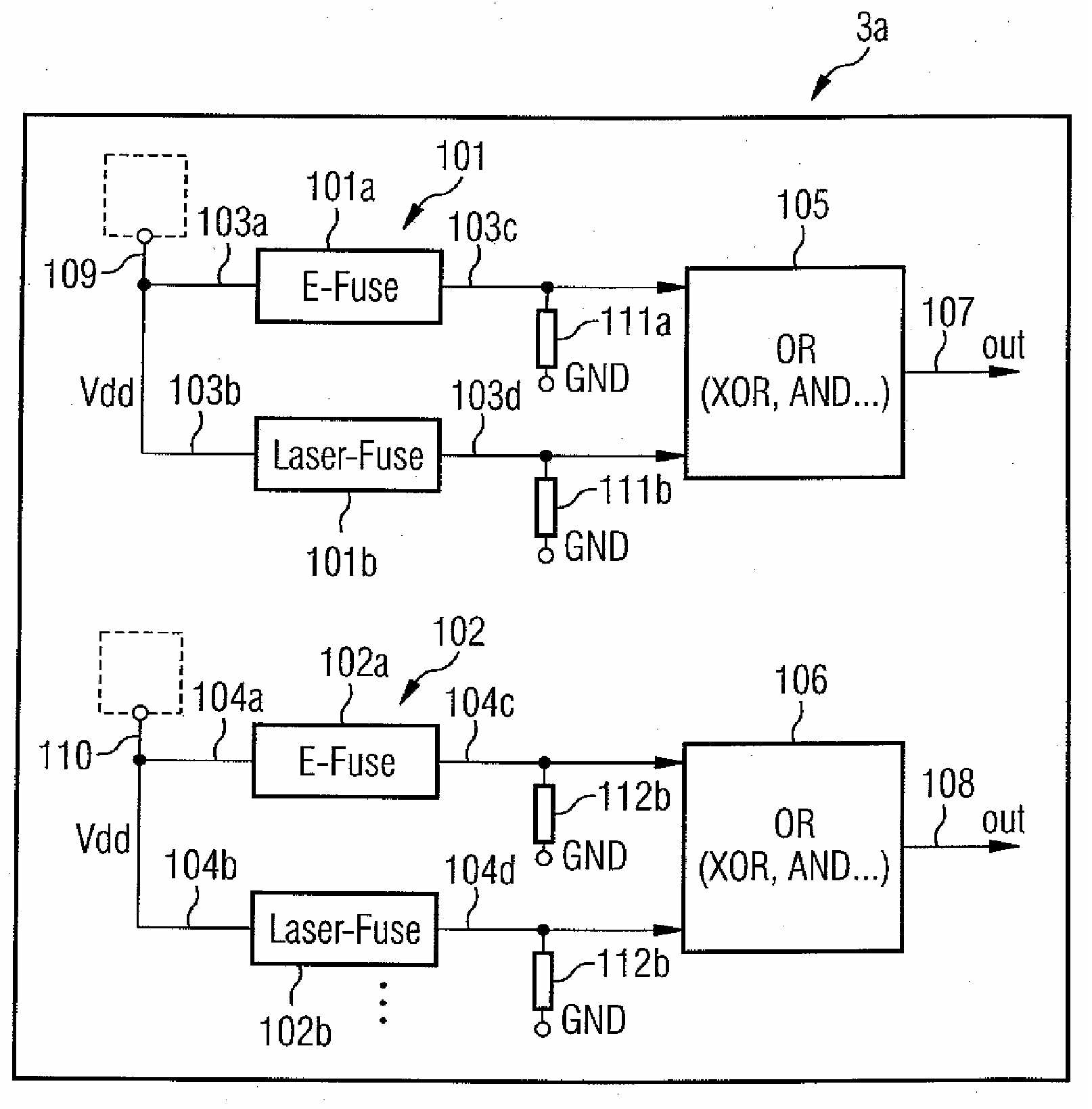
This place covers:
Fuse related issues; most of these documents have descriptions at transistor level, explaining how the fuse circuits are built or how they are included in the redundancy decoding elements.
This place covers:
In this case, a master fuse can be used to decide whether a redundant line or decoder is in use. This allows to save time when programming the fuses. See EP646866, fig.3 (reference 50).
Attention is drawn to the following places, which may be of interest for search:
Memories using fuses in general |
This place covers:
In these documents, the "fuse" is not a fuse as such, but rather a non-volatile memory cell or a combination of a fuse with a latch to retain its status (i.e. the fuse is only read at power up to reduce stress thereon). See US5619469, fig2.

Attention is drawn to the following places, which may be of interest for search:
Erasable programmable memory cells in general |
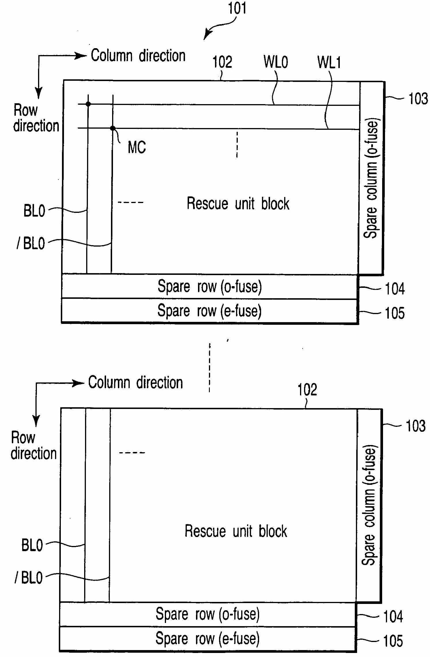
This place covers:
Under this group, techniques which tend to reduce real estate by several means. When the document is a pure layout description - i.e. without a clear functionality other than a "new layout" - it is included in this 'head group'. It should be clear that there is a clear "layout" approach in the description and figures.
This place covers:
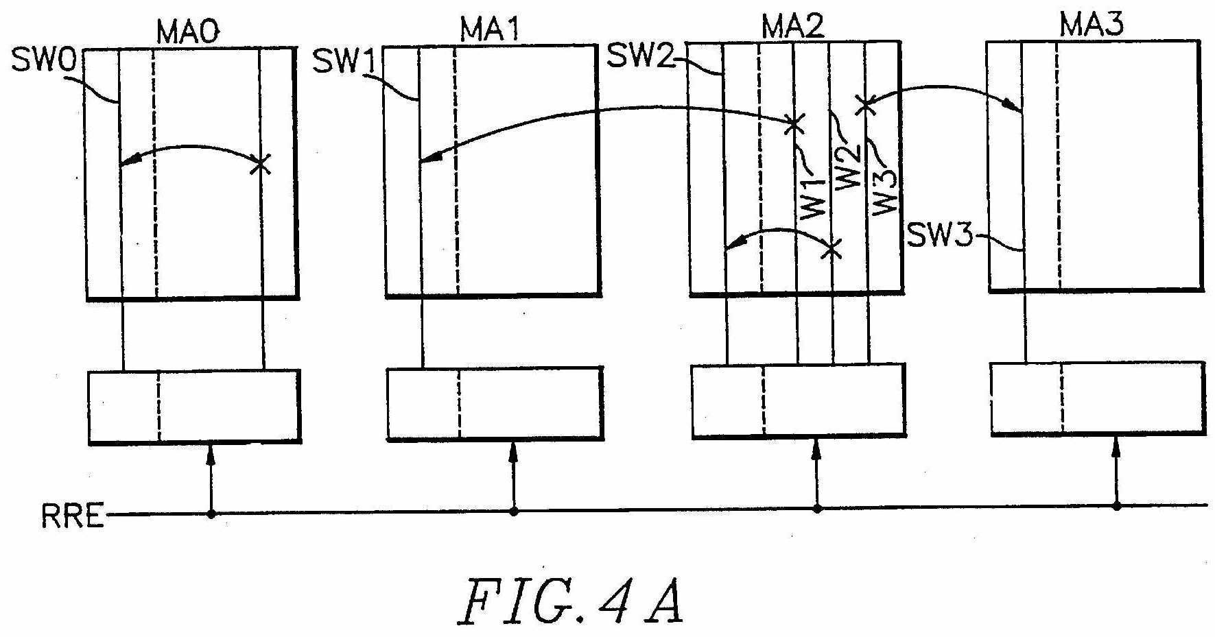
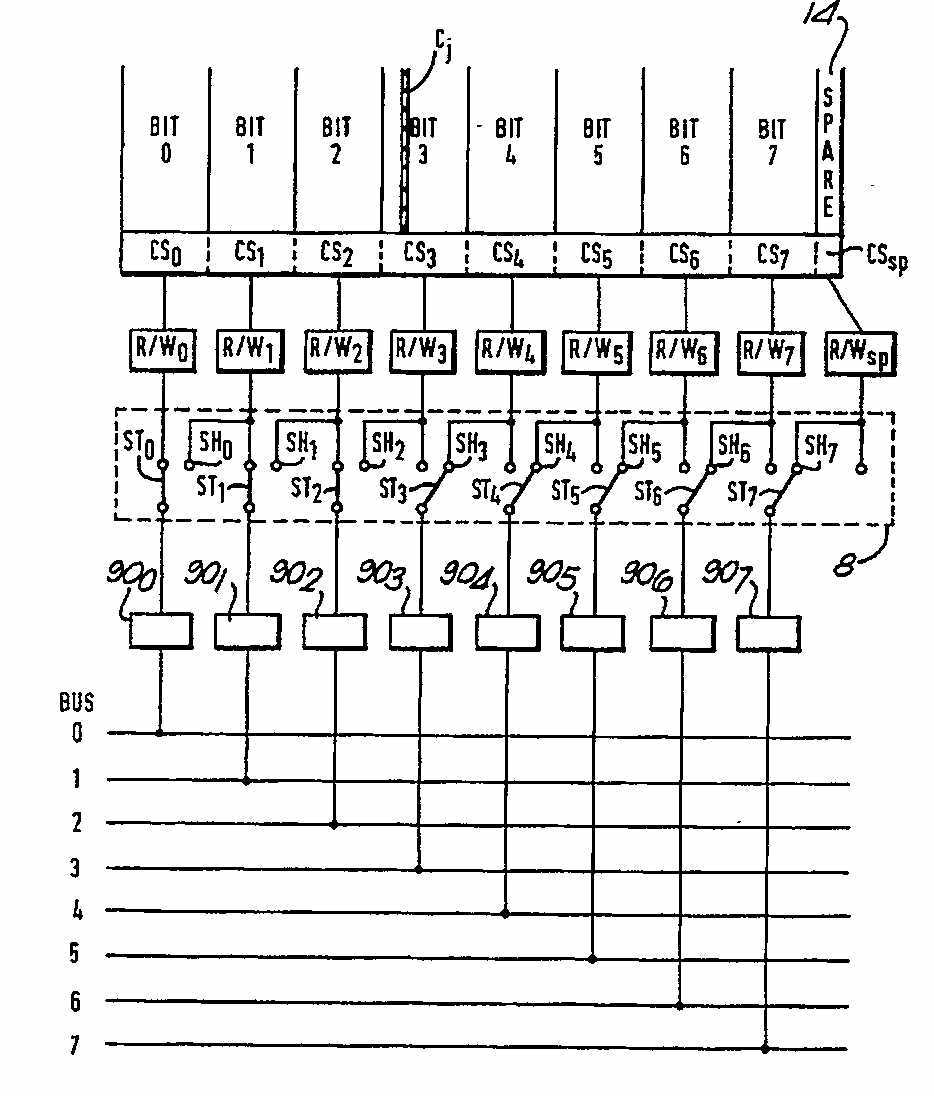
Transmission of faulty/redundant addresses between the fuse boxes and the final decoders is done by encoding: For 2n redundant lines only n lines have to be routed. See EP496282, fig.2.
This place covers:
Faults which involve several (adjacent) lines can be solved in a simplified way, 'simplified' implying using a reduced amount of coding or storage for the defect. These kind of faults are very frequent due to impurities of a big size. See US5281868, fig. 3,4.


This place covers:
Solutions that might have a lower redundancy efficiency (e.g. lines can only be replaced in sets of four, regardless of the fault) but allows to have fewer and/or smaller comparators. See EP239196, fig 3.
This place covers:
All kinds of solutions in which different combinations of faulty/redundant replacement are possible to allow for a higher level of repair with a lower number of spares. For instance, when redundant lines in a block can be used to substitute faulty lines in any other block, or when the same redundant line can be used for row or column repair, etc. See US5469388 fig 4A.
This place covers:
Faults are solved in a hierarchical way. For instance: lines are replaced with redundant lines in a given block or, if not possible, then the complete block is repaired with a redundant block as a whole unit, etc. See US5295101, fig. 7.

This place covers:
The amount of real estate occupied by fuses is lower.
This place covers:
The layout is done in such a way that a certain cost function associated with the yield is optimized. A lot of NPL and thesis-like stuff. See XP237814.
This place covers:
Certain applications (ROMs, synchronous memories, cache memories) demand redundancy solutions which are very related to the nature of the application itself and therefore more likely to be relevant in an application-oriented context.
This place covers:
For the case of Dual port RAMs, video memories and the like.
This place covers:
These redundancy solutions are usually taking into account the block erase operations as well as the aging of EEPROM cells due to program/erase. Many of these documents are also classified with the solid state disks solutions (G11C 29/765). Normally documents put in this group work at a lower level (i.e. row/columns in a block, rather than sector mapping level.
This place covers:
Redundancy solutions for Mask ROMs which have specific layouts.
This place covers:
Same as above for the case of synchronous memories. Timing (synchronicity) requirements as well as the specific (i.e. sequential) nature of read/write operations are linked to some redundancy requirements.
This place covers:
Most of the solutions for this problem are related to the avoidance of DC faults.
This place covers:
A common way to reduce power consumption in these cases.
This place covers:
Roll call circuits to identify redundancy substitutions.
This place covers:
Solving the problem of a faulty spare element which must be disabled for redundant substitution.
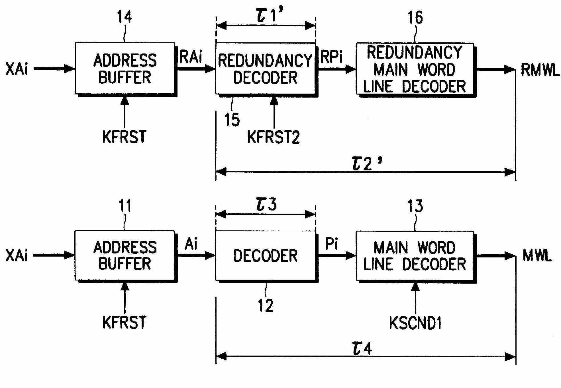
This place covers:
In this group, solutions which propose to eliminate or reduce the difference in speed between a non-faulty and a faulty line selection. Many of these documents are actually addressing stability problems (e.g. obtain a reliable voltage level before sampling fuse values) employing similar solutions such as ATDs.
This place covers:
The trick here usually is to insert a delay element in the faster path to make sure both paths (normal and redundant) are equally slow. This delay element usually consists of slower transistors in the path or a chain of inverters. See US5777931, fig.5.
This place covers:
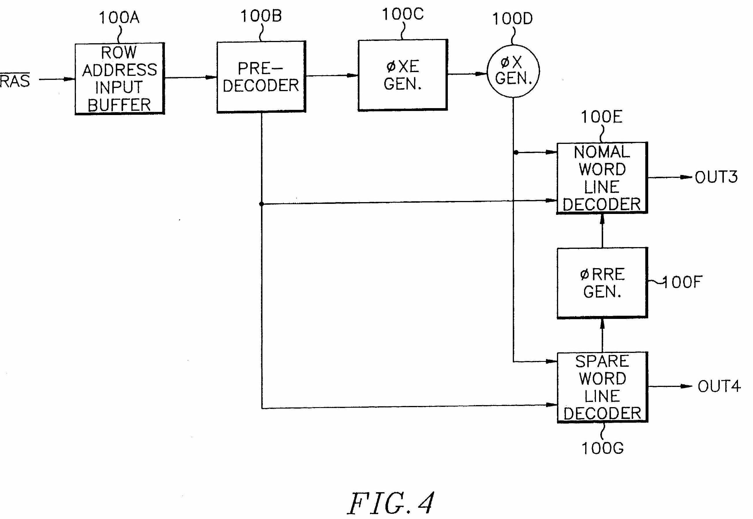
A normal/redundant selection signal is already obtained at a predecoding stage which allows to start some kind of preselection. See US5550776, fig.4.
This place covers:
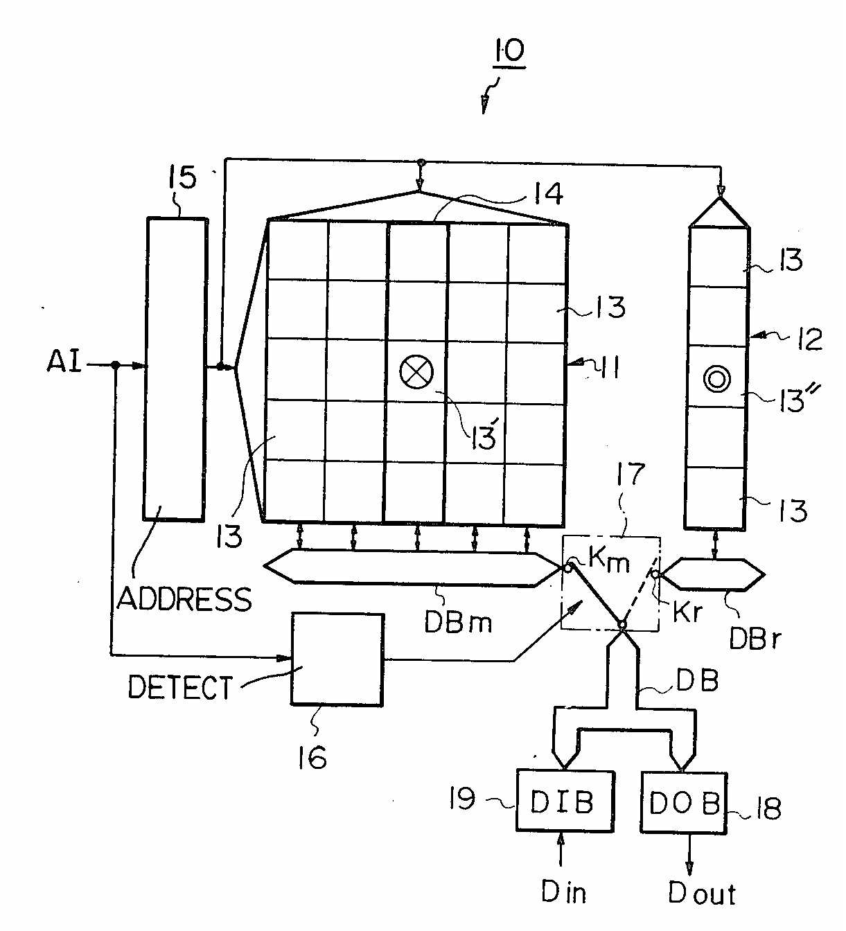
Usually the case with column redundancy: Addresses are input simultaneously to faulty and normal column decoders and only at the output (usually by means of a multiplexer) it is decided whether a redundant replacement is pertinent. See US4473895, fig.1.
This place covers:
Columns are shifted one or more position skipping the faulty one(s). There are redundant columns at the end of the chain. See EP434200, fig. 4.
This place covers:
Partially good memories, degraded memories.
In patent documents, the following abbreviations are often used:
DEP | Defective end product; (now G11C 29/883) |
CDEP | Combining defective end product. (now G11C 29/886) |
Attention is drawn to the following places, which may be of interest for search:
Attention is drawn to the following places, which may be of interest for search:
Input/output data interface arrangements for multiport memories each having random access ports and serial ports |
Attention is drawn to the following places, which may be of interest for search:
Sense amplifiers; Associated circuits |
Attention is drawn to the following places, which may be of interest for search:
Sense amplifiers; Associated circuits |
This place covers:
See US2006190762 (figure 1 - shown), US2009067276.
This place covers:
See US2008307251 (fig.1), US2009072886 (fig.1 - shown).
This place covers:
See US2008180983 (figure 2), US2006221729 (figure 3).