CPC Definition - Subclass H10K
This place covers:
Electric solid-state devices having organic materials as the active layers, or using a combination of organic materials and other materials as the active layers.
This includes the following kind of devices:
- organic devices specially adapted for rectifying, amplifying, oscillating or switching, or capacitors or resistors having potential barriers, e.g. organic transistors or organic diodes;
- organic devices that are sensitive to infrared radiation, light, electromagnetic radiation of shorter wavelength or corpuscular radiation, e.g. organic solar cells or organic photodiodes;
- organic light-emitting devices, e.g. organic light-emitting diodes or organic light-emitting transistors.
Processes and apparatus specially adapted for the manufacture or treatment of such devices.
Organic materials used in active layers, layers having high carrier mobility or electrodes of devices covered by this subclass.
This place does not cover:
Organic resistors without potential barriers and not being specially adapted for integrated devices | |
Organic capacitors, e.g. organic polymer capacitors, without potential barriers and not being specially adapted for integrated devices | |
Organic electronic memory devices | |
Organic thermoelectric devices; Organic thermomagnetic devices | |
Organic piezoelectric or electrostrictive devices | |
Organic magnetostrictive devices | |
Organic galvanomagnetic or Hall-effect devices | |
Organic superconducting devices | |
Organic solid-state devices without potential barriers, and specially adapted for rectifying, amplifying, oscillating or switching |
Examples of places in relation to which this place is residual:
Attention is drawn to the following places, which may be of interest for search:
Use of organic solid-state devices for measuring | |
Control arrangements or circuits for electroluminescent panels comprising organic light-emitting diodes [OLED] | |
Organic electromechanical resonators | |
Organic loudspeakers, microphones, gramophone pick-ups or like acoustic electromechanical transducers, e.g. organic piezoelectric microphones | |
Organic printed circuits, hybrid circuits, casings or constructional details thereof |
The scheme covers five main aspects: (a) devices, e.g. components, are covered by groups H10K 10/00, H10K 30/00 and H10K 50/00 (b) integrated devices and assemblies of multiple devices are covered by the groups H10K 19/00, H10K 39/00, H10K 59/00 and H10K 65/00, (c) processes and apparatus that are specially adapted for manufacturing or treating a device are covered in H10K 71/00, (d) constructional details that may be generic to the devices of the subclass are covered in H10K 77/00, (e) organic materials used in active layers, in layers having high carrier mobility, and in electrodes are covered in H10K 85/00.
Determination should be made as which of the five aspect(s) is/are inventive. Classification of the inventive aspect(s) should be made using inventive allocation in the appropriate part(s) of the scheme. Classification of the remaining aspects should then be made using additional allocation only if disclosed in specific embodiments, e.g. a concrete device embodiment, or a synthesis method.
In this subclass, the periodic system used is the I to VIII group system indicated in the Periodic Table under Note (3) of section C.
In this place, the following terms or expressions are used with the meaning indicated:
chip | a piece of a wafer or a substrate that has been processed to contain devices therein or thereon. The expression "diced chip" refers to the result of dicing a wafer or a substrate into a plurality of chips, whereas "undiced chip" refers to a chip before dicing or with no dicing. |
device | an electric circuit element (e.g. diode, transistor, LED, etc.); (depending on the context) can also refer to an integrated device (e.g. CMOS-IC, DRAM device, etc.). A device may be in the form of a bare or packaged chip. |
dopant | the atoms or compounds added to a material during doping |
doping | the intentional addition of a small quantity of atoms or compounds into a material to achieve a desired characteristic, e.g. to produce an n-type or p-type material |
individual | refers to: an electric circuit element not being an integrated device; or a component of an integrated device. Examples of individual devices include: diodes, transistors, photovoltaic cells, Josephson-junction devices, light-emitting diodes [LED], organic LEDs or a single LED component within an integrated device. |
integrated device | a device consisting of a plurality of semiconductor or other solid-state electric circuit elements formed in or on a common substrate |
integrated circuit | an integrated device where all the electric circuit elements (e.g. diodes, transistors, LEDs, etc.) are formed in or on a common substrate, including interconnections between the elements |
component | an electric circuit element (e.g. diode, transistor, LED, etc.) that is one of a plurality of elements formed in or on a common substrate, e.g. in an integrated device |
wafer | it can be one of the following: (a) a slice of semiconductor or electric solid-state active material. For example: a slice of silicon; a slice of a semiconducting compound, e.g. gallium nitride [GaN]; a slice of lithium tantalate [LiTaO3] for superconductor applications. (b) A multilayered laminate, having at least one layer of semiconductor or electric solid-state active material, the layer being meant to be processed into devices. For example: silicon-on-insulator [SOI]; silicon-on-glass [SOG]; silicon-on-sapphire [SOS]; a composite wafer comprising silicon carbide [SiC] on polycrystalline silicon [Si] support; a layer of semiconducting nanowires on glass. A wafer is typically processed by (e.g.) deposition, etching, doping or diffusion, and is then typically diced into chips. |
body | the region of semiconductor (resp. solid-state) material(s) within which, or at the surface of which, the physical effects that are characteristic of the device occur, and any bordering semiconductor (resp. solid-state) material(s) that are contiguous with this region. Examples: in a field-effect transistor [FET], the physical effects occur in the channel region between the source and the drain. The semiconductor body includes the channel region, the source and drain regions, and any contiguous semiconductor material; in a light-emitting diode [LED], the physical effects occur at a junction of active semiconductor layers. The semiconductor body includes these active semiconductor layers and any contiguous semiconductor layers, such as buffer layers, possibly a growth substrate, etc., that are between the cathode and anode electrodes; in a thermoelectric device, the solid-state body includes all solid-state materials in the path of current between the electrodes. |
electrode | a conductive region in or on the semiconductor body or solid-state body of a device (and other than the body itself) which exerts an electrical influence on the body, irrespective of whether or not an external electrical connection is made thereto. The term covers metallic regions which exert electrical influence on the body through an insulating region (e.g. in intentional non-parasitic capacitive coupling), or inductive coupling arrangements. In a capacitive coupling arrangement, the dielectric region is regarded as part of the electrode. The overall conductive wiring may comprise multiple portions. In such a case, only the wiring portions that exert an electrical influence on the body are considered portions of the electrode. Examples: conductive layer(s) in direct physical contact with the body; conductive region(s) exerting an inductive coupling onto the body; a multilayer structure which exerts influence on the body through an insulating region, e.g. in intentional non-parasitic capacitive coupling. |
interconnection | a conductive arrangement for conducting electric current from an electrode of a circuit element to another part of the circuit. Examples include metal wirings. |
container | a solid construction in which (one or more) devices are placed, or which is formed around the devices, for forming packaged devices. A container requires a partial or total enclosure and it may also comprise a filling. |
encapsulation | an enclosure consisting of (one or more) layers, e.g. comprising organic polymers, which at least partially enclose the (one or more) devices, thereby protecting them. An encapsulation is often used to hermetically seal devices. |
field-effect | refers to semiconductor technology wherein a voltage applied to a gate electrode creates an electric field that allows for control of current near the interface of the gate and the body, e.g. to create an inversion channel between the source and drain of a MOSFET |
package | the collection of all elements, which are external to the chip, that protect the chip or connect it to another object. Package therefore covers encapsulations, containers, package substrates, interposers, heatsinks or the like. Package does not include objects at a higher system level, like circuit boards and beyond, e.g. a housing in which the circuit board is enclosed. |
unipolar | refers to semiconductor technology that primarily involves one type only of charge carrier, i.e. it involves either holes or electrons but not both |
bipolar | refers to semiconductor technology that involves multi-carrier-type operation, i.e. which simultaneously uses both electrons and holes as charge carriers |
MIS | metal-insulator-semiconductor |
MOS | metal-oxide-semiconductor |
FET | field-effect transistor |
MISFET | metal-insulator-semiconductor field-effect transistor |
TFT | thin-film transistor |
active material | the material within which the physical effects that are characteristic of the device occur |
auxiliary electrode | one part of a multi-layered electrode, often being metallic and intended to increase the conductivity of transparent oxide electrodes |
coordination compound | a material having a chemical structure in which a central atom is chemically bonded to surrounding nonmetal atoms or groups of atoms. The central atom may be a metal atom or may be a metalloid (e.g. B, Si, Ge, As, Sb, Te or Po). |
electroluminescent layer, emissive layer | the layer within which electrons and holes combine, resulting in light emission |
organic device | a device that comprises one or more organic materials as the active material, e.g. using only organic active materials or e.g. using a combination of an organic material and another material |
radiation-sensitive | refers to a device or a component that is sensitive to infrared radiation, light, electromagnetic radiation of shorter wavelength or corpuscular radiation |
tandem OLED | an OLED that comprises multiple electroluminescent units between one set of electrodes and a charge generation layer between the electroluminescent units |
tandem PV cell | a photovoltaic cell that comprises multiple stacked photovoltaic units, e.g. p-n junctions, between one set of electrodes. Often each unit is made from a semiconductor of different bandgap energy, so each is sensitive to a different part of the electromagnetic spectrum. |
terminal | the electrode or interconnection within a device, which serves as a connecting point between electrodes or interconnections within the device and interconnections that may be in the device's package or may be external to the device. An example is a bond pad on the cathode of an OLED, which may connect between the cathode electrode and a bonding wire in the OLED's package. |
tiled display | a display that comprises a juxtaposition of smaller interconnected panels in order to achieve a large-area display |
In patent documents, the following abbreviations are often used:
CCM | Colour changing material |
EBL | Electron blocking layer |
EIL | Electron injection layer |
EL | Electroluminescent; or electroluminescent layer |
ETL | Electron transporting layer |
FTO | Fluorine doped tin oxide |
HBL | Hole blocking layer |
HIL | Hole injection layer |
HOIP | Hybrid organic-inorganic perovskite |
HOMO | Highest occupied molecular orbital |
HTL | Hole transporting layer |
ITO | Indium tin oxide |
LEC | Light-emitting electrochemical cell |
LUMO | Lowest unoccupied molecular orbital |
OEL | Organic electroluminescent layer |
OLED | Organic light-emitting diode |
OTFT | Organic thin-film transistor |
PLED | Polymer light-emitting diode |
RGB | Red Green Blue |
RGBW | Red Green Blue White |
TCO | Transparent conductive oxide |
This place covers:
Organic devices wherein an electrical input is rectified, amplified, oscillated or switched.
Active resistors or capacitors using organic materials as the active layers, or using a combination of organic materials with other material as the active layers.
Examples include:
- Organic variable resistors;
- Organic variable capacitors;
- Organic diodes;
- Organic transistors.
This place does not cover:
Organic integrated devices, or assemblies of multiple devices |
Attention is drawn to the following places, which may be of interest for search:
Manufacture or treatment specially adapted for organic devices | |
Constructional details generally applicable to all organic solid-state devices, not covered by this group | |
Organic material used in active layers, in layers having high carrier mobility or in electrodes | |
Individual inorganic semiconductor devices specially adapted for rectifying, amplifying, oscillating or switching; Individual inorganic resistors or capacitors having potential barriers; Individual resistors, capacitors or inductors having no potential barriers, and specially adapted for integration with other semiconductor components |
Attention is drawn to the following places, which may be of interest for search:
Organic light-sensitive diodes | |
Organic light-emitting diodes |
This place does not cover:
Bipolar transistors, e.g. organic bipolar junction transistors [OBJTs] |
Examples of places where the subject matter of this place is covered when specially adapted, used for a particular purpose, or incorporated in a larger system:
CHEMFETs |
Attention is drawn to the following places, which may be of interest for search:
Organic light-sensitive transistors | |
Organic light-emitting transistors | |
Organic thin film transistors in an organic light-emitting display |
This place covers:
Integrated devices comprising at least one organic component specially adapted for rectifying, amplifying, oscillating or switching covered by group H10K 10/00.
Assemblies of multiple devices comprising at least one organic device specially adapted for rectifying, amplifying, oscillating or switching covered by group H10K 10/00.
Attention is drawn to the following places, which may be of interest for search:
Individual organic devices specially adapted for rectifying, amplifying, oscillating or switching | |
Organic light-emitting display comprising organic thin film transistors | |
Manufacture or treatment specially adapted for organic devices | |
Constructional details generally applicable to all organic solid-state devices, not covered by this group | |
Integrated devices comprising inorganic components specially adapted for rectifying, amplifying, oscillating or switching |
This place covers:
Devices specially adapted for sensing infra-red radiation, light, electro-magnetic radiation of shorter wavelength or corpuscular radiation and adapted for the conversion of the energy of such radiation into electrical energy or for the control of electrical energy by such radiation using organic materials as the active layers, or using a combination of organic materials with other material as the active layers.
Examples include:
- Organic solar cells
- Organic photodiodes
- Organic phototransistors
- Organic photoresistors or photoconductors
H10K 30/50 - H10K 30/57 specifically cover photovoltaic cells. H10K 30/60 - H10K 30/65 specifically cover photodiodes, photoresistors and phototransistors. H10K 30/10 - H10K 30/451 cover structural or junction aspects of photovoltaic cells, photodiodes, photoresistors and phototransistors.
This place does not cover:
Organic integrated devices, or assemblies of multiple devices | |
Electrolytic light-sensitive devices |
Attention is drawn to the following places, which may be of interest for search:
Organic light-emitting devices | |
Manufacture or treatment specially adapted for organic devices | |
Constructional details generally applicable to all organic solid-state devices, not covered by this group | |
Organic material used in active layers, in layers having high carrier mobility, or in electrodes | |
Inorganic radiation-sensitive devices |
This place covers:
- Integrated devices comprising at least one component specially adapted for sensing infra-red radiation, light, electro-magnetic radiation of shorter wavelength or corpuscular radiation and adapted for the conversion of the energy of such radiation into electrical energy or for the control of electrical energy by such radiation using organic materials as the active layers, or using a combination of organic materials with other material as the active layers; and
- Assemblies of multiple devices, comprising at least one device specially adapted for sensing infra-red radiation, light, electro-magnetic radiation of shorter wavelength or corpuscular radiation and adapted for the conversion of the energy of such radiation into electrical energy or for the control of electrical energy by such radiation using organic materials as the active layers, or using a combination of organic materials with other material as the active layers.
Such as:
- Integrated devices comprising organic solar cells
- Organic photovoltaic modules
- Organic image sensors (imager structures)
- Organic X-ray detectors
Attention is drawn to the following places, which may be of interest for search:
Integrated devices, e.g. driving circuitry, comprising organic components specially adapted for rectifying, amplifying, oscillating or switching | |
Individual organic radiation-sensitive components of these integrated devices | |
Organic optocouplers | |
Manufacture or treatment specially adapted for organic devices | |
Constructional details generally applicable to all organic solid-state devices, not covered by this group | |
Integrated devices, e.g. driving circuitry, comprising inorganic components specially adapted for rectifying, amplifying, oscillating or switching | |
Integrated devices comprising inorganic radiation-sensitive components |
This place covers:
Organic electrical-light transducers wherein an electrical input is converted to a light output, such as organic light-emitting diodes [OLED] or organic light-emitting transistors.
This place does not cover:
Organic integrated devices, or assemblies of multiple devices | |
Organic semiconductor lasers |
Examples of places where the subject matter of this place is covered when specially adapted, used for a particular purpose, or incorporated in a larger system:
Lighting devices for vehicle interior | |
Light sources using semiconductor devices as light-generating elements, e.g. using light-emitting diodes [LED] or lasers | |
Lighting devices intended for fixed installation | |
Illumination devices for LCDs | |
Indicating arrangements making use of semiconductor devices | |
Illuminated signs |
Attention is drawn to the following places, which may be of interest for search:
Manufacture or treatment specially adapted for organic devices | |
Constructional details generally applicable to all organic solid-state devices, not covered by this group | |
Organic material used in active layers, in layers having high carrier mobility or in electrodes | |
Luminescent or electroluminescent materials | |
Light sources using luminescence, e.g. lamps based on OLEDs | |
Details of lighting devices, of general application | |
Control arrangements or circuits, of interest only in connection with visual indicators other than cathode-ray tubes, e.g. control arrangements for OLED displays | |
Electroluminescent light sources | |
Inorganic light-emitting diodes |
In patent documents, the following abbreviations are often used:
EL | Electroluminescent, electroluminescent layer |
OEL | Organic electroluminescent layer |
EIL | Electron injection layer |
HIL | Hole injection layer |
ETL | Electron transporting layer |
HTL | Hole transporting layer |
EBL | Electron blocking layer |
HBL | Hole blocking layer |
LEC | Light-emitting electrochemical cells |
OLED | Organic light-emitting diode |
TOLED | Transparent OLED |
AMOLED display | Active matrix OLED display |
PMOLED display | Passive matrix OLED display |
OTFT | Organic thin film transistor |
TFT | Thin film transistor |
CCM | Colour changing medium |
RGB | Red Green Blue |
RGBW | Red Green Blue White |
This place covers:
Integrated devices that comprise at least one organic light-emitting component;
Assemblies of multiple devices, comprising at least one organic light-emitting device.
Examples include:
- Arrays of organic light-emitting diodes [OLEDs], e.g. OLED display
- An OLED integrated with a MOSFET
H10K 59/10 covers only OLED displays, whereas H10K 59/30 - H10K 59/90 cover both displays and non-displays.
Examples of places where the subject matter of this place is covered when specially adapted, used for a particular purpose, or incorporated in a larger system:
Lighting devices for vehicle interior | |
Light sources using semiconductor devices as light-generating elements, e.g. using light-emitting diodes [LED] or lasers | |
Lighting devices intended for fixed installation | |
Illumination devices, e.g. backlights, for LCDs | |
Indicating arrangements making use of semiconductor devices | |
Illuminated signs |
Attention is drawn to the following places, which may be of interest for search:
Individual organic light-emitting components of these integrated devices | |
Integrated devices comprising at least one organic light-emitting component and at least one organic radiation-sensitive component, e.g. organic opto-couplers | |
Manufacture or treatment specially adapted for organic devices | |
Constructional details generally applicable to all organic solid-state devices, not covered by this group | |
Luminescent, e.g. electroluminescent materials | |
Light sources using luminescence, e.g. lamps based on OLEDs | |
Details of lighting devices, of general application | |
Liquid crystal displays [LCD] | |
Control arrangements or circuits, of interest only in connection with visual indicators other than cathode-ray tubes, e.g. control arrangements for OLED displays | |
Plasma displays | |
Field emission displays | |
Electroluminescent light sources | |
Circuit arrangements for operating LEDs comprising organic material | |
Integrated devices comprising inorganic light-emitting components, e.g. LED displays |
In this place, the following terms or expressions are used with the meaning indicated:
OLED display | Organic light emitting diode display |
TOLED display | Transparent OLED display |
AMOLED display | Active matrix OLED display |
PMOLED display | Passive matrix OLED display |
OTFT array | Organic thin film transistor array |
TFT array | Thin film transistor array |
CCM | Colour changing medium |
RGB | Red Green Blue |
RGBW | Red Green Blue White |
H10K 59/10 covers only OLED displays. H10K 59/30 - H10K 59/90 cover displays, non-display integrated devices and non-display assemblies of multiple devices.
Attention is drawn to the following places, which may be of interest for search:
Control arrangements for OLED displays | |
TFT arrays, per se |
This place covers:
Integrated devices comprising at least one organic light-emitting component and at least one organic radiation-sensitive component, e.g. organic optocouplers;
Assemblies of multiple devices, comprising at least one organic light-emitting device and at least one organic radiation-sensitive device, e.g. organic optocouplers
Example:
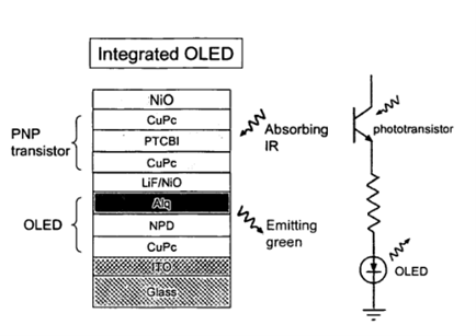
The example shows a combination of an organic phototransistor with an OLED.
This place does not cover:
Organic image sensors integrated with organic light-emitting diodes | |
OLED displays integrated with photosensors |
Attention is drawn to the following places, which may be of interest for search:
Individual organic radiation-sensitive components of these integrated devices | |
Individual organic light-emitting components of these integrated devices | |
Manufacture or treatment specially adapted for organic devices | |
Constructional details generally applicable to all organic solid-state devices, not covered by this group | |
Inorganic optocouplers |
This place covers:
Processes or apparatus specially adapted for the formation of organic solid-state devices, including the formation, patterning or treatment of the organic materials used in active layers, in layers having high carrier mobility or in electrodes of an organic solid-state device.
Attention is drawn to the following places, which may be of interest for search:
Spraying apparatus | |
Processes for applying liquids or other fluent materials | |
Ink jet printers | |
Printing processes to produce particular kinds of printed work | |
Surface treatment of glass substrates by at least two coatings | |
Joining glass to inorganic material or glass | |
Etching, surface-brightening or pickling compositions | |
Coating by vacuum evaporation, sputtering or by ion implantation of the coating forming material | |
Chemical coating by decomposition of gaseous compounds | |
Photomechanical, e.g. photolithographic, production of textured or patterned surfaces | |
Manufacture or treatment for semiconductor devices |
This place covers:
This place covers details that are generic or generally applicable to all device types of H10K, e.g. transparent or flexible substrates.
Attention is drawn to the following places, which may be of interest for search:
Constructional details specific to organic devices specially adapted for rectifying, amplifying, oscillating or switching, or organic capacitors or resistors having potential barriers | |
Constructional details specific to organic radiation-sensitive devices | |
Constructional details specific to organic light-emitting devices | |
Conductors or conductive bodies characterised by the conductive materials | |
Insulators or insulating bodies characterised by the insulating materials |
This place covers:
Organic materials in devices of this subclass, selected for their electrical or other properties, and used in
- Active layers, e.g. channel layers or light-emitting layers
- Layers having high carrier mobility, e.g. electron or hole transport layers
- Electrodes
Attention is drawn to the following places, which may be of interest for search:
Carbon; Compounds thereof, e.g. Fullerenes | |
Cyclic hydrocarbons containing rings other than, or in addition to, six-membered aromatic rings | |
Cyclic hydrocarbons containing only six-membered aromatic rings as cyclic parts | |
Ketones; Ketenes | |
Quinones | |
Compounds containing amino groups bound to a carbon skeleton | |
Heterocyclic compounds | |
Macromolecular compounds obtained by reactions forming a carbon-to-carbon link in the main chain of the macromolecule | |
Macromolecular compounds obtained by reactions forming a linkage containing nitrogen with or without oxygen or carbon in the main chain of the macromolecule | |
Dyes with anthracene nucleus not condensed with any other ring | |
Dyes with an anthracene nucleus condensed with one or more carbocyclic rings | |
Dyes with an anthracene nucleus condensed with one or more heterocyclic rings with or without carbocyclic rings | |
Acridine dyes | |
Methine or polymethine dyes, e.g. cyanine dyes | |
Porphines; Azaporphines | |
Quinacridones | |
Dyes of natural origin prepared from natural sources, e.g. vegetable sources | |
Luminescent, e.g. electroluminescent, chemoluminescent materials | |
Etching, surface-brightening or pickling compositions | |
Liquid crystal materials | |
Organic conductors, in general | |
Organic insulators, in general |
Special rules for classifying chemical compounds:
Markush formulae or generic formulae are not classified, only concrete embodiments or examples are classified. Simple lists of known compounds (without application in an example or embodiment) are not classified.
Fullerenes and carbon nanotubes are considered to be organic material. Graphene is considered to be inorganic.
In addition to the polymer classification, H10K 85/10, the side-chains of aromatic or aliphatic polymers may be classified in the appropriate subgroup (e.g. H10K 85/30, H10K 85/40, H10K 85/50, H10K 85/60).
Aromatic or aliphatic polymers comprising a metal complex in their main chain are classified in both H10K 85/10 and in H10K 85/30.
Silicon containing compounds are classified in H10K 85/40 and are additionally classified in in H10K 85/10, H10K 85/20, H10K 85/30, H10K 85/50 and/or H10K 85/60 as appropriate.
Ligands of metal complexes are not additionally classified in H10K 85/60.