CPC Definition - Subclass H10B
This place covers:
Memory devices consisting of multiple semiconductor or solid-state components. This includes the multiple memory cells constituting the memory core region and logic components within the immediate peripheral region surrounding the memory core region. The memory cells have storage components therein, which may be accessed by selection components.
This includes the following kind of devices:
Volatile Memory Devices:
- Static random access memory
- Dynamic random access memory
Non-Volatile Memory Devices:
- Read-only memory [ROM]
- Programmable ROM [PROM]
- Erasable and programmable ROM [EPROM]
- Electrically erasable and programmable ROM [EEPROM]
- Ferroelectric memory, e.g. FeRAM or FeFET
- Magnetic random access memory [MRAM]
- Resistive random access memory [ReRAM or RRAM], phase change RAM [PRAM or PCRAM]
Assemblies of multiple devices comprising at least one memory device of this subclass.
Processes and apparatus specially adapted for the manufacture or treatment of such devices.
Attention is drawn to the following places, which may be of interest for search:
Circuits (e.g. data buffers, decoders, sense amplifiers) and accessing (e.g. read, write, and erase operations) of memory devices |
In this place, the following terms or expressions are used with the meaning indicated:
chip | a piece of a wafer or a substrate that has been processed to contain devices therein or thereon. The expression "diced chip" refers to the result of dicing a wafer or a substrate into a plurality of chips, whereas "undiced chip" refers to a chip before dicing or with no dicing. |
device | an electric circuit element (e.g. diode, transistor, LED, etc.); (depending on the context) can also refer to an integrated device (e.g. CMOS-IC, DRAM device, etc.). A device may be in the form of a bare or packaged chip. |
dopant | the atoms or compounds added to a material during doping |
doping | the intentional addition of a small quantity of atoms or compounds into a material to achieve a desired characteristic, e.g. to produce an n-type or p-type material |
individual | refers to: an electric circuit element not being an integrated device; or a component of an integrated device. Examples of individual devices include: diodes, transistors, photovoltaic cells, Josephson-junction devices, light-emitting diodes [LED], organic LEDs or a single LED component within an integrated device. |
integrated device | a device consisting of a plurality of semiconductor or other solid-state electric circuit elements formed in or on a common substrate |
integrated circuit | an integrated device where all the electric circuit elements (e.g. diodes, transistors, LEDs, etc.) are formed in or on a common substrate, including interconnections between the elements |
component | an electric circuit element (e.g. diode, transistor, LED, etc.) that is one of a plurality of elements formed in or on a common substrate, e.g. in an integrated device |
wafer | it can be one of the following: (a) a slice of semiconductor or electric solid-state active material. For example: a slice of silicon; a slice of a semiconducting compound, e.g. gallium nitride [GaN]; a slice of lithium tantalate [LiTaO3] for superconductor applications. (b) A multilayered laminate, having at least one layer of semiconductor or electric solid-state active material, the layer being meant to be processed into devices. For example: silicon-on-insulator [SOI]; silicon-on-glass [SOG]; silicon-on-sapphire [SOS]; a composite wafer comprising silicon carbide [SiC] on polycrystalline silicon [Si] support; a layer of semiconducting nanowires on glass. A wafer is typically processed by (e.g.) deposition, etching, doping or diffusion, and is then typically diced into chips. |
body | the region of semiconductor (resp. solid-state) material(s) within which, or at the surface of which, the physical effects that are characteristic of the device occur, and any bordering semiconductor (resp. solid-state) material(s) that are contiguous with this region. Examples: in a field-effect transistor [FET], the physical effects occur in the channel region between the source and the drain. The semiconductor body includes the channel region, the source and drain regions, and any contiguous semiconductor material; in a light-emitting diode [LED], the physical effects occur at a junction of active semiconductor layers. The semiconductor body includes these active semiconductor layers and any contiguous semiconductor layers, such as buffer layers, possibly a growth substrate, etc., that are between the cathode and anode electrodes; in a thermoelectric device, the solid-state body includes all solid-state materials in the path of current between the electrodes. |
electrode | a conductive region in or on the semiconductor body or solid-state body of a device (and other than the body itself) which exerts an electrical influence on the body, irrespective of whether or not an external electrical connection is made thereto. The term covers metallic regions which exert electrical influence on the body through an insulating region (e.g. in intentional non-parasitic capacitive coupling), or inductive coupling arrangements. In a capacitive coupling arrangement, the dielectric region is regarded as part of the electrode. The overall conductive wiring may comprise multiple portions. In such a case, only the wiring portions that exert an electrical influence on the body are considered portions of the electrode. Examples: conductive layer(s) in direct physical contact with the body; conductive region(s) exerting an inductive coupling onto the body; a multilayer structure which exerts influence on the body through an insulating region, e.g. in intentional non-parasitic capacitive coupling. |
interconnection | a conductive arrangement for conducting electric current from an electrode of a circuit element to another part of the circuit. Examples include metal wirings. |
container | a solid construction in which (one or more) devices are placed, or which is formed around the devices, for forming packaged devices. A container requires a partial or total enclosure and it may also comprise a filling. |
encapsulation | an enclosure consisting of (one or more) layers, e.g. comprising organic polymers, which at least partially enclose the (one or more) devices, thereby protecting them. An encapsulation is often used to hermetically seal devices. |
field-effect | refers to semiconductor technology wherein a voltage applied to a gate electrode creates an electric field that allows for control of current near the interface of the gate and the body, e.g. to create an inversion channel between the source and drain of a MOSFET |
package | the collection of all elements, which are external to the chip, that protect the chip or connect it to another object. Package therefore covers encapsulations, containers, package substrates, interposers, heatsinks or the like. Package does not include objects at a higher system level, like circuit boards and beyond, e.g. a housing in which the circuit board is enclosed. |
unipolar | refers to semiconductor technology that primarily involves one type only of charge carrier, i.e. it involves either holes or electrons but not both |
bipolar | refers to semiconductor technology that involves multi-carrier-type operation, i.e. which simultaneously uses both electrons and holes as charge carriers |
MIS | metal-insulator-semiconductor |
MOS | metal-oxide-semiconductor |
FET | field-effect transistor |
MISFET | metal-insulator-semiconductor field-effect transistor |
TFT | thin-film transistor |
programming | setting a desired state of a memory cell |
writing, erasing | changing the state of a memory cell, in a memory cell wherein programming can occur as many times as desired |
core, core region | the portion of a memory cell having storage components, select components, or data lines such as bit lines and word lines. The core also includes devices for local accessing (e.g. reading, writing or erasing) of the storage elements, for example, select transistors of NAND strings or read/write ports of SRAM. |
peripheral region, periphery | the portion of a memory device outside the core region having devices or parts for global accessing (e.g. reading, writing, erasing) of the devices of the core region. It includes, e.g. word line drivers, multiplexers or sense amplifiers. |
boundary region between the core region and peripheral circuit region | the portion of a memory device that contains neither core devices (e.g. storage components or select components) nor peripheral devices (e.g. word line drivers or multiplexers), typically comprising structural parts such as bit line fan-outs between the core region and the peripheral region, or dummy elements or staircase structures for 3D NAND |
In patent documents, the following abbreviations are often used:
RAM | Random access memory |
SRAM | Static RAM |
DRAM | Dynamic RAM |
ReRAM, RRAM | Resistive RAM |
PRAM, PCRAM | Phase change RAM |
FeRAM, FRAM | Ferroelectric RAM |
CBRAM | Conductive-bridging RAM |
MRAM | Magnetoresistive RAM |
ROM | Read-only memory |
PROM | Programmable ROM |
MPROM | Mask-programmed ROM |
OTPROM | One-time programmable ROM |
EPROM | Erasable-and-programmable ROM |
Volatile memory | Memory requiring power supply to maintain the stored information: it loses any written data when the system is turned off |
Non-volatile memory | Memory not requiring power supply to maintain the stored information: it retains the written data even when the system is turned off |
Ferroelectric memory capacitor | Capacitor with ferroelectric memory properties |
Ferroelectric memory transistor | Transistor with ferroelectric memory properties embedded in a layer of the gate electrodes, e.g. in a MFS or MFMIS layer |
MFS | Metal-ferroelectric-semiconductor |
MFIS | Metal-ferroelectric-insulator-semiconductor |
MFMIS | Metal-ferroelectric-metal-insulator-semiconductor |
This place covers:
Memory devices having multiple volatile memory cells, wherein, in each cell, the logic state is stored in one of two stable states of a cross-coupled inverter. SRAM cells commonly have four or more transistors.
Attention is drawn to the following places, which may be of interest for search:
Circuits (e.g. data buffers, decoders, amplifiers) and accessing (e.g. read, write and erase operations) of SRAM devices | |
Resistors for integrated circuits, and manufacturing or treatment thereof |
In patent documents, the following words/expressions are often used with the meaning indicated:
Vcc or Vdd | High voltage supply |
Vss | Low voltage (or ground) supply |
Pull-up [PU]/Load | Refers to components in the flip-flop that are connected to Vcc |
Pull-down [PD]/Drive | Refers to components in the flip-flop that are connected to Vss |
Pass-gate [PG], access transistor/gate, select transistor/gate, transfer transistor/gate | Refers to transistors that control access to the flip-flop |
Cross-coupled inverter (or Flip-flop or latch) | Bi-stable circuit used to store information |
This place covers:
Dynamic memory devices having multiple volatile memory cells, wherein, each cell has:
- a storage component (e.g. capacitor) whose stored charge determines the logic state of the device; and
- at least one selection component (e.g. access transistor) for accessing the storage component.
Attention is drawn to the following places, which may be of interest for search:
Circuits (e.g. data buffers, decoders, amplifiers) and accessing (e.g. read, write and erase operations) of DRAM devices | |
Capacitors for integrated circuits, and manufacture or treatment thereof |
This place covers:
Memory devices wherein data is stored even when power is removed (non-volatile), wherein the cells have components (e.g. fuses or anti-fuses) that are irreversibly changed during programming.
The group H10B 20/00 itself covers memory devices wherein, after manufacturing, the operations are limited to read-only (e.g. mask ROM), because the programming thereof was performed during manufacturing. The groups H10B 20/20 - H10B 20/25 cover programmable ROM [PROM] wherein the memory may be programmed after manufacturing by a user.
ROM and PROM devices are typically programmable only once (though in some situations, a cell may have more than one element that may be irreversibly changed, so a very limited amount of "corrective" programming may occur). This is contrasted with EPROM and EEPROM devices, which can be writable or erasable many (e.g. millions of) times.
Attention is drawn to the following places, which may be of interest for search:
Circuits (e.g. data buffers, decoders, amplifiers) and accessing (e.g. read, write and erase operations) of ROM devices |
This place covers:
Non-volatile ROM devices comprising multiple memory cells that can be programmed after their manufacture ("programmable ROM" or "PROM"), wherein the memory cell comprises field-effect components as either the access component or the storage component.
The group H10B 20/20 itself covers PROM wherein individual memory cells may each be programmed more than once, e.g. a "corrective programming" may occur because the cells have more than one element that may be irreversibly-changeable element. The groups indented under H10B 20/20 cover PROM wherein each cell may only be programmed once.
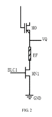
Illustrative example for this group: a cell is constructed from an anti-fuse programming transistor M0, an electronic fuse EF, and a control transistor MN1, such that the normal programming of M0 by breaking down its gate-source insulation layer (which decreases its initial large resistance) can be followed by "correction programming" by fusing the effuse (increasing the resistance).
This place does not cover:
ROM devices comprising bipolar components |
Attention is drawn to the following places, which may be of interest for search:
Circuits (e.g. data buffers, decoders, amplifiers) and accessing (e.g. read, write and erase operations) of ROM devices | |
Anti-fuses, i.e. connections having their state changed from non-conductive to conductive | |
Fuses, i.e. connections having their state changed from conductive to non-conductive |
This place covers:
Non-volatile programmable ROM (PROM) devices comprising multiple memory cells wherein, after their manufacture, each cell can only be programmed once (e.g. by permanently connecting or disconnecting a fuse or an anti-fuse).
Attention is drawn to the following places, which may be of interest for search:
Circuits (e.g. data buffers, decoders, amplifiers) and accessing (e.g. read, write and erase operations) of one-time PROM devices |
This place covers:
Non-volatile memory devices having multiple memory cells, wherein in each cell, the logic state is stored as charge on a floating gate of a transistor. The memory cell can be electrically erased and reprogrammed.
Attention is drawn to the following places, which may be of interest for search:
EEPROM devices comprising charge-trapping gate insulators | |
Ferroelectric memory devices comprising ferroelectric memory transistors | |
Circuits (e.g. data buffers, decoders, amplifiers) and accessing (e.g. read, write and erase operations) of EEPROM devices | |
Floating-gate transistors per se | |
Gate electrodes comprising a conductor-insulator-conductor-insulator-semiconductor structure |
This place covers:
Non-volatile memory devices having multiple memory cells, wherein in each cell, the logic state is stored as charge on a charge-trapping gate dielectric. The memory cell can be electrically erased and reprogrammed.
Attention is drawn to the following places, which may be of interest for search:
EEPROM devices comprising floating gates | |
Ferroelectric memory devices comprising ferroelectric memory transistors | |
Circuits (e.g. data buffers, decoders, amplifiers) and accessing (e.g. read, write and erase operations) of EEPROM devices | |
Memory transistors in which the charge is stored in an insulating charge-trapping layer per se | |
Gate electrodes comprising a charge-trapping insulator |
This place covers:
Non-volatile memory devices having multiple memory cells, wherein in each cell, the logic state is stored as a polarisation state of a ferroelectric material within a transistor, e.g. in a ferroelectric gate dielectric. The memory cell can be electrically erased and reprogrammed.
Attention is drawn to the following places, which may be of interest for search:
EEPROM devices comprising floating gates | |
EEPROM devices comprising charge-trapping gate insulators | |
Ferroelectric memory devices comprising ferroelectric memory capacitors | |
Circuits (e.g. data buffers, decoders, amplifiers) and accessing (e.g. read, write and erase operations) of FeRAM devices with ferroelectric transistors | |
Memory transistors with a ferroelectric layer in the gate stack | |
Ferroelectric transistors per se | |
Gate electrodes therefor |
This place covers:
Non-volatile memory devices having multiple memory cells, wherein in each cell, the logic state is stored as a polarisation state of a ferroelectric material within a capacitor, e.g. in a ferroelectric capacitor dielectric. The cell is accessed by a selection component and can be electrically erased and reprogrammed.
Attention is drawn to the following places, which may be of interest for search:
DRAM | |
Ferroelectric memory devices comprising ferroelectric memory transistors | |
Circuits (e.g. data buffers, decoders, amplifiers) and accessing (e.g. read, write and erase operations) of FeRAM devices with ferroelectric capacitors | |
Ferroelectric capacitors comprising a perovskite structure material |
This place covers:
Non-volatile memory devices having multiple memory cells, wherein in each cell, the logic state is stored in magnetic domains of magnetic layers in a storage component. The memory cell can be electrically erased and reprogrammed. Examples include MTJ-based memory and STT-MRAM.
Aspects of the individual galvanomagnetic devices (e.g. structure, materials or manufacturing) are covered by group H10N 50/00.
Attention is drawn to the following places, which may be of interest for search:
Circuits (e.g. data buffers, decoders, or amplifiers) and accessing (e.g. read, write and erase operations) of MRAM | |
Thin magnetic films | |
Galvanomagnetic devices (e.g. MTJs, spin valves) | |
Hall effect devices |
In patent documents, the following abbreviations are often used:
GMR | Giant magnetoresistance |
MR | Magnetoresistance |
MTJ | Magnetic tunnel junction, MR tunnel junction |
TMR | Tunnel magnetoresistance |
MRAM | Magnetoresistive RAM |
STT | Spin-transfer torque |
This place covers:
Non-volatile memory devices having multiple memory cells, wherein in each cell, the logic state is stored as a high or low resistance state. The memory cell can be electrically erased and reprogrammed. Examples include:
- conductive bridge memory [CBRAM],
- bulk electronic defect-based memory,
- phase change memory [PCRAM], and
- Ovonic threshold devices.
Aspects of the individual resistance switching devices (e.g. structure, materials or manufacturing) are covered by group H10N 70/00.
Attention is drawn to the following places, which may be of interest for search:
Programmable ROM, e.g. involving fuses or anti-fuses | |
Circuits (e.g. data buffers, decoders, amplifiers) and accessing (e.g. read, write and erase operations) of variable-resistance memory devices | |
Circuits and accessing of programmable memory involving anti-fuses | |
Resistance change memory cells (e.g. memristors or phase change devices) |
This place covers:
Non-volatile memory devices having multiple memory cells, wherein in each cell, the logic state is erasable and reprogrammable, other than those covered by H10B 41/00- H10B 63/00. Examples include:
- EPROM devices such as those that are erased by UV exposure ("UV-EPROM")
- Types of EEPROM devices that are not covered by groups H10B 41/00- H10B 63/00, such as those that are globally erased by applying a high voltage.
Attention is drawn to the following places, which may be of interest for search:
Circuits and accessing of EEPROMs |
Class H10 contains many groups for assemblies. If an assembly has multiple element devices therein, multiple classification should be used to classify the assembly in each appropriate group.
For example, if an assembly of multiple devices has the elements of, e.g. a memory chip, an integrated processor chip and a superconducting integrated chip, multiple classification should be made in H10B 80/00 for the memory chip, in H10W 90/00 for the integrated processor chip and in H10N 69/00 for the superconducting chip.
Furthermore, classification of generic aspects of the assembly (e.g. the chips are stacked, or have interposers therebetween) should be made in H10W 90/00.
Attention is drawn to the following places, which may be of interest for search:
Assemblies consisting of multiple individual semiconductor or other solid state devices |