CPC Definition - Subclass H03F
This place covers:
- Linear amplification, there being linear relationship between the amplitudes of input and output, and the output having substantially the same waveform as the input;
- Dielectric amplifiers, magnetic amplifiers, and parametric amplifiers when used as oscillators or frequency-changers;
- Constructions of active elements of dielectric amplifiers and parametric amplifiers if no provision exists elsewhere.
The structural association with elements coupled with amplifiers can be classified either in H03F or in the subclass covering the element (or in both the subclasses), depending on which aspect is more relevant.
In particular H03F units represented as "black boxes" in a specific application (e.g. a servo loop control circuit for a motor) are in general not classified in H03F, unless a specific technical effect which is relevant for H03F is achieved (e.g. linearity of amplification).
Components covered by specific subclasses (e.g. resistors, inductors, transmission lines, etc.):
Attention is drawn to the following places, which may be of interest for search:
Measuring; Testing | |
Optical parametric amplifiers | |
Circuit arrangements with secondary emission tubes | |
Waveguides, resonators | |
Masers; Lasers | |
Emergency protection circuit arrangements | |
Dynamo-electric amplifiers | |
AC/DC, DC/DC, AC/AC power converters | |
Generation of oscillations | |
Modulation | |
Demodulation | |
Control of amplification | |
Coupling arrangements independent of the nature of the amplifiers, voltage dividers | |
Amplifiers capable only of dealing with pulses | |
Control of generators of electronic oscillations or pulses, e.g. phase locked loops | |
A/D and D/A converters, sigma delta modulators | |
Repeater circuits in transmission lines | |
Application of speech amplifiers in telephonic communication | |
Semiconductors or other solid state devices | |
Nanotube transistors |
As general remark, it must be noted that multiple classification symbols may be given. The philosophy is to classify documents in several sub-groups as the case may be, i.e. the classifier should not stop the classification task once that the first suitable symbol is found, but he should continue to assign symbols until all the aspects have been properly classified.
The subclass has a very large number of related technical areas, e.g.:
- "application" fields such as transmitters, receivers, voltage regulators, multimedia devices, etc.
Indexing Code orthogonal classification
In addition to one or more classification symbols relating to the invention information, where appropriate, one or more Indexing Code symbols relating to orthogonal classification (H03F 2200/03 - H03F 2200/555), i.e. covering aspects which are spanning over one or more groups, should be allocated for the following ranges:
Vacuum tube amplifiers classification
The following IPC groups, which are mostly related to discharge tube amplifiers or general type amplifiers, are used to classify circuit topologies based also on vacuum tubes, valve amplifiers, due to historical reasons (see vacuum tube amplifier in the "Glossary of terms" section below):
In this place, the following terms or expressions are used with the meaning indicated:
Class A |
|
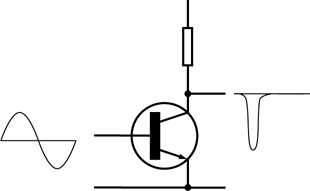
Class B |
|
Class AB |
|
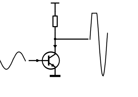
Class C |
|
Class D |
|
Class E |
|
Class F |
|
Class G |
|
Class H |
|
Class S |
|
Totem pole |
|
Distributed amplifier |
|
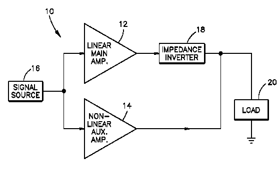
Doherty Amplifier |
|
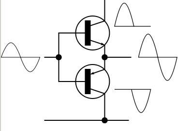
Push Pull |
|
Single Ended Push Pull |
|
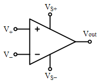
Differential amplifier |
|
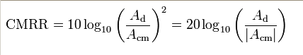
Common mode rejection ratio | the common-mode rejection ratio (CMRR) indicates the ability of the amplifier to accurately cancel voltages that are common to both inputs. The common-mode rejection ratio is defined as: |
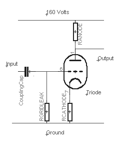
Vacuum tube amplifier |
|
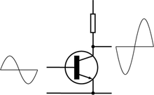
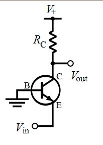
Common emitter/source /cathode |
|
Common base/gate /grid |
|
Cascade coupling |
|
Cascode coupling |
|
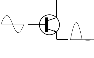
Common collector/drain/anode, i.e. Emitter/source /cathode follower |
|
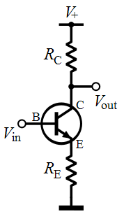
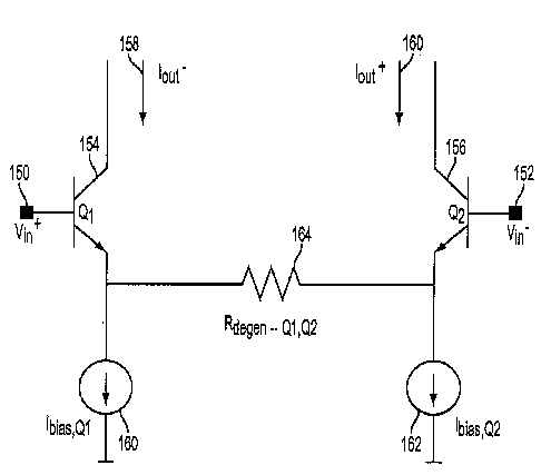
Emitter/Source degeneration |
|
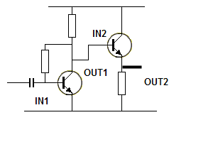
Darlington amplifier |
|
Bridge type |
|
Esaki diode |
|
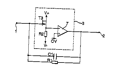
Chopper amplifier |
|
Differential amplifier long tail pair |
|
Differential amplifier PI type |
|
Pseudo differential amplifier |
|
Reflex amplifier |
|
Travelling Wave Tube Amplifier (TWTA) |
|
Klystron |
|
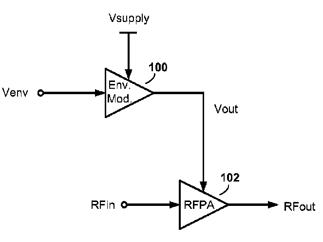
Envelope Elimination and Restoration (EER) |
|
Envelope Tracking (ET) |
|
Charge amplifier |
|


In patent documents, the following abbreviations are often used:
RF | Radio Frequency |
HF | High Frequency, Hoch-Frequenz (German). Haute Fréquence (French) |
NF (German) | Nieder-Frequenz (German) |
NF | Noise Figure |
LF | Low Frequency |
BF (French) | Basse Fréquence (French) |
LNA | Low Noise Amplifier |
MMIC | Microwave Monolithic Integrated Circuit |
IC | Integrated Circuit |
OP-AMP | Operational Amplifier |
FET | Field Effect Transistor |
TEC (French) | Transistor à Effet de Champ (French) |
AC | Alternate Current |
DC | Direct Current |
DAT | Distributed Active Transformer |
SEPP | Single Ended Push Pull |
BALUN | Balanced/Unbalanced or Unbalanced/Balanced |
EMI | Electromagnetic Interference |
ESD | Electro Static Discharge |
TD | Time Domain |
PD | Predistorter |
BiFET | Bipolar and Field Effect Transistor |
CMMR | Common-Mode Rejection Ratio |
CCCS | Current Controlled Current Source |
CCVS | Current Controlled Voltage Source |
VCVS | Voltage Controlled Voltage Source |
VCCS | Voltage Controlled Current Source |
TIA | Trans-Impedance Amplifier |
OTA | Operational Transconductance Amplifier |
TWT | Travelling Wave Tube |
PA | Power Amplifier |
DPA | Doherty Power Amplifier |
MMPA | Multi-Mode Power Amplifier |
TWTA | Travelling Wave Tube Amplifier |
LTP | Long Tailed Pair |
EER | Envelope Elimination and Restoration |
ET | Envelope Tracking |
BTL | Bridged Tied Load |
This place covers:
Details of amplifiers with only discharge tubes, only semiconductor devices or only unspecified devices as amplifying elements, wherein said details are addressing a specific technical effect for the amplification:
Raise the efficiency
Reduce detrimental influences of internal impedances of the amplifying elements
Reduce influence of noise generated by amplifying elements
Reduce influence of variations of temperature or supply voltage or other physical parameters
Reduce non-linear distortion (except when using negative feedback)
Negative feedback with or without positive feedback
Positive feedback without negative feedback
Bandwidth extension
Protection
Modification of input or output impedances
The technical effect is specified according to the IPC definitions for the individual subgroups of H03F 1/00 which follow hereinafter.
A document may be temporarily allocated in the main group H03F 1/00 only for EPO internal circulation, e.g. to receive it from neighbouring field classifiers via the classification code.
This place covers:
Modifications of amplifiers to raise the efficiency, wherein said modification comprises the following techniques:
dynamic bias control based on the input/output signal
supply control based on the input/output signal
selection of one or more amplifiers from a plurality of amplifier
reduction of the number of DC current paths
use of particular circuit topologies, e.g. Doherty amplifier, LINC Amplifier
use of discharge tube amplifiers acting also as modulators.
This place does not cover:
Transmitter circuits with power amplifiers having gain or transmission power control, with means for improving efficiency |
Attention is drawn to the following places, which may be of interest for search:
Amplitude modulation by converting angle modulation to amplitude modulation | |
Gain control details, gain control by varying the supply voltage, gain control dependent on the supply voltage | |
Transmission power control |
This place covers:
Modification of amplifiers to achieve frequency stabilisation or signal isolation among amplifying stages, wherein said modification comprises the following techniques:
use of particular circuit topologies, e.g. transimpendance amplifier, cascode amplifier
use of amplifying elements with multiple electrode connections
use of attenuating means
use of neutralising means, e.g. Miller effect compensation circuitry, pole/zero cancellations in the transfer function
use of distributed coupling
This place does not cover:
Wide-band amplifiers with inter-stage coupling networks incorporating these impedances |
Examples of places where the subject matter of this place is covered when specially adapted, used for a particular purpose, or incorporated in a larger system:
Differential cascode amplifiers, differential folded cascode amplifiers | H03F 3/45089, H03F 3/45094, H03F 3/45103, H03F 3/45107, H03F 3/45116, H03F 3/45121, H03F 3/4513, H03F 3/45134, H03F 3/45143, H03F 3/45147, H03F 3/45156, H03F 3/45161, H03F 3/45188, H03F 3/45192, H03F 3/45201, H03F 3/45206, H03F 3/45215, H03F 3/45219, H03F 3/45228, H03F 3/45233, H03F 3/45242, H03F 3/45246, H03F 3/4526, H03F 3/45255, H03F 3/45286, H03F 3/45291, H03F 3/453, H03F 3/45304, H03F 3/45313, H03F 3/45318, H03F 3/45327, H03F 3/45331, H03F 3/4534, H03F 3/45345, H03F 3/45354, H03F 3/45358, H03F 3/45385, H03F 3/4539, H03F 3/45399, H03F 3/45403, H03F 3/45412, H03F 3/45417, H03F 3/45426, H03F 3/4543, H03F 3/45439, H03F 3/45443, H03F 3/45452, H03F 3/45457 |
Transmitter circuits with power amplifiers having gain or transmission power control, with means for improving efficiency | |
Optical receivers with arrangements for optimising the preamplifier |
Attention is drawn to the following places, which may be of interest for search:
Distributed amplifiers using coupling networks with distributed constants | |
Eliminating transit-time effects in vacuum tubes | |
Gain control in emitter coupled or cascode amplifiers | |
Modifications of control circuit to reduce distortion caused by control | |
Muting circuits | |
Amplitude limiters |
In this place, the following terms or expressions are used with the meaning indicated:
Current steering cascode | cascode amplifier formed by at least two common gate transistors which are both coupled to the drain terminal of the input common source transistor, in order to steer the current at that terminal among different paths. |
In patent documents, the following words/expressions are often used with the meaning indicated:
"cascade" | "cascode". |
This place does not cover:
Modifications of amplifiers to reduce influence of variations of supply voltage in case of switching on or off of a power supply, i.e. popping noise reduction | |
Constructional modification of discharge tubes amplifiers |
Examples of places where the subject matter of this place is covered when specially adapted, used for a particular purpose, or incorporated in a larger system:
Chopper amplifiers | |
Transmitter circuits with means for limiting noise |
This place covers:
Modifications of amplifiers to reduce influence of variations of temperature or supply voltage, or other physical parameters, wherein said modifications comprise:
bias stabilisation circuits
drifting protection circuits
using a switching device and eventually digital means
case of switching on or off a power supply
case of push-pull configuration
This place does not cover:
Differential amplifiers characterised by the way of common mode signal rejection |
Examples of places where the subject matter of this place is covered when specially adapted, used for a particular purpose, or incorporated in a larger system:
Attention is drawn to the following places, which may be of interest for search:
In this place, the following terms or expressions are used with the meaning indicated:
Popping noise | audible noise which is present when switching on or off the power supply |
In patent documents the following expressions are often used as synonyms:
Popping noise | pop effect, plop noise, clic |
This place covers:
Modifications of amplifiers to reduce non-linear distortion, wherein said modifications comprise:
using feedforward circuits
using predistortion circuits, which are implemented with feedback, or via multiple paths, or in audio amplifiers, or with nonlinear elements, or acting on cartesian and polar parameters
case of differential amplifiers
case of single ended push pull amplifiers
This place does not cover:
Modifications of amplifiers to reduce non-linear distortion by negative feedback |
Examples of places where the subject matter of this place is covered when specially adapted, used for a particular purpose, or incorporated in a larger system:
Analog transmitter circuits with power amplifiers with linearisation using predistortion and using feed-forward | |
Analog transmitter circuits with means for limiting distortions | |
Digital transmitters using predistortion |
Indexing Code orthogonal classification
In addition to one or more classification symbols relating to the invention information, where appropriate, one or more Indexing Code symbols relating to orthogonal classification (H03F 2201/3203 - H03F 2201/3236), i.e. covering aspects which are spanning over one or more EC subgroups, should be allocated for the following sub-groups range: H03F 1/32 - H03F 1/3241.
This place covers:
Negative-feedback-circuit arrangements with or without positive feedback, wherein said arrangements comprises:
adaptations for reducing the non-linear distortion
hybrid or directional couplers
transformers.
This place does not cover:
Differential amplifiers for the rejection of common mode signals |
Examples of places where the subject matter of this place is covered when specially adapted, used for a particular purpose, or incorporated in a larger system:
Analog transmitter circuits with means for limiting distortions |
This place covers:
Modifications of amplifiers to extend the bandwidth, wherein the modifications comprise:
periodic amplifiers
aperiodic amplifiers, i.e. wherein aperiodic means that there is no resonant circuit present.
Examples of places where the subject matter of this place is covered when specially adapted, used for a particular purpose, or incorporated in a larger system:
Pulse shaping by amplifying | |
Analog transmitter circuits with means for limiting distortions | |
Optical receivers with bandwidth control |
In this place, the following terms or expressions are used with the meaning indicated:
Inductive peaking | an inductor is placed in the amplifying circuit to extend the bandwidth of amplification. |
This place covers:
Circuit arrangements for protecting such amplifiers, wherein the arrangements comprises:
using redundant amplifying elements
using protective devices, e.g. diodes.
This place does not cover:
Protection from temperature drifting | |
Vacuum tube testing |
Examples of places where the subject matter of this place is covered when specially adapted, used for a particular purpose, or incorporated in a larger system:
Monitoring arrangements | |
Analog transmitter details for increasing reliability |
Attention is drawn to the following places, which may be of interest for search:
Emergency protective circuit arrangements | |
Over voltage protection in integrated circuits | |
Frequency-division multiplex system with monitoring arrangements |
This place covers:
Modifications of input or output impedances, not otherwise provided for, wherein said modifications may comprise:
matching and tuning circuits which are specifically designed for RF amplifiers
circuit adaptations in class E,F,E/F amplifiers.
Examples of places where the subject matter of this place is covered when specially adapted, used for a particular purpose, or incorporated in a larger system:
High frequency amplifiers | |
Switching amplifiers in general | |
Class E amplifiers | |
Amplifiers in which coupling networks have distributed constants |
Attention is drawn to the following places, which may be of interest for search:
Matching with passive networks | |
Matching with active networks |
This place covers:
Electronic amplifiers based on tubes or semiconductors.
Amplifiers are classified according to topology (e.g., push-pull, emitter follower, differential) and/or according to use (e.g., LF, HF) and/or according to the amplifying element (e.g., tubes, tunnel diodes) and/or according to special functionality (e.g., multi-channel amplifiers, gated amplifiers).
Amplifiers with both tubes and semiconductors are classified in H03F 5/00.
Amplifiers based on other amplification principles such as magnetic, dielectric, mechanical/acoustic, superconductivity, etc., are classified in subgroups H03F 7/00-H03F 99/00.
A document may be temporarily allocated in the main group H03F 3/00 only for EPO internal circulation, e.g. to receive it from neighbouring field classifiers via the classification code.
This place covers:
Amplifiers with switched capacitors used as synthesized resistors.
This place does not cover:
Attention is drawn to the following places, which may be of interest for search:
Switched capacitor filters |
This place covers:
Amplifiers controlled by light, that is, for optically generated or transferred signals, e.g., transimpedance amplifiers for fiber optic links, optical isolation amplifiers.
Examples of places where the subject matter of this place is covered when specially adapted, used for a particular purpose, or incorporated in a larger system:
Optical receivers |
This place covers:
Amplifiers controlled by light, wherein the amplifier comprises FETs, e.g., JFET or CMOS transimpedance amplifiers for fiber optic links.
This place covers:
Amplifiers controlled by light, wherein the amplifier comprises optically coupled stages, e.g., optical isolating amplifiers.
This place covers:
Amplifiers controlled by light, wherein the amplifier has functional units such as op-amps, i.e., not showing transistor level circuit details.
This place covers:
Amplifiers using diodes as an amplifying element, e.g., negative resistance diodes such as Gunn, IMPATT, Esaki (tunnel) diodes.
This place does not cover:
Switching amplifiers with freewheeling diodes |
This place covers:
Amplifiers using Esaki (tunnel) diodes as an amplifying element.
This place covers:
Amplifiers with semiconductor amplifying devices having more than three electrodes, e.g., dual-gate MOSFETs, back-gate controlled MOSFETs, multi-emitter/collector BJTs. Note: by semiconductor amplifying devices is understood transistors; opamps and the like are not included, even if they have more than three terminals. Cascode amplifiers using dual-gate MOSFETs are classified in H03F 1/223.
This place covers:
Amplifiers with semiconductor field-effect amplifying devices, e.g., MOSFETs, JFETs, MESFETs.
This place covers:
Amplifiers with semiconductor junction field-effect amplifying devices, e.g., JFETs, MESFETs (but not MOSFETs).
This place covers:
Low frequency amplifiers, in most cases which are suitable for amplification of audio signals.
Attention is drawn to the following places, which may be of interest for search:
Switching amplifiers | |
Gain control in low frequency amplifiers | |
Circuits for loudspeakers, microphones |
This place covers:
High frequency amplifiers, e.g. radio frequency amplifiers, as detailed circuits or integrated circuit blocks.
Examples of places where the subject matter of this place is covered when specially adapted, used for a particular purpose, or incorporated in a larger system:
Amplifiers in which coupling networks have distributed constant | |
IF amplifier circuits specially adapted for B&W TV |
Attention is drawn to the following places, which may be of interest for search:
Switching amplifiers | |
Gain control in high frequency amplifiers, bandpass amplifiers | |
High frequency adaptations of semiconductors |
In patent documents, the following abbreviations are often used:
HBT | Heterojunction Bipolar Transistor |
HEMT | High Electron Mobility Transistor |
This place covers:
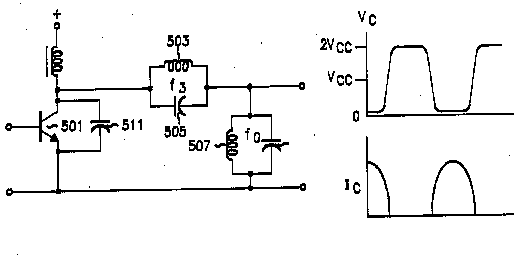
Power amplifiers in general. e.g. class B amplifiers, Class C amplifiers, Class D amplifiers, Class E amplifiers, Class F amplifiers, Class G amplifiers, Class H amplifiers, Class S amplifiers, or combination of power amplifiers, or integrated circuits wherein the circuit topology is based on lumped elements.
This place does not cover:
Push pull amplifiers | |
Single ended push pull amplifiers | |
Combination of amplifiers in which coupling networks have distributed constant |
Examples of places where the subject matter of this place is covered when specially adapted, used for a particular purpose, or incorporated in a larger system:
Multi-channel amplifiers | |
Analog transmitters | |
Digital transmitters |
Documents which are addressing a power amplifier in general are usually not classified in this subgroup, but are allocated to the corresponding subgroups:
Indexing Code deep-indexing classification
In addition to one or more classification symbols relating to the invention information, where appropriate, one or more Indexing Code symbols relating to deep-indexing classification (H03F 2203/21103 - H03F 2203/21196), i.e. covering embodiment aspects, should be allocated for the following sub-group: H03F 3/211
This place covers:
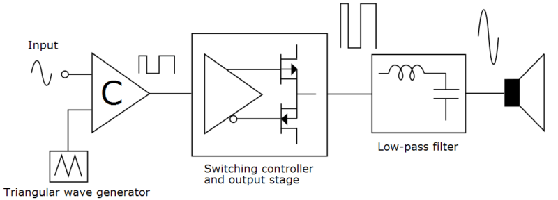
Amplifiers using switches as amplifying elements, e.g., class D audio amplifiers, class E, class F, class S RF amplifiers, as well as control circuitry such as PCM-PWM conversion etc.
This place does not cover:
Examples of places where the subject matter of this place is covered when specially adapted, used for a particular purpose, or incorporated in a larger system:
MRI gradient amplifiers | |
DC-AC converters | |
Deaf-aid sets | |
Stereophonic systems |
Multiple classification symbols may be given, e.g., a stereo full-bridge class D audio power amplifier with protection means and anti pop-noise means would be classified in H03F 3/68, H03F 3/2173, H03F 1/52, H03F 1/305, and possibly also somewhere in H04S. A class D MRI gradient amplifier would be classified in both G01R 33/3852 and H03F 3/217. An RF amplifier with a class D amplifier used as a tracking power supply (aka class S) would be classified in the relevant H03F 1/02 sub-group, as well as in H03F 3/217 (provided that the class D amplifier is shown in some detail), and possibly also in H03F 3/189, for example.
This place covers:
Switching amplifiers using FET switches as amplifying elements.
This place covers:
Switching amplifiers with half- or full-bridges.
This place covers:
Switching amplifiers for digital input signals, or having explicit ADCs or DACs.
This place covers:
Class E RF amplifiers.
This place does not cover:
Class F RF amplifiers (see the "Glossary of terms" section above). These are classified in other relevant H03F 3/217 subgroups.
This place covers:
Switching amplifiers with one or more switches (e.g., segmented transistors in RF amplifiers) or output stages (such as in staggered phase class D amplifiers) in parallel or in series, cooperating to produce a common output signal.
This place does not cover:
Combinations of a switching amplifier and a linear amplifier to produce a single output signal (but a H03F 3/217 sub-group should still be given, by virtue of the switching amplifier). | |
Multi-channel amplifiers |
This place covers:
Power amplifiers with tubes (thermionic valves only).
This place does not cover:
Tube power amplifiers for radio transmitters | |
Tube push-pull amplifiers (two tubes connected to either side of a transformer primary with a center tap connected to a supply voltage and driven out of phase). | |
Tube single-ended push-pull amplifiers (tubes connected in series across two supply rails and the output signal taken at the node common to the tubes) |
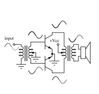
This place covers:
Push-pull amplifiers (see the push-pull configuration in the "Glossary of terms" section above) and phase-splitters therefor, i.e. the phase splitter circuitry which is suitable for driving them.
This place does not cover:
Duplicated single-ended push-pull arrangements or phase-splitters therefor | |
Single-ended sense amplifiers |
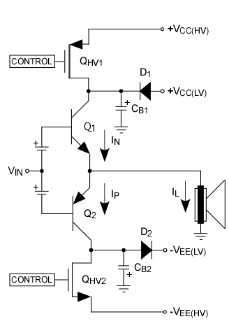
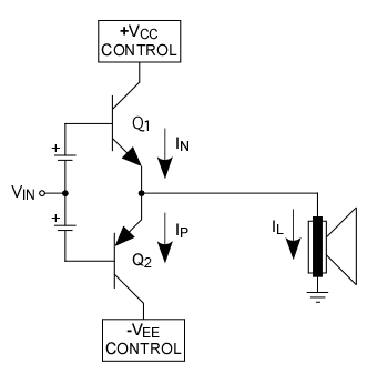
This place covers:
Single-ended push-pull amplifiers (see the SEPP configuration in the "Glossary of terms" section above) and phase-splitters therefor, i.e. the phase splitter circuitry which is suitable for driving them.
This place does not cover:
Switching amplifiers | |
Single-ended sense amplifiers |
It must be noted that the expression "common drain output", which is present in the definition of subgroup H03F 3/301, relates to a common drain configuration for the output transistors (see the "Glossary of terms" section above), therefore it relates to the source terminals of the output transistors being tied together to form the output terminal.
Similar consideration applies for the expression "common source output", which is present in the definition of subgroup H03F 3/3022, and which relates to a common source configuration of the output transistors (see the "Glossary of terms" section above), i.e. the drain terminals of the output transistors being tied together to form the output terminal.
Furthermore, in the following subgroups the expression "symmetrical driving of the end stage" is present:
From a circuital topology point of view, it relates to the presence of symmetry in the driving stage circuitry of the SEPP, i.e. if the driving signal path for one of the output transistor has the same/corresponding/complementary elements of the driving signal path of the other output transistor.
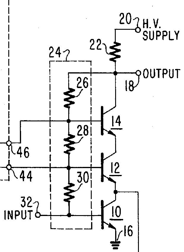
As clarifying example the following circuit topology is shown.
Example of SEPP with symmetrical driving of the end stage (drawing extracted from US2002109548).
Mostly of the times the presence of symmetry can be easily detected on the circuit topology by considering a virtual axis (see the dotted line "Symmetry axis" in the drawing above) passing through the output terminal to determine two sub-circuits which are located above and below said axis, respectively, and by examining the similarities/corresponding elements among the two sub-circuits.
If no symmetry is detected then the SEPP circuit is of the type having "asymmetrical driving of the end stage" and it has to be classified in one of the following subgroups:
Furthermore, it must be noted that, when two SEPPs are configured as class B or AB bridges, they are classified in H03F 3/3081 and when they are implemented with FETs they are classified in H03F 3/3061. Switching amplifiers in bridge configuration are classified in H03F 3/2173.
Indexing Code orthogonal classification
In addition to one or more EC symbols relating to the invention information, where appropriate, one or more Indexing Code symbols relating to orthogonal classification (H03F 2203/30003 - H03F 2203/30156), i.e. covering aspects which are spanning over one or more EC subgroups, should be allocated for this subgroup.
This place covers:
DC amplifiers which are formed by IC blocks, semiconductors or tubes, in which all the amplifying stages are DC coupled, e.g. without using capacitive or switching elements, which are not specific for RF amplifiers or audio amplifiers and which have circuit topologies that are not related to other H03F classification symbols.
This place does not cover:
Differential amplifiers |
Examples of places in relation to which this place is residual:
Low frequency amplifiers | |
High frequency amplifiers | |
Power amplifiers |
Attention is drawn to the following places, which may be of interest for search:
DC current or voltage control circuits |
This place covers:
DC amplifiers wherein only the AC signal is passed through the amplifying units, the DC signal is decoupled via switching elements, e.g. see the Chopper amplifier configuration in the "Glossary of terms" section above.
This place does not cover:
Switched capacitor amplifiers |
Examples of places where the subject matter of this place is covered when specially adapted, used for a particular purpose, or incorporated in a larger system:
Switching amplifiers | |
Differential amplifiers | |
Arrangements for measuring bio-electric currents or voltages | |
Arrangements for measuring currents or voltages or for indicating presence or sign thereof by using conversion of DC into AC |
Attention is drawn to the following places, which may be of interest for search:
This place covers:
In most cases totem-pole amplifiers, see the "Glossary of terms" section above, which are implemented via semiconductor elements or tubes.
This place covers:
Differential amplifiers in general and characterised by the technology used, the circuit topologies, and the way that the common mode signals are rejected.
This place does not cover:
Measuring currents or voltages from sources with high internal resistance by means of measuring circuits with high input impedance, e.g. OP-amplifiers | |
Operational amplifiers for addition or subtraction in analog calculators | |
Differential sense amplifiers | |
Logic comparators | |
Optical receivers with offset control of the differential preamplifier | |
Differential drivers |
Attention is drawn to the following places, which may be of interest for search:
Gain control in emitter coupled or cascode amplifiers | |
Tuned filters, switched capacitor networks |
Pseudo differential amplifiers (see the "Glossary of terms" section above) are usually classified in H03F 3/4508, H03F 3/45179, H03F 3/45278, H03F 3/45376.
Furthermore, it is common practice at EPO, when classifying semiconductor differential amplifiers, to consider first the technology of the amplifying transistors and the circuit topology information, in order to classify under one of the subgroups belonging to H03F 3/45076.
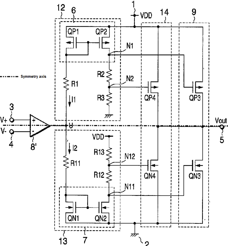
About circuit topology, the expression "Complementary long tailed pairs having parallel inputs and being supplied in parallel" is present in the following subgroups:
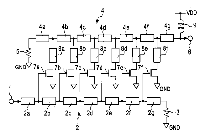
As clarifying example the following circuit topology is shown:
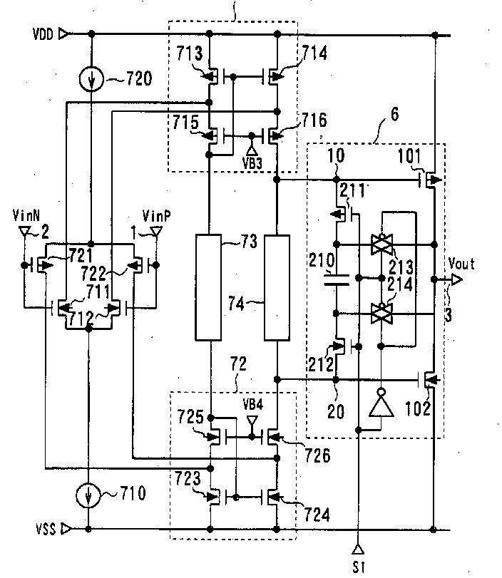
Example of differential amplifier with complementary long tailed pairs having parallel inputs and being supplied in parallel: the first transistor pair (711,712) and the second transistor pair (721,722) constitute two complementary transistor pairs, which, together with the corresponding current sources (710,720) constitute long tail pairs (see the "Glossary of terms" section above), and wherein said pairs have parallel inputs (see the common input terminals (VinN, VinP) and are supplied in parallel (see the common supplies VDD, VSS), (drawing extracted from US2005040889).
Similar consideration applies to the expression "Complementary PI types having parallel inputs and being supplied in parallel", wherein the complementary transistor pairs are forming differential amplifiers of the PI type, (see the "Glossary of terms" section above), and which are classified in the following subgroups:
About the expression "Complementary long tailed pairs having parallel inputs and being supplied in series", which is present in the following subgroups:
As clarifying example the following circuit topology is shown:
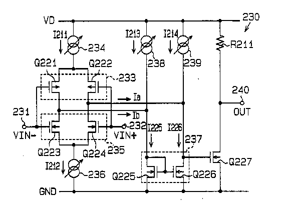
Example of differential amplifier with complementary long tailed pairs having parallel inputs and being supplied in series: the first transistor pair (Q221,Q222) and the second transistor pair (Q223, Q224) constitute two complementary transistor pairs, which, together with the corresponding current sources (234,236) constitute long tail pairs (see the "Glossary of terms" section above), and wherein said pairs have parallel inputs (see the common input terminals (VIN-, VIN+) and are supplied in series (see the series connecting path from VD to GND, which is formed by element 234, the first transistor pair (Q221,Q222), the second transistor pair (Q223, Q224), element 236), (drawing extracted from FR2814554).
Similar consideration applies to the expression "Complementary PI types having parallel inputs and being supplied in series", wherein the complementary transistor pairs are forming differential amplifiers of the PI type, (see the "Glossary of terms" section above), and which are classified in the following subgroups:
Once that the technology and the circuit topology related to the differential amplifier are classified, a possible classification under one of the subgroups belonging to H03F 3/45479 has to be considered. It must be noted that the expression "common mode signal rejection", which is present in the definition of subgroup H03F 3/45479, has to be interpreted with a broader meaning than the one used in common practice (see the "Glossary of terms" section above). In practice common mode rejection has to be meant as operating point/DC level control/offset reduction, and said control can be implemented at sub-circuit level.
Hence all the subgroups of H03F 3/45479 are addressing all the possible implementations of said common mode rejection within the sub-circuits that are forming the differential amplifier architecture (for a detailed definition of said sub-circuits see the following section).
Indexing Code orthogonal classification
In addition to one or more EC symbols relating to the invention information, where appropriate, one or more Indexing Code symbols relating to orthogonal classification (H03F 2203/45002 - H03F 2203/45732), i.e. covering aspects which are spanning over one or more EC subgroups, should be allocated for this subgroup.
Said aspects are mainly based on the following sub-circuits, which can be determined in a long tailed pair, PI type, and, although with limitations, in special types of differential amplifiers, e.g. pseudo-differential amplifier:
AAC = Active Amplifying Circuit, i.e. the elements comprising the amplifying transistors.
CSC = Common Source Circuit, i.e. the elements forming the long tailed circuit or the PI circuit.
IC = Input Circuit, i.e. the elements coupled to the input terminals of the amplifying transistors.
LC = Loading Circuit, i.e. the elements coupled to the output terminals of the amplifying transistors.
CMCL = Common Mode Controlling Loop, i.e. the elements which are controlling the common mode(s) of the differential amplifier.
FBC = Feed-Back Circuit, i.e. the elements which are introducing feedback signal(s) for the differential amplifier.
Here is an example of some of said sub-circuits above for a long tailed differential pair.
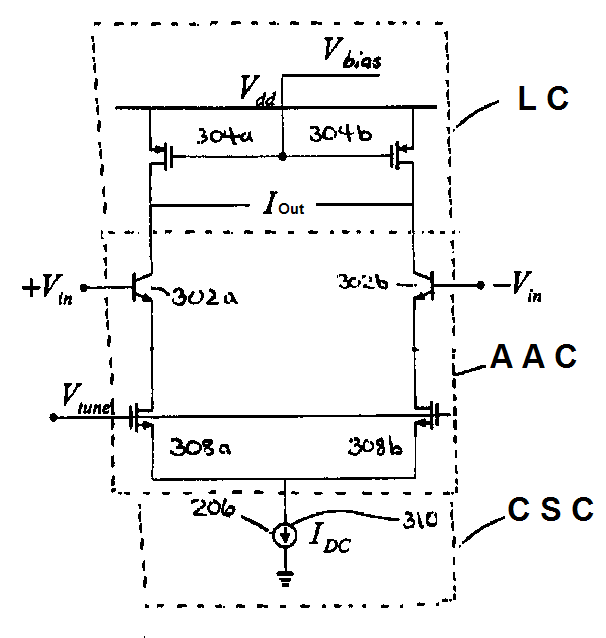
drawing derived from US2006055463
This place covers:
Reflex amplifiers, see the "Glossary of terms" section above, which are implemented via semiconductor elements or tubes.
This place does not cover:
Reflection amplifiers |
Examples of places where the subject matter of this place is covered when specially adapted, used for a particular purpose, or incorporated in a larger system:
Receivers comprising at least one semiconductor device having three or more electrodes |
This place covers:
Amplifiers in cathode follower, source follower, emitter follower configuration (see the "Glossary of terms" section above).
Examples of places where the subject matter of this place is covered when specially adapted, used for a particular purpose, or incorporated in a larger system:
Delay circuits |
Indexing Code deep-indexing classification
In addition to one or more classification symbols relating to the invention information, where appropriate, one or more Indexing Code symbols relating to deep-indexing classification (H03F 2203/5003 - H03F 2203/5045), i.e. covering embodiment aspects, should be allocated for this subgroup.
This place covers:
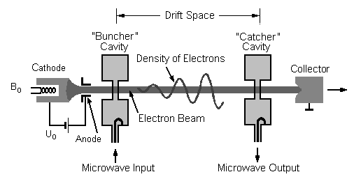
Amplifiers using transit-time effects, mostly Klystrons or Travelling Wave Tubes (TWT) see the "Glossary of terms" section above.
Examples of places where the subject matter of this place is covered when specially adapted, used for a particular purpose, or incorporated in a larger system:
Solid state travelling-wave devices |
Attention is drawn to the following places, which may be of interest for search:
Parametric amplifiers | |
Travelling wave tubes in general | |
Resonators of the waveguide type |
This place covers:
Amplifiers having distributed coupling networks, e.g. transmission lines, the so called microwave amplifiers.
This place does not cover:
Examples of places where the subject matter of this place is covered when specially adapted, used for a particular purpose, or incorporated in a larger system:
Class E amplifiers | |
Reflex amplifiers | |
Multi-channel amplifiers | |
Aerials or aerial systems providing at least two radiating patterns, beam-forming means |
Attention is drawn to the following places, which may be of interest for search:
Modification of amplifiers by use of distributed coupling, i.e. distributed lumped elements | |
Amplifiers having more than three electrodes with field-effect devices | |
High frequency amplifiers | |
Coupling devices of the waveguide type | |
High frequency adaptations of semiconductors |
This place covers:
Two-way amplifiers, which are implemented via semiconductor elements or tubes and which are typically employed to amplify the signal levels of forward and reverse signals.
This place covers:
Amplifying-mixing devices for achieving a special technical effect, e.g. interference reduction.
This place covers:
Stereo amplifiers or multi-channel amplifiers in the low frequency range.
Multi-band amplifiers in the high frequency range, wherein multiple outputs are present.
This place does not cover:
Aerials, beam-forming means | |
Circuits for stereophonic arrangements |
Attention is drawn to the following places, which may be of interest for search:
Low frequency amplifiers | |
Power amplifiers using a combination of several semiconductor amplifiers | |
Switching amplifiers | |
Combinations of amplifiers using coupling networks with distributed constants |
This place covers:
Charge amplifiers, see the "Glossary of terms" section above.
This place does not cover:
Charge pumps for DC/DC power converters | |
Charge pumps for automatic control of frequency or phase circuits |
Examples of places where the subject matter of this place is covered when specially adapted, used for a particular purpose, or incorporated in a larger system:
Measuring acceleration by piezoelectric pick-up | |
Integrators using operational amplifier and capacitor and resistor in the feedback loop | |
Sense amplifiers |
This place covers:
Amplifiers which are enabled or disabled by means of a control signal, e.g. via a controlled switch.
Attention is drawn to the following places, which may be of interest for search:
Gain control in amplifiers | |
Electronic switching or gating |
Indexing Code deep-indexing classification
In addition to one or more classification symbols relating to the invention information, where appropriate, one or more Indexing Code symbols relating to deep-indexing classification (H03F 2203/7203 - H03F 2203/7239), i.e. covering embodiment aspects, should be allocated for this subgroup.
This place covers:
Parametric amplifiers, i.e. wherein a component parameter such as capacitance or inductance is varied to achieve amplification.
Attention is drawn to the following places, which may be of interest for search:
Amplifiers using superconductivity effects | |
Devices or arrangements for the parametric generation or amplification of light, infrared or ultraviolet waves |
This place covers:
Parametric amplifiers where inductance/permeability is varied to achieve amplification.
This place covers:
Parametric amplifiers where capacitance/permittivity is varied to achieve amplification.
This place covers:
Amplifiers using saturable reactors as amplifying elements (aka mag-amps).
This place covers:
Magnetic amplifiers where an AC load current flows in a main coil, controlled by the current in a control coil.
This place covers:
Magnetic amplifiers where a load current flows in one direction in a main coil, and typically in the other direction in another main coil, controlled by the current in a control coil, e.g., a control coil in a center leg of a transformer controlling two main coils in two outer legs.
This place covers:
Magnetic amplifiers where the load current is auto-commutated by the main coil, the core being periodically reset by a control coil.
This place covers:
Amplifiers using non-linear (hysteretic) dielectric elements to achieve amplification.
This place covers:
Amplifiers with intermediate mechanical or acoustic energy transfer .
This place covers:
Amplifiers relying on galvano-magnetic effects, i.e., which arise when a conductor or semiconductor placed in a magnetic field carries current, such as the Hall-effect.
This place covers:
Amplifiers relying on intermediate transformation into light to achieve amplification.
This place does not cover:
Amplifiers controlled by light, e.g., for fiber optic links | |
Amplifiers with optical coupling between stages |
This place covers:
Amplifiers not covered elsewhere, e.g. relying on radioactivity or using esoteric semiconductor structures.