CPC Definition - Subclass H01P
This place covers:
Passive devices which have electrical dimensions comparable with the working wavelength, and which operate at frequencies up to but not including optical frequencies, e.g. microwave, and their manufacture.
Auxiliary devices of waveguide type such as filters, phase shifters, non-reciprocal devices, polarisation rotators.
Tubular waveguides and transmission lines such as strip lines, microstrips, coaxial lines, dielectric waveguides.
Devices for coupling between waveguides, transmission lines or waveguide type devices.
Resonators of the waveguide type.
Delay lines of the waveguide type.
Apparatus or processes specially adapted for manufacturing waveguides, transmission lines, or waveguide type devices.
Waveguides and waveguide type devices are commonly associated with antennas and aerials, these are classified in H01Q.
This place does not cover:
Devices operating at optical frequencies |
Attention is drawn to the following places, which may be of interest for search:
Coaxial cables | |
Transit-time tubes | |
Aerials | |
Quasi-optical devices | |
Line connectors | |
Cable fittings | |
Networks comprising lumped impedance elements |
In this place, the following terms or expressions are used with the meaning indicated:
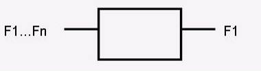
Auxiliary devices | Devices which perform an operation other than the mere simple transmission of energy. |
Waveguide type | As applied to transmission lines, this term includes only high-frequency coaxial cables or Lecher lines, and as applied to resonators, delay lines, or other devices, this term includes all devices having distributed inductance and capacitance. |
In patent documents, the following abbreviations are often used:
Non-reciprocal devices | Components such as circulators or isolators, using the propagation properties of ferrites. |
This place covers:
Any kind of transmission line provided with diodes, where the use of the diodes will change the transmission line behaviour.
Attention is drawn to the following places, which may be of interest for search:
Transference of modulation using distributed inductance capacitance | |
By means of diodes | |
Mounted on a stripline circuit | |
Located in a hollow waveguide |
This place covers:
Non movable joints, direct (non-electromagnetic) couplings between transmissions lines and/or circuits:
Attention is drawn to the following places, which may be of interest for search:
Coaxed connectors specifically adapted for high frequency |
Illustrative example of subject matter classified in H01P 1/045:
This place covers:
Coplanar waveguide/slot joints; multi-level connections (also via short coaxial section).
This place covers:
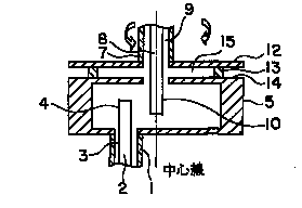
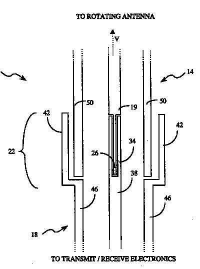
Movable connections between transmission lines and/or other microwave elements; chokes, seals, electromagnetical coupling.
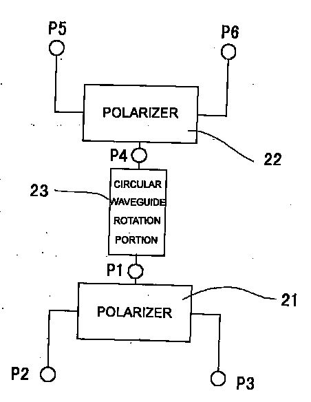
Using mechanical rotation for polarisation rotation: H01P 1/165.
This place covers:
Aperture in a waveguide to insulate microwave circuits from differential pressures, but they enable the propagation of microwaves without introducing reflection or internal resonance.
Windows of the kind which serve to isolate the environment without a section of electromagnetic transmission line from another environment of different pressures and/or other environmental conditions, and which allow electromagnetic energy travelling along the transmission line to pass through the window with little or no loss of power.
- H01H (related to switches);
- H01H 59/00 (MEM's).
In this place, the following terms or expressions are used with the meaning indicated:
MEM | Microelectromechanical (switches) |
BAW | Bulk Acoustic Wave |
This place covers:
Anisotropic media: Media where the vectors E and D are nonparallel and/or nonparallel H and B vectors, which means that the media has different electrical properties in different directions, and thus the permittivity and/or permeability has a matrix form.
Ferrites are ferromagnetic ceramic materials, compounds of iron, boron and barium or strontium or molybdenum. Ferrites have a high magnetic permeability, which allows them to store stronger magnetic fields than iron, and are known as ceramic magnets.
Applying a DC magnetic bias field to a ferrite will produce that a microwave signal will propagate differently in different directions, this effect can be utilized to fabricate directional devices as isolators, circulators and gyrators. The interaction with an applied microwave signal can be controlled by adjusting the strength of the bias field, which leads to a variety of control devices such as phase shifters, switches and tunable resonators and filters.
This place covers:
Mechanical switches (can be electrically or magnetically controlled); redundancy switches; distribution of signals; channel selection; also mechanical aspects of switchable attenuators, filters, etc.; choking aspects.
MEMS in H01H 1/0036, H01H 59/0009.
MEMS in H03H 9/2405 and H03H 3/0072.
This place covers:
Triggering plasma; multipactor switch; generating electron beams; use as receiver protector.
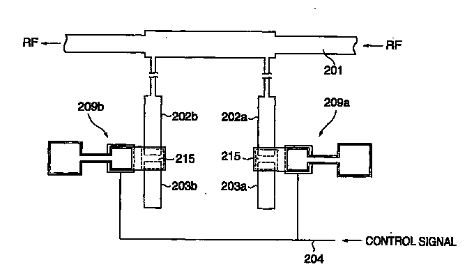
This place covers:
(varactor) diodes; optically controlled semiconductors; use as transmit/receive switch.
This place does not cover:
Optically controlled | |
Electronic switching or gating...in bipolar transistor switches; | |
Electronic switching or gating....switching arrangements with several input- or output-terminals. | |
Switches using semiconductor devices | |
Using Fets, Field effect transistors | |
Using Diodes |
This place covers:
Orthomode transducer: a three port waveguide device which supports signals having two orthogonal modes.
This place does not cover:
Orthomode horns |
This place does not cover:
Rotation in free space |
This place covers:
linear <--> circular polarisation; (gradual) change of waveguide inner surface; meandering conductors in a waveguide.
See also H01Q 15/244.
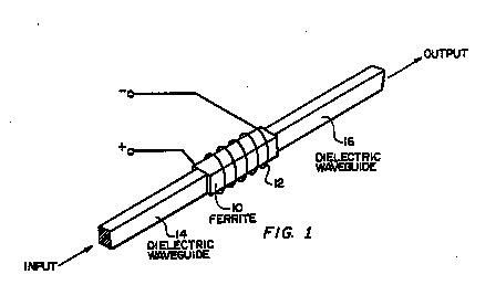
This place covers:
Faraday rotation is the rotation of the plane of polarization of microwave energy exhibited when the energy is transmitted through ferrite material in the direction of a magnetic field.
A ferrite rod is included within the waveguide and is usually surrounded by an electrical coil to provide a magnetic field. By adjusting the plane of polarisation of the microwave radiation, its propagation along the waveguide may be controlled.
This place does not cover:
For rotating the plane of polarization |
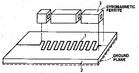
This place covers:
Microstrip, slotlines, coplanar lines phase shifters are included in this group.
Attention is drawn to the following places, which may be of interest for search:
Modulating electromagnetic waves using semiconductor devices |
This place covers:
Non-reciprocal devices; ferrites.
This place covers:
This classification is very general, only related to filters that can not be clearly included in any of the following classifications or to theoretic articles/application where no specific filter arrangement (microstrip, stripline, waveguide, coaxial, coplanar, etc...) has been specified.
Bandpass or band-pass filters.
Low-pass or lowpass filters.
High-pass or highpass filters
Attention is drawn to the following places, which may be of interest for search:
Metamaterials | |
Laser and terahertz frequencies | |
Low frequency filters | |
Filtering due to the substrate |
In patent documents, the following words/expressions are often used as synonyms:
- "Bandpass" and "band-pass"
- "Low-pass" and "lowpass"
- "Band-stop or bandstop", "band reject","notch filter" and "band elimination"
- "High-pass" and "highpass filter"
This place covers:
Filters implemented in a dielectric waveguide, e.g. NRD nonradiative dielectric waveguide.
The NRD guide circuit (Non-radiative dielectric waveguide) has a structure with a dielectric line through which an electromagnetic wave is transmitted and it is sandwiched between two parallel conductive plates made from conductive metal. A space of the two parallel plates is less than half a free space wavelength of a using frequency. Accordingly, the electromagnetic wave is blocked in plates other than the dielectric line and its radiation is restricted, so that the NPD guide circuit can transmit the electromagnetic wave along the dielectic line at a small loss.
In patent documents, the following abbreviations are often used:
NRD | Non-Radiative Dielectric |
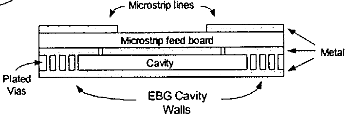
This place covers:
A structure that possesses a dispersion relation having a bandgap in which propagation of electromagnetic waves is prohibited in a specified frequency band is called an electromagnetic bandgap structure.
A photonic bandgap structure is a periodic arrangement of "defects" (e.g., pits or holes formed in layer of a device) that prevents the propagation of all electromagnetic waves within a particular frequency band. The defects introduce electrical frequency stop-bands much like a Bragg grating or crystal lattice structure introduces stop-bands in an optical transmission system. The spacing of the photonic bandgap structure's periodic defects determines the stop-band frequencies.
An electromagnetic bandgap* structure (EBG) is recently receiving attention as a scheme to solve some noise problems in microwave applications. This is for the purpose of blocking a signal ranging a certain frequency band by arranging the EBG having a certain structure in a printed circuit board, and the typical EBG has roughly two, namely a Mushroom type EBG(MT-EBG) and a Planar type EBG(PT-EBG).
* To have a better explanation of the electromagnetic bandgaps, see XP11037787, XP1034579
This EBG structure functions as a magnetic wall that reflects incident electromagnetic waves in phase in the vicinity of the band gap frequency band. For this reason, by installing the EBG structure on the back surface of an antenna, it is possible to achieve a lower profile of the antenna while maintaining its radiation efficiency.
(Internal Note: reference is made to KW: 1500C5E included in H01Q)
H05K 1/0236: Frequency selective surfaces to shield the noise coming from inside the PCB.
When meta materials are included in the PCB see H05K 1/024.
The metamaterial is an artificial substance having an electromagnetic or optical characteristic which is not provided in substances existing in the natural world. Representative characteristics of such a metamaterial include negative magnetic permeability ([mu]<0), negative dielectric constant ([element of]<0), or negative refractive index (in a case where both of the magnetic permeability and the dielectric constant are negative).
In this place, the following terms or expressions are used with the meaning indicated:
EBG | Electromagnetic Bandgap |
PBG | Photonic Bandgaps |
This place covers:
The filtering devices including lumped elements, or striplines or coaxial implementations.
This place covers:
One input and one output frequency (filtered).
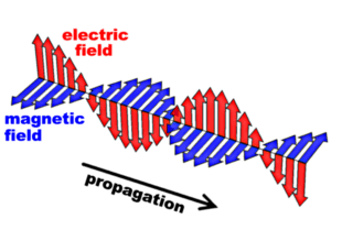
The basic transverse electromagnetic wave involves both a varying electric field and a varying magnetic field, appearing at right angles to each other and to the direction of travel of the wave.
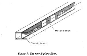
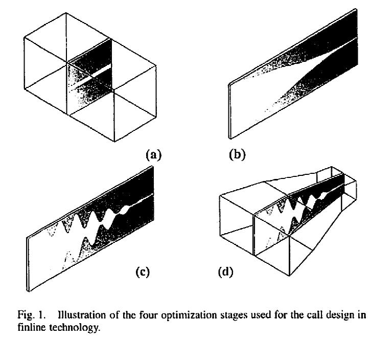
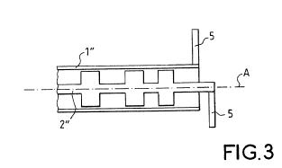
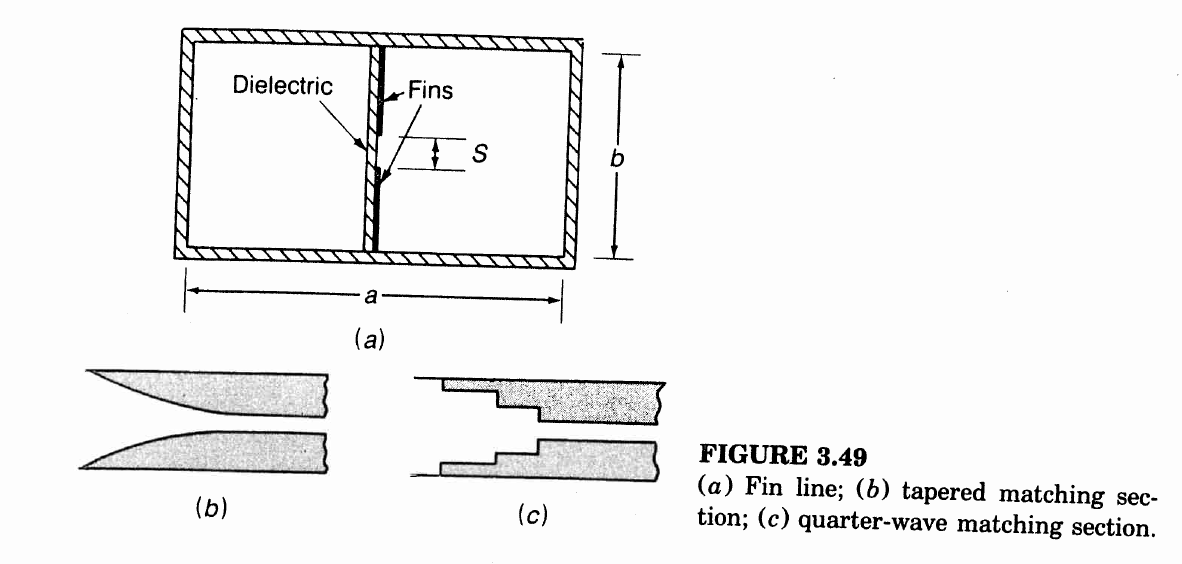
This place covers:
Fin-line and metal insert filters, see XP 1401427.
In a fin-line structure metal inserts (fins) are printed on a dielectric substrate mounted in the E-plane of a rectangular waveguide.
This place does not cover:
In the case of an E-plane waveguide filter, if the element dividing the waveguide is a "metal plate" | |
Sometimes, E-plane filters with a metal plate dividing the two halves of the waveguide is considered also as "finline filter". In this case (if there is a "metal plate"), classify it in |
This place does not cover:
SAW (Surface Acoustic Wave) filters |
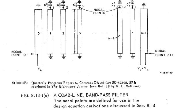
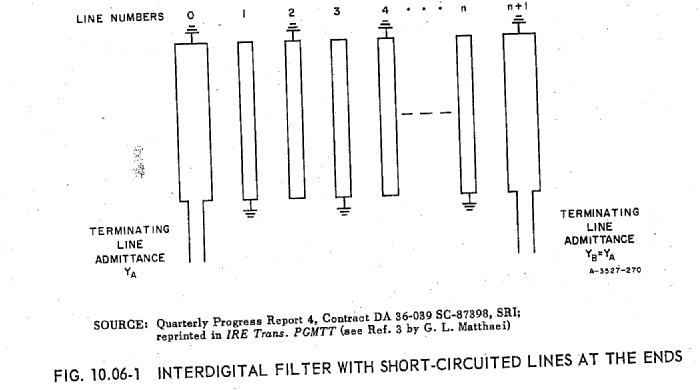
This place covers:
The definition of this class relates to the configuration of the filters and the arrangement of the connection to ground (see figures).
This place covers:
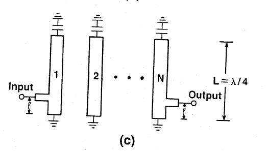
The filters are arranged in a plurality of stacked layers, where "usually" the ground planes are the external (bottom/top layers) ones.
This place covers:
The input and the output of the filter are arranged in a linear configuration.
This place covers:
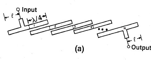
All kind of stripline filters (trapezoidal, helicoidal, spiral, etc...) not included in any of the previous classifications.
This place covers:
Low pass filter.
notch, bandstop filter
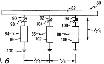
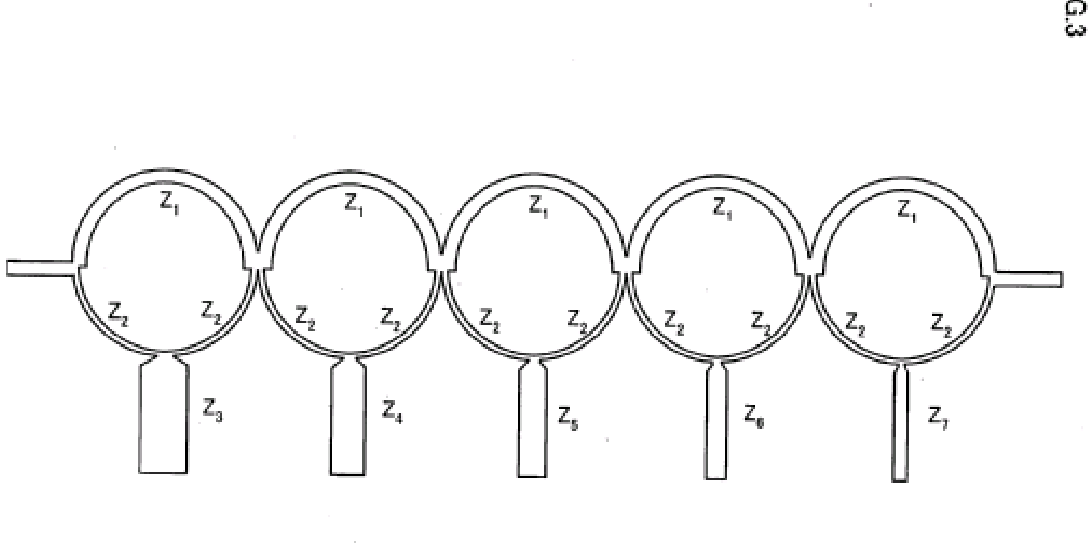
Bandpass filters using ring resonators with different notch frequencies connected in parallel (see US2007/0063794).
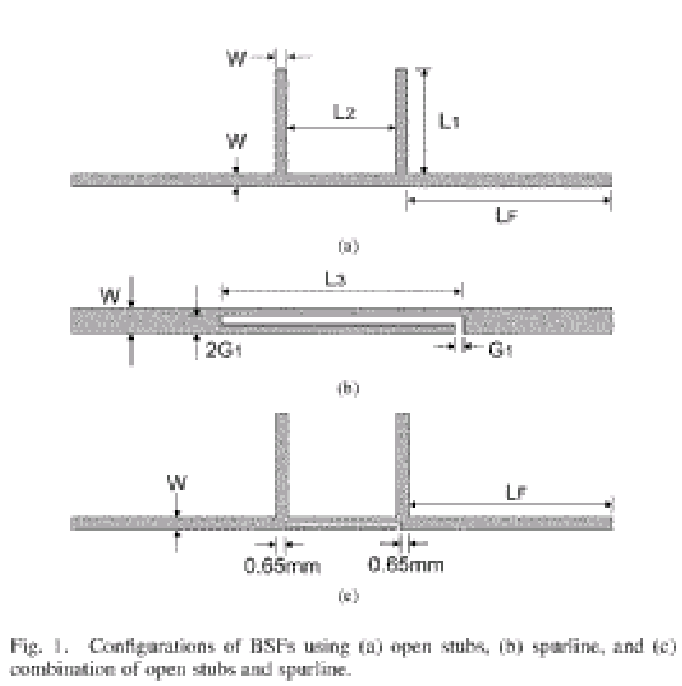
Bandstrop filters with spurlines (spur lines).
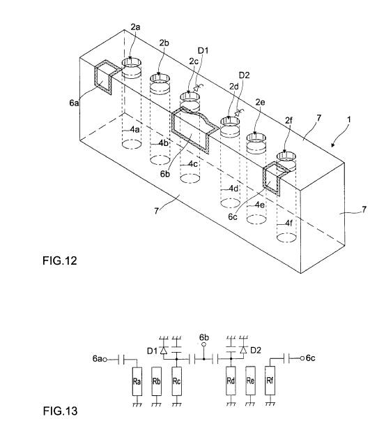
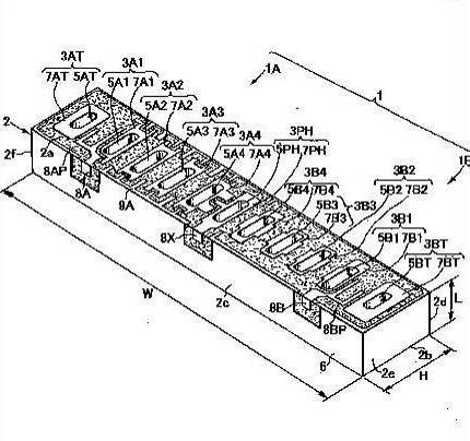
This place covers:
In this configurations, each resonator has its own external conductive wall.
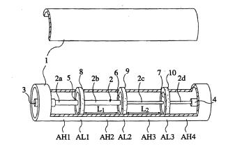
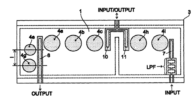
Cascaded dielectric coaxial resonators
Cascaded cavities with coaxial resonators
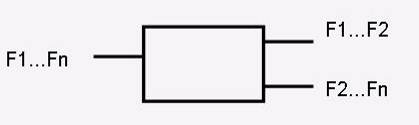
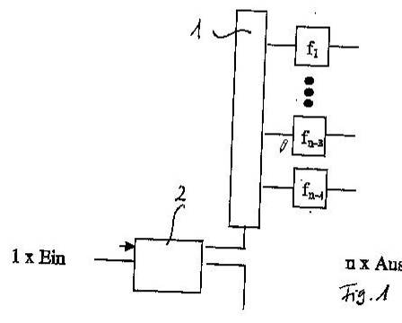
This place covers:
One input frequency is divided in several output frequencies (2 or more)
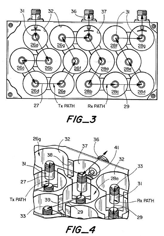
A multiplexer is a network that separates signals from a common port to other ports, sorted according to their frequency. A diplexer is a pair of filters arranged in a three port network, such that a signal at port one will be delivered to port 2 if it is a certain frequency band, and delivered to port 3 if it is in another frequency band.
Duplexer is the term used in radar for the element which separates transmitter and receiver (Section 1.3 Skolnik). However, in the patent literature both terms (diplexer and duplexer) are sometimes confused.
Transmit/receive switching ( in radar systems G01S 7/034; tubes therefor H01J 17/64; waveguide switches H01P 1/10)
Hybrid arrangements, i.e. for transition from single-path two-way transmission to single transmission on each of two path, or vice-versa (multiport networks H03H 7/46; microwave multiplexers H01P 1/213)
Networks for connecting several sources or loads, working on different frequencies or frequency bands, to a common load or source (for use in multiplex transmission systems H04J 1/00)
This place covers:
It is possible that in this group, some dielectric resonators are included because of the relationship between striplines and dielectric resonators (see H01P 1/20309).
This place covers:
Dielectric resonators are also herein included.
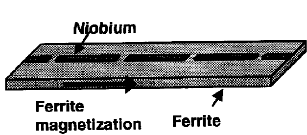
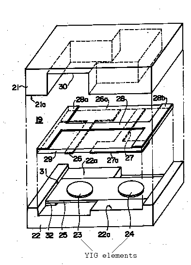
This place covers:
Single crystal yttrium iron garnet (YIG) or gallium-substituted YIG (GaYIG) are magnetic insulators which resonate at a microwave frequency when magnetized by a suitable direct magnetic field.
In this place, the following terms or expressions are used with the meaning indicated:
YIG | Yttrium Iron Garnett |
This place covers:
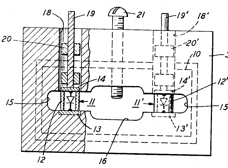
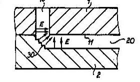
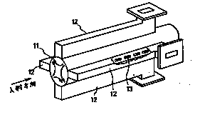
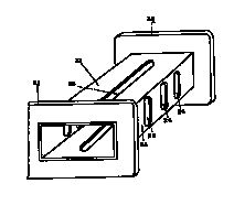
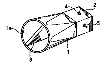
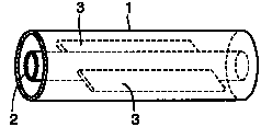
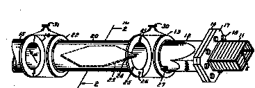
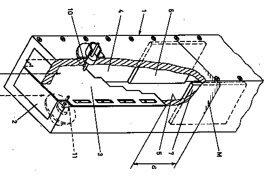
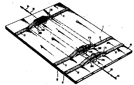
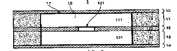
An evanescent mode waveguide may have a conducting tube having an arbitrary cross-sectional shape and having at least one resonator. The dimensions of the cross-section are chosen to allow wave propagation at the operating frequency of interest while causing other frequencies to rapidly decay. A sectional length of an evanescent mode waveguide can be represented as a pi or tee section of inductors whose values are functions of section length, dielectric constant, and guide cross section. A resonant post may be inserted in such a way that it penetrates the broad wall of the evanescent mode waveguide, thereby forming a shunt capacitive element between opposite conducting walls of the guide. The resulting combination of shunt inductance and shunt capacitance forms a resonance.
Evanescent resonators are typically constructed from lengths of below-cutoff (e.g. dispersive) transmission line with the resonators formed by posts, capacitive screws, ridges.
This place covers:
An attenuator is an electronic device that reduces the amplitude or power of a signal without appreciably distorting its waveform.
This place does not cover:
Attenuators with transistors |
Attention is drawn to the following places, which may be of interest for search:
Phase shifters | |
Delay lines |
This place covers:
Devices related to environmental conditions.
H01Q 1/50. Structural association of aerials with earthing switches, lead-in devices or lightning protectors (lead-in devices H01B; lightning protectors, switches H01H)
H01R 24/48 .... for overvoltage protection [N9803]
H01P 1/202... Coaxial filters (cascaded coaxial cavities H01P 1/205)
This place covers:
An RF isolator is a two-port passive device made of magnets and ferrite material which is used to protect other RF components from excessive signal reflection.
Usually, one of the ports of the isolator is grounded.
This place covers:
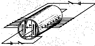
An edge-guided mode device is provided with a dominant mode that resembles TEM energy propagation except that there is a strong transverse field displacement causing the wave energy to be concentrated along the edges of a metal stripline conductor formed on the surface of a ferrite substrate located on a metal ground plane and having a magnetic field applied thereto perpendicular to the ground plane. The edges are designed to be free of abrupt changes in order that there be no abrupt impedance change of the circuit. Non-reciprocal behaviour is obtained by asymmetrically loading the edges.
See documents US3,617,951 and US3,555,459
This place covers:
In this class of isolator, an absorption element (dummy load, dielectric member, ferrite slab, etc...) could be coupled to the isolator in order to absorb the energy of a microwave propagating backwardly.
This place covers:
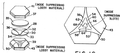
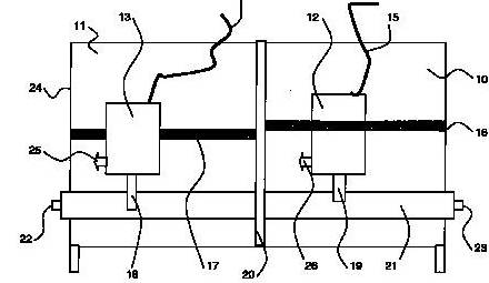
The use of a lossy element in the isolator will produce a change in the field distribution over the conductor (microstrip or transmission line) of the isolator (see figure).
This place covers:
Ferrite circulators are typically configured as multi-port (e.g., three-port) passive RF or microwave devices having within a housing magnets and ferrite material that may be used to control the direction of signal flow in, for example, an RF circuit or a microwave circuit. For example, ferrite circulators may be used to control signal flow in wireless base station or power amplifier applications. Ferrite isolators (see H01P 1/36) also may be constructed by terminating one port of a ferrite circulator. Terminating one port results in signal or energy flow in only one direction, which may be used, for example, for isolating components in a chain of interconnected components.
For more general information about circulators/isolators: http://www.tscm.com/circulat.pdf
This place covers:
Usually, a 3-port circulator is generally called a Y-junction circulator. In case of specification of the circulator, see H01P 1/387 (stripline circulators) or H01P 1/39 (waveguide circulators).
This place does not cover:
Gyrators | |
One way transmission-networks (unilines) |
This place covers:
The Faraday effect is produced when the plane of polarization of incident energy is rotated by passing the energy through an axially oriented, unidirectional, bias magnetic field. This principle is combined with well-known wave-guide principles in determining the propagation paths of electromagnetic energy in the coupler.
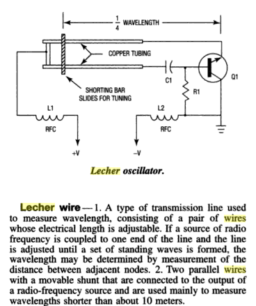
This place covers:
"Waveguide" as applied to transmission lines includes only high-frequency coaxial cables or Lecher lines, and as applied to resonators, delay lines, or other devices includes all devices having distributed inductance and capacitance.
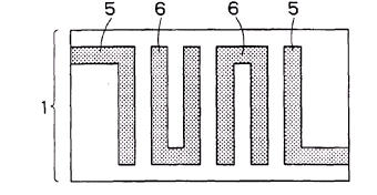
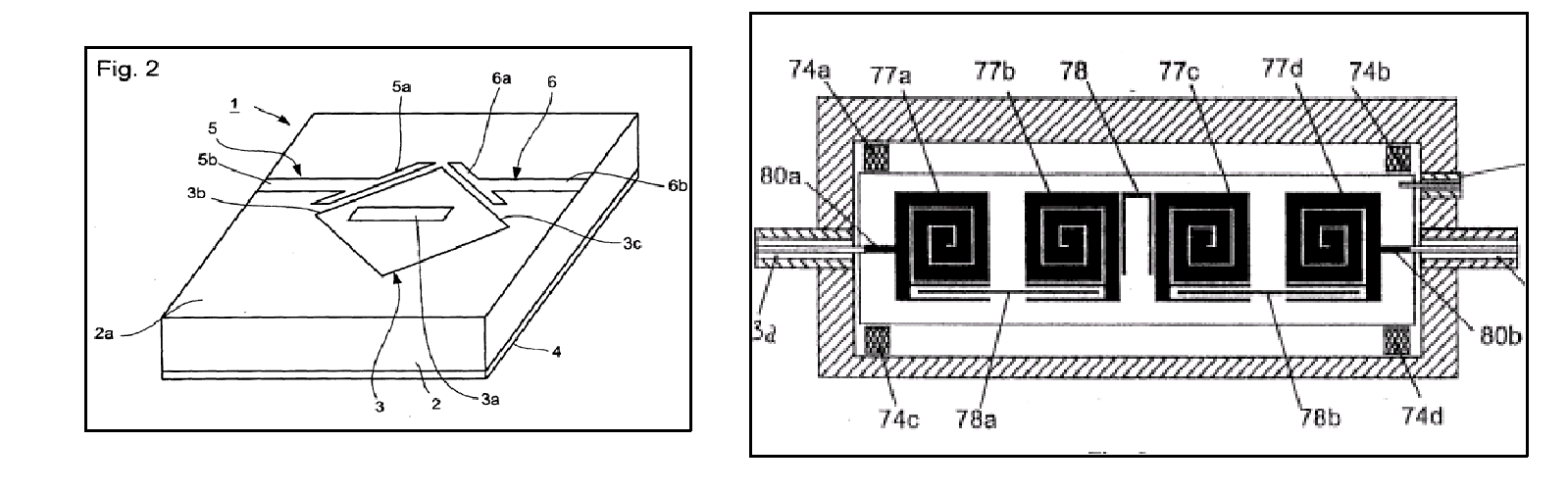
This place covers:
A coplanar waveguide consists of a strip of thin metallic film on the surface of a dielectric slab with two ground electrodes running adjacent and parallel to the strip.
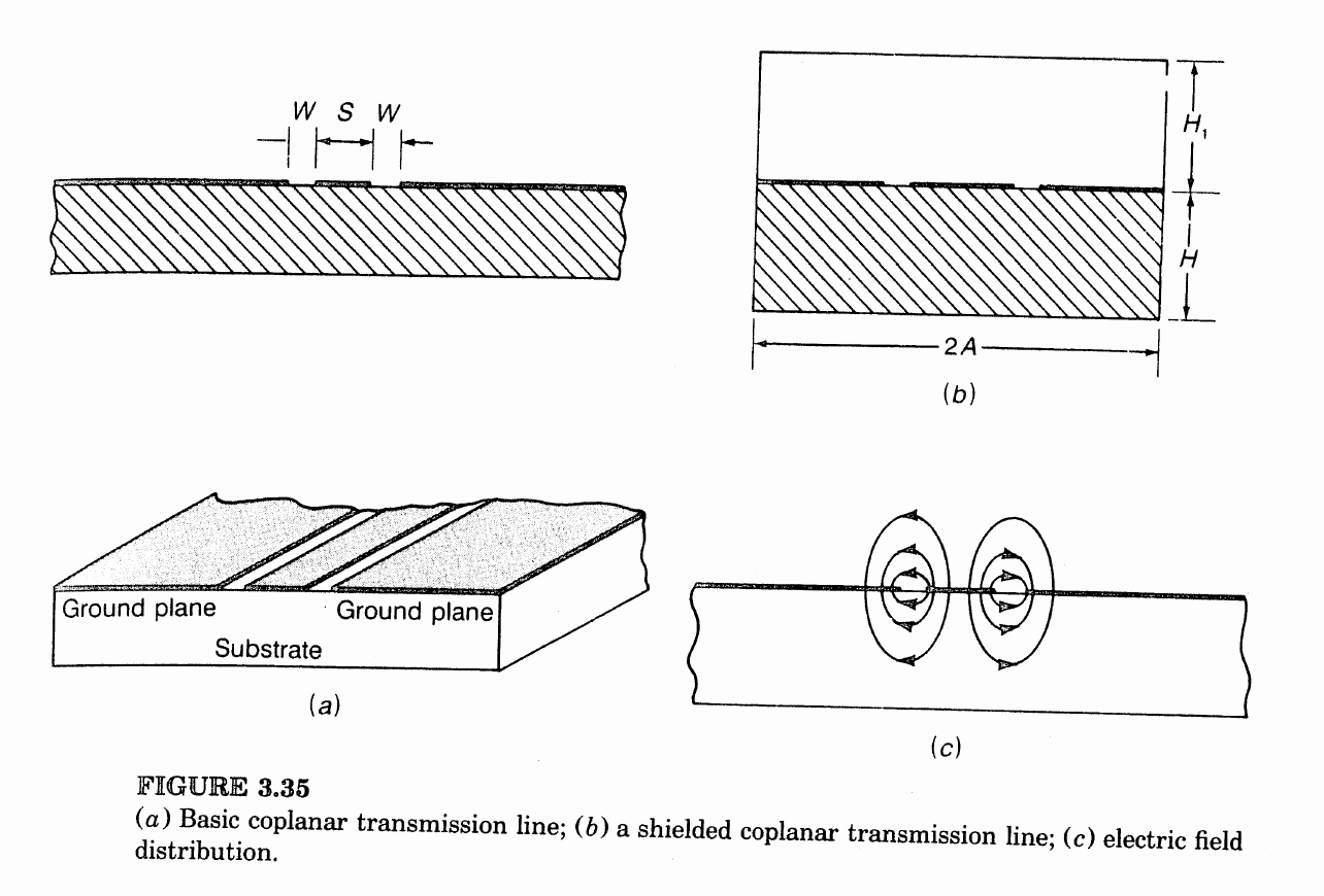
In this place, the following terms or expressions are used with the meaning indicated:
CPW | CoPlanar Waveguide |
This place covers:
Coplanar line including a ground electrode (in addition to the two electrodes of the coplanar line) on the surface opposite to the one where the strip of thin conductor is placed.
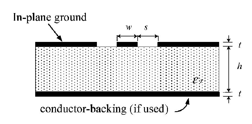
In this place, the following terms or expressions are used with the meaning indicated:
FGC | Finite Ground Coplanar |
CBCPW | Conductor Backed Coplanar Waveguide |
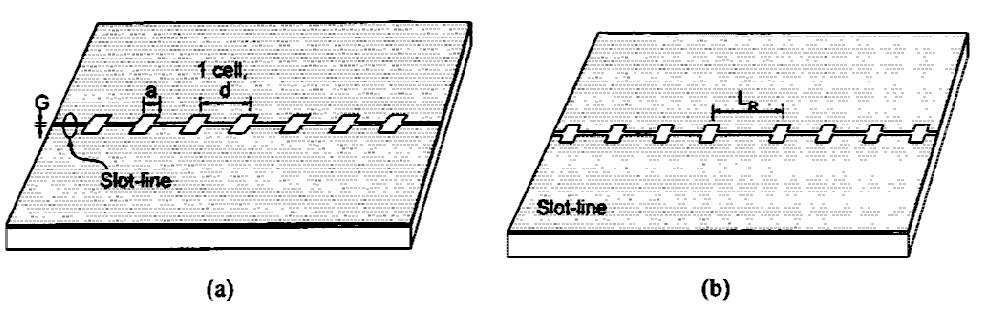
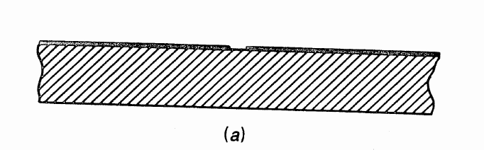
This place covers:
A fin-line is a shielded slot line.
Slot line
Fin-line
This place covers:
The difference between a coplanar stripline and a coplanar line/waveguide is that the coplanar stripline has, at least 2, strip line conductors provided on a substrate and without ground electrodes between them.
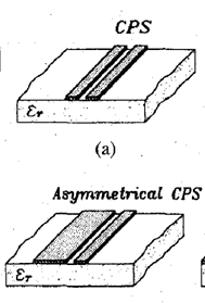
In this place, the following terms or expressions are used with the meaning indicated:
CPS | Coplanar Stripline |
This place covers:
Basically, a high frequency transmission line comprising parallel wires.
Coaxial cable are herein "usually" classified when the resonance frequency is a microwave resonance frequency (above 500 MHz) or there are modes (TEM) involved in the transmission of signals.
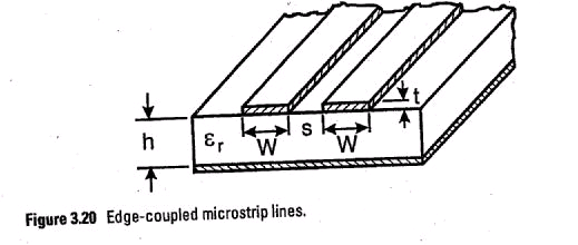
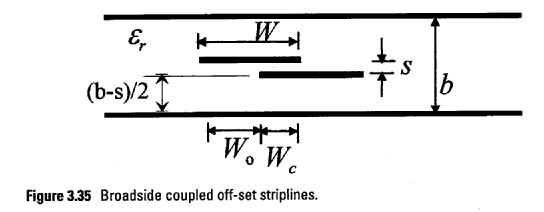
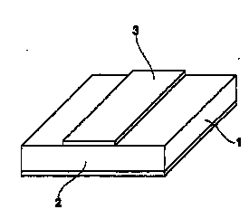
This place covers:
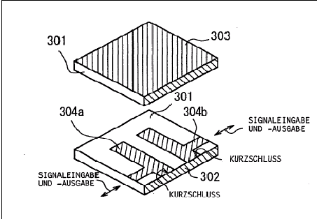
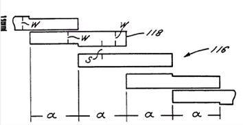
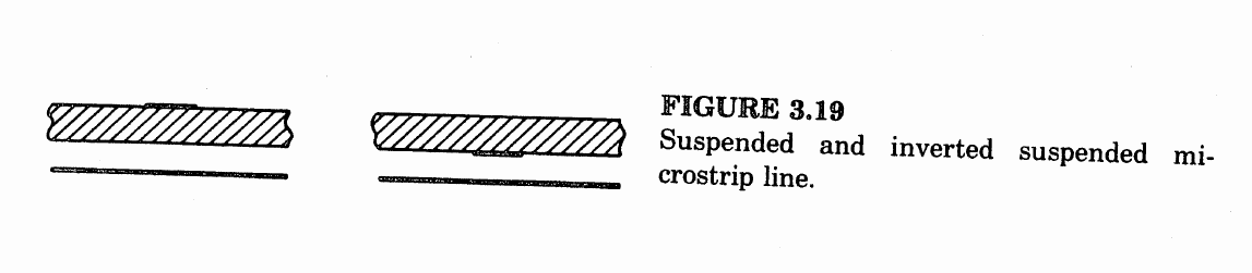
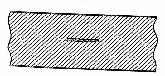
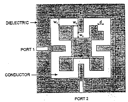
Microstrip: A conductor of width W is printed on a thin, grounded dielectric substrate of thickness d and relative permittivity e.
Stripline: A thin conducting strip of width W is centered between two wide conducting ground planes of separation b, and the entire region between the ground planes is filled with a dielectric.
In patent documents, the following words/expressions are often used as synonyms:
- "microstrip", "stripline", "strip line", "suspended line", "differencial line" and "quasi-coaxial line"
This place covers:
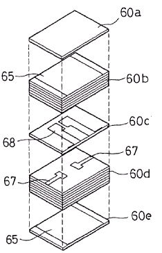
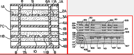
Microstrip line with a plurality of dielectric layers between the conductor line and the ground electrode.
This place covers:
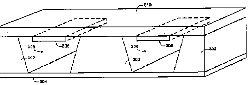
A transmission line circuit is provided in which a layer of material is deposited on a conductive plane. Channels are formed (e.g., by etching) in material such that conductive plane is exposed. Signal traces are formed on a substrate (e.g., by etching the desired pattern in a copper sheet bonded to the substrate) which is then bonded to material such that traces are aligned with channels.
This place covers:
The dielectric provided between the transmission conductor and the ground plane is air or gas.
This place does not cover:
The top and bottom walls are metallized on a substrate and the side walls of the waveguide are implemented with metallized vias or similar metallizations.
Posts or vias are used to delimitated the waveguide in the substrate.
Attention is drawn to the following places, which may be of interest for search:
Printed circuit boards |
In this place, the following terms or expressions are used with the meaning indicated:
SIW | Surface Integrated Waveguide |
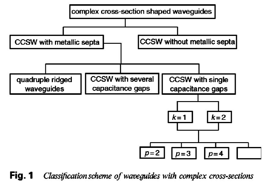
This place covers:
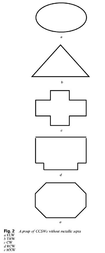
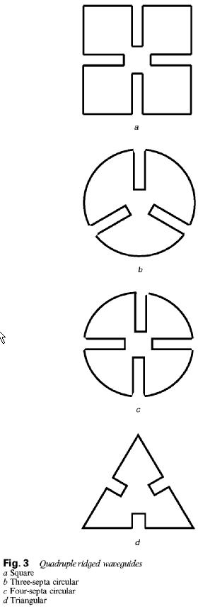
Metallic waveguides comprising a complex cross section.
See XP006017863.
In this place, the following terms or expressions are used with the meaning indicated:
" Trapped mode" | the mode caused by reflections of wave energy between conductive discontinuities in the waveguide on opposite sides of a window member that join two different waveguides. |
"Ghost modes" | Modes associated with resonant modes in the dielectric window itself (see US3594667, column 3, lines 8-26) |
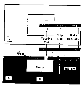
This place covers:
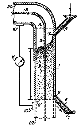
Proposed by Yoneyama and Nishida in 1981, non-radiative (NRD) guide circuit is nowadays a well-known technology for millimeter-wave applications. Its basic component, the NRD waveguide, consists of a rectangular section dielectric rod (height α, width 2w, permittivity εr), sandwiched between conductiong plates that are at a distance apart less than half the free space wavelength λ0: thus, all discontinuities that maintain appropriate symmetry become purely reactive, with the advantage of a strong reduction in interference and radiation problems in integrated circuits. The same waveguiding structure, but with a larger space between the plates, was already proposed in 1953 by Tischer with a view to obtaining an ultra-low-loss waveguide, know as H guide. In this situation the non radiation condition α < λ0/2 is no linger maintained and the structure suffers the drawback of undesirable radiation effects from discontinuities.
See GB2360139, US-A-4028643, US-A-4463330, US-4677404.
Attention is drawn to the following places, which may be of interest for search:
The H-guide, precursor of the NRD |
In patent documents, the following abbreviations are often used:
NRD | Non-radiating dielectric waveguide (see H01P 3/165) |
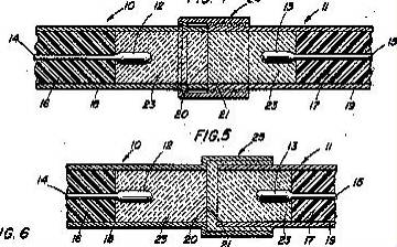
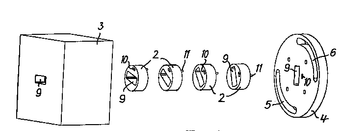
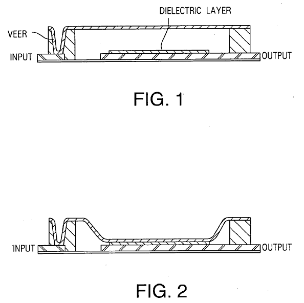
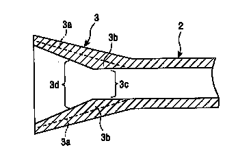
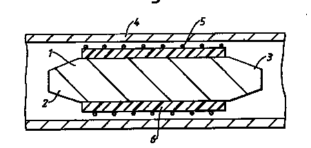
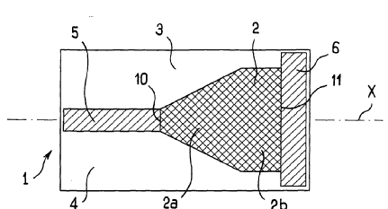
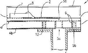
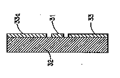
This place covers:
The original NRD patent: JP57166701
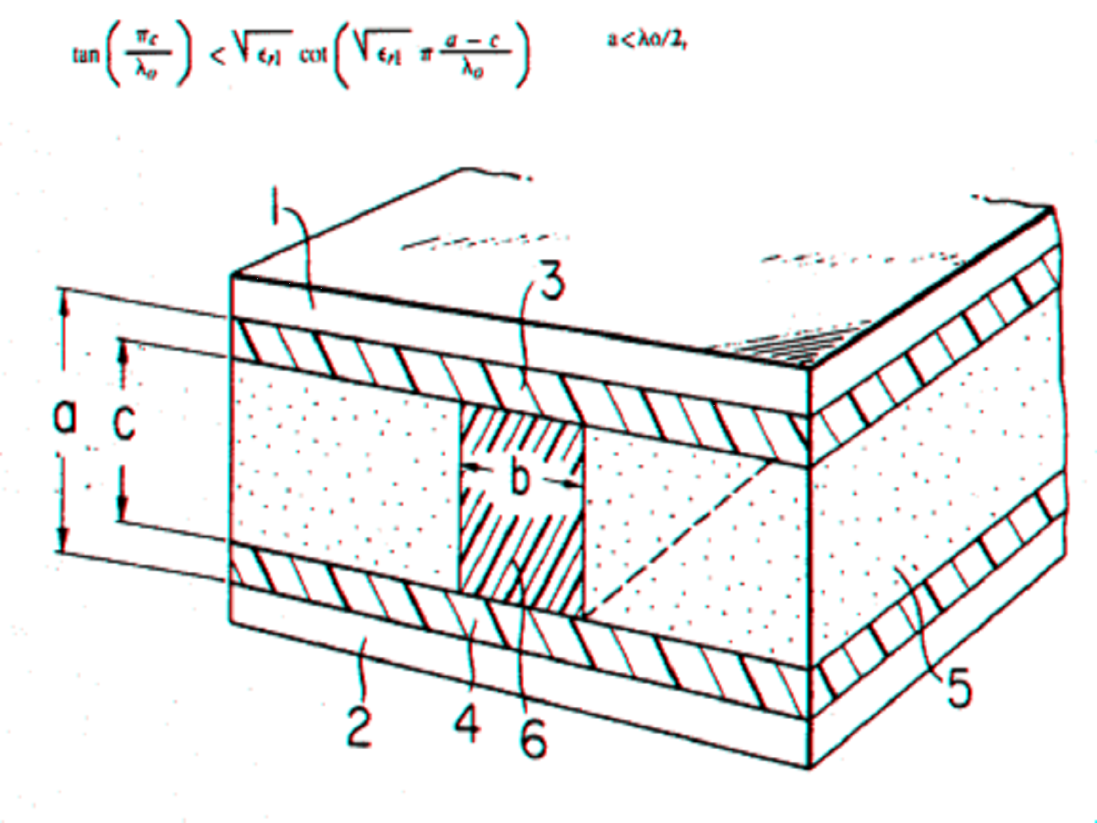
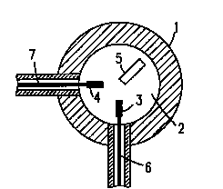
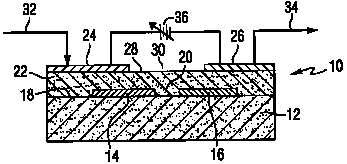
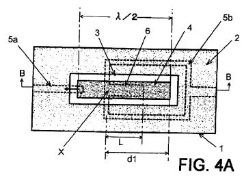
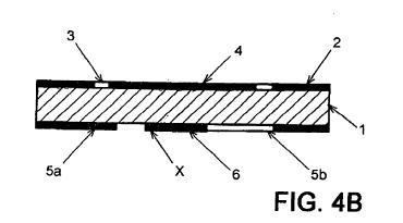
In this figure, 1 and 2 are metal layers, 3 and 4, dielectric layers and 6 is a low loss high dielectric constant dielectric.
Sometimes the term non-radiative is misspelled as "non-radioactive".
Attention is drawn to the following places, which may be of interest for search:
Amplifiers with coupling networks | H03F 3/60, H03F 3/602, H03F 3/604 (with FET's) |
H03H 7/38, H10W 44/00 (Related to impedance arrangements).
H01R 24/40 (coaxial connectors) and the Keyword "wadded wire contact".
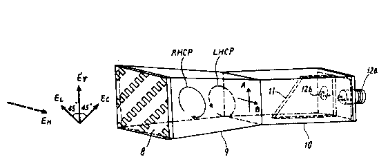
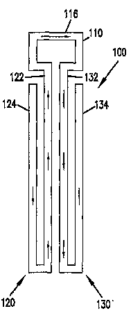
This place covers:
Balun: Device which transforms a balanced input transmission signal to unbalanced output signals, are widely used in many application, such as balanced push pull amplifiers (H03H), antenna feed networks (H01Q) and double-balanced mixers.
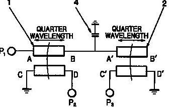
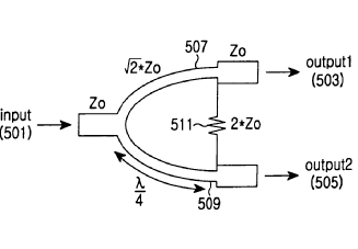
Marchand Balun: see IMDT XP001178439
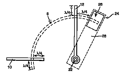
The Marchand balun (see figure below) includes a first line having a length that is one half of a wavelength corresponding to an operating frequency, a second line and a third line each having a length that is one quarter of the wavelength corresponding to the operating frequency, an input terminal connected to one end of the first line, an output terminal connected to one end of the second line, and an output terminal connected to one end of the third line. The output terminals operate in pair as differential output terminals.
Phase inverters in H03H 7/42.
In this place, the following terms or expressions are used with the meaning indicated:
Balun, symetriseur | Balance-Unbalanced coupling device |
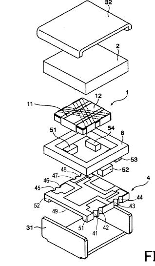
This place covers:
SMT (surface mount technology)
H01P 7/065: when it is referring to a waveguide cavity in the PCB.
Look also in:
H01P 1/161: sustaining two independent orthogonal modes, e.g. orthomode transducer (combining or separating polarisations and frequencies H01P 1/2131)
H01P 1/17: for producing a continuously rotating polarisation, e.g. circular polarisation
This place covers:
Reference document: E. Wilkinson: "An N-way Hybrid Power divider", IEEE Trans., vol. MTT-8, pp 116-118
H03H 7/185 Multiple networks...comprising distributed impedance elements together with lumped impedance elements.
In this place, the following terms or expressions are used with the meaning indicated:
Wilkinson power divider | N-way power divider that splits the input power into output power at N ports and that also provides isolationbetween the output powers. |
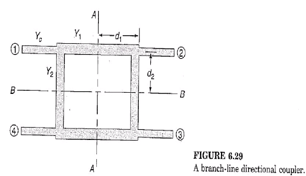
This place covers:
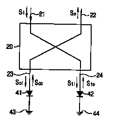
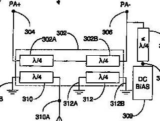
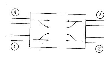
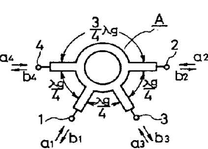
Directional couplers are four-port circuits where one port is isolated from the input port. All four ports are (ideally) matched, and the circuit is (ideally) lossless.
What do we mean by "directional"? A directional coupler has four ports, where one is regarded as the input, one is regarded as the "through" port (where most of the incident signal exits), one is regarded as the coupled port (where a fixed fraction of the input signal appears, usually expressed in dB), and an isolated port, which is usually terminated. If the signal is reversed so that it enter the "though" port, most of it exits the "input" port, but the coupled port is now the port that was previously regarded as the "isolated port". The coupled port is a function of which port is the incident port.
Looking at the generic directional coupler schematic above, if port 4 is the incident port, port 3 is the transmitted port (because it is connected with a straight line). Either port 1 or port 2 is the coupled port, and the other is the isolated port, depending on whether the coupling mode is forward or backward.
This place covers:
The couplers can be divided depending on the coupling between the lines (see following classification)
It can be a weak coupling:
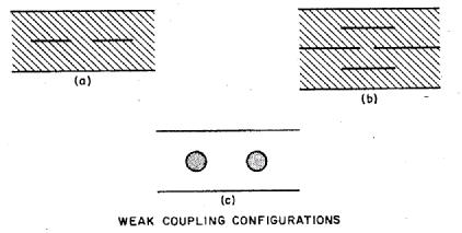
or a tight coupling (couping <= 3 dB)
This place covers:
Weak coupling is associated with edge coupling (except Lange couplers (see H01P 5/186)).
This place covers:
Lange couplers are generally used to couple electromagnetic energy between transmission lines. In a four port hybrid, there is an input port and a direct port, these two ports being directly and conductively connected to each other, as well as a coupled port, the latter being connected to transmission lines coupled electromagnetically (inductively and capacitively) to the conductors extending between the input and direct ports.
In a Lange type coupler, each strip conductor is divided into mutually parallel sections, and the conductor sections from the two different strip conductors are interdigitated, so that each strip section is located between two sections from the other conductor. In a planar arrangement, it is necessary to have cross-over connectors in order to establish a direct conductive connection between the various sections extending in parallel.
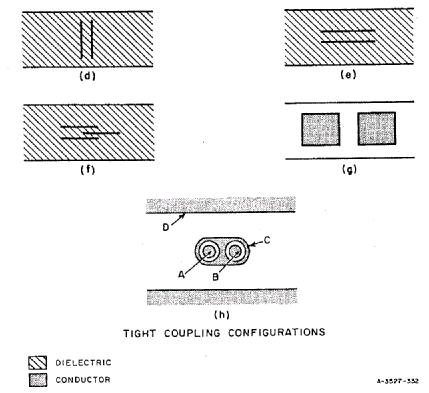
This place covers:
Tight coupling is generally associated with broadband coupling.
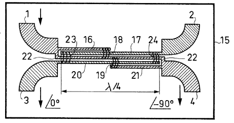
This place covers:
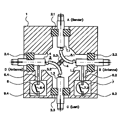
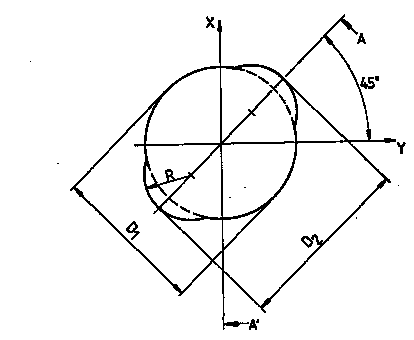
The magic-T is a combination of the H-type and E-type T junctions.
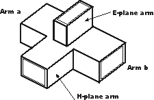
Magic T waveguide junction
The diagram above depicts a simplified version of the Magic T waveguide junction with its four ports.
To look at the operation of the Magic T waveguide junction, take the example of when a signal is applied into the "E plane" arm. It will divide into two out of phase components as it passes into the leg consisting of the "a" and "b" arms. However no signal will enter the "H plane" arm as a result of the fact that a zero potential exists there - this occurs because of the conditions needed to create the signals in the "a" and "b" arms. In this way, when a signal is applied to the H plane arm, no signal appears at the "E plane" arm and the two signals appearing at the "a" and "b" arms are 180° out of phase with each other.
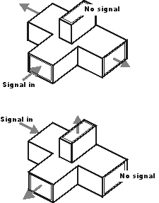
Magic T waveguide junction signal directions
When a signal enters the "a" or "b" arm of the magic T waveguide junction, then a signal appears at the E and H plane ports but not at the other "b" or "a" arm as shown.
Attention is drawn to the following places, which may be of interest for search:
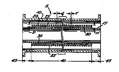
Cavity resonators |
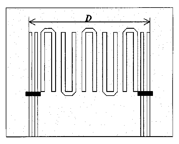
This place covers:
The basic structure of a microstrip line resonator consists of a ground electrode formed on one surface of a dielectric plate and a microstrip line electrode formed on the other surface.
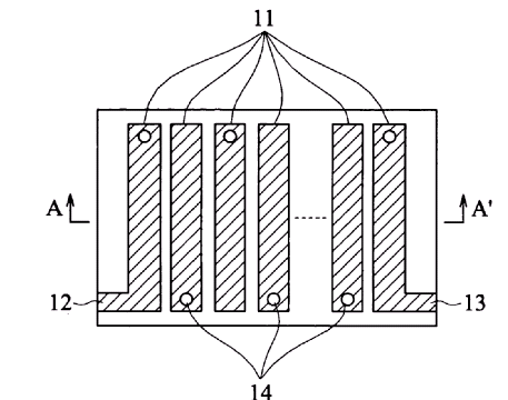
Microstrip line having four self-resonant spiral resonators on a dielectric structure.
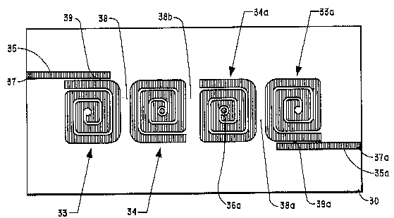
The microstrip ring resonator may be any strip of circular, elliptic or quadrate shape.
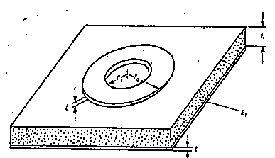
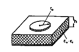
A rectangular micostrip disk can be considered as a degenerated microstrip line having line-width w and line-area π*ro2
The microstrip loop resonator A consists of a meander loop of four identical arms (each of which may be taken as a meander line).
The microstrip loop resonator B includes an open conductive loop with folded transmission line segments extending from the adjacent ends of the loop formed on dielectric substrate.
The hairpin resonator disposes a substrate of finite thickness is embedded inside a shielding box and is used as support for the metallized plane.
In patent documents, the following words/expressions are often used as synonyms:
- "stripline" and "strip line resonator"
This place covers:
Dielectric structure in which ground conductors share the same plane defined by the conductor.
Coplanar resonator formed with a conductor ground plane provided on the opposite side of the dielectric.
This place covers:
The tunable resonator shown below, includes a resonator coil and a variable capacitance portion. The variable capacitance portion tunes the tunable resonator.
This place covers:
Delay equalization corresponds to adjusting the relative phases of different frequencies to achieve a constant group delay.
Attention is drawn to the following places, which may be of interest for search:
Shaping pulses with delay elements (lines) |
Attention is drawn to the following places, which may be of interest for search:
Manufacture of coaxial cable | |
Manufacturing of antennas | H01Q 15/141 and subgroups, H01Q 13/0283, H01Q 21/0087 |
Attention is drawn to the following places, which may be of interest for search:
Optical waveguides |
Attention is drawn to the following places, which may be of interest for search:
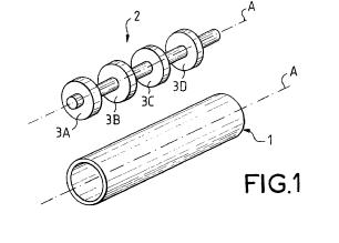
Manufacturing tubes | B21C 37/15 and subgroups |
In patent documents, the following words/expressions are often used as synonyms:
- "etching", "manufacturing", " deposition" and "sputtering"