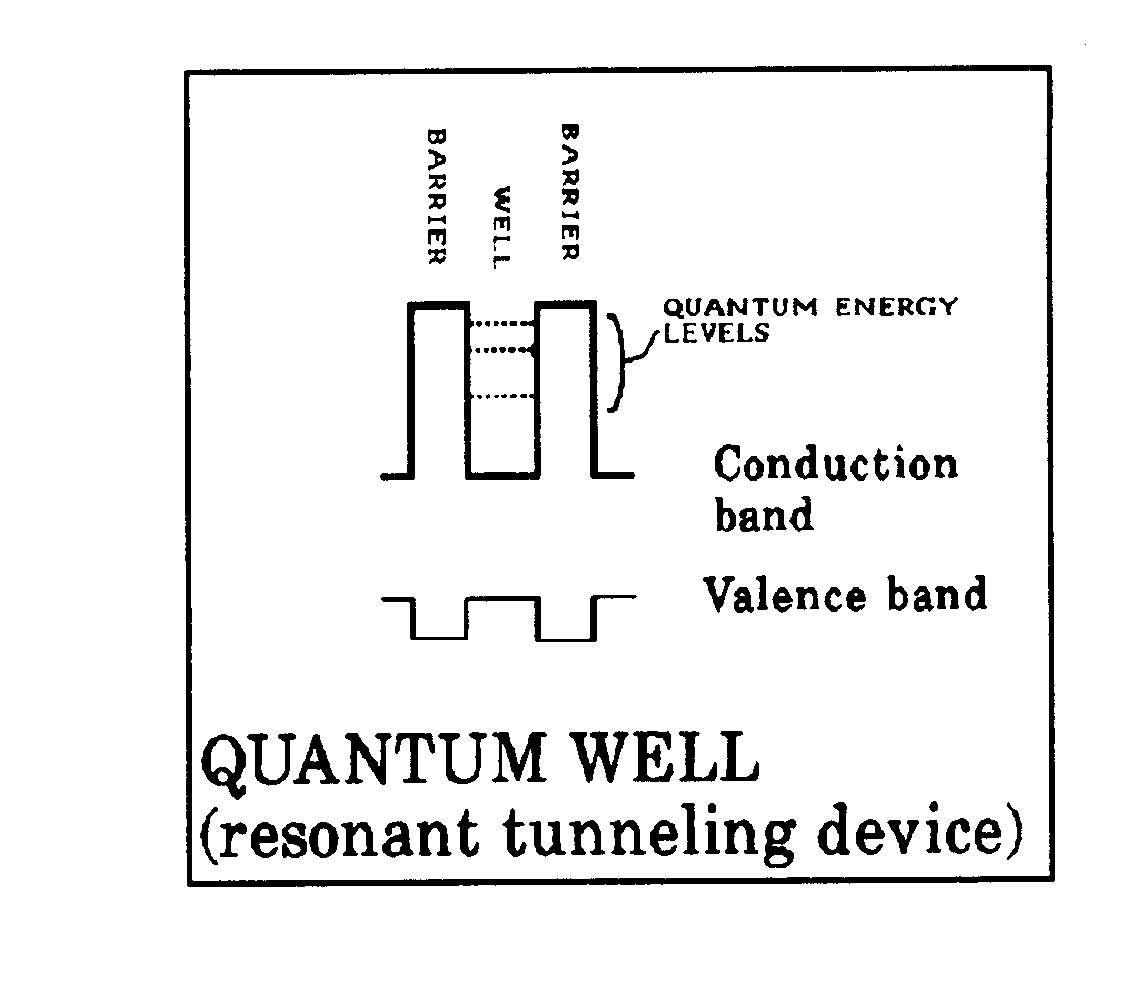
| | This subclass is indented under the class definition. Subject matter wherein the active solid-state device is
provided with one or more electrical contacts or leads.
SEE OR SEARCH THIS CLASS, SUBCLASS:
| 41, | for point contact rectifiers. |
| 44, | through 47, for devices with a metal contact alloyed
to elemental semiconductor type PN junction in a non-regenerative
structure. |
| 54, | for Schottky barrier to amorphous semiconductor
material device. |
| 73, | for Schottky barrier to polycrystalline semiconductor
material device. |
| 81, | and 82, for light emitter combined with or also
constituting a light responsive device and having a specific housing
or contact structure. |
| 91, | for plural light emitting devices with shaped contacts
or opaque masking. |
| 99, | for light emitting devices with specified housing
or contact structure. |
| 145, | for a regenerative type device combined with a FET
with extended latching current level and a low impedance channel
contact extending below the device surface. |
| 155, | and 156, for a regenerative type device with switching
speed enhancing means (e.g., a Schottky contact). |
| 177, | through 182, for a regenerative type device with
housing or external electrode. |
| 217, | for a majority signal carrier charge transfer device
with a conductive means in direct contact with channel (e.g., a
non-insulated gate). |
| 260, | for JFET having the same channel controlled by,
for example, Schottky barrier and pn junction gates. |
| 276, | for a JFET in a microwave integrated circuit with
a contact or heat sink extending through a hole in the semiconductor. |
| 280, | through 284, for JFETs with a Schottky gate electrode. |
| 316, | through 322, for a variable threshold insulated
electrical field effect device with additional contacted control
electrode. |
| 343, | for graded channel dopant IGFET device with plural
sections connected in parallel and having all contacts on the same
surface. |
| 382, | through 385, for an IGFET in an integrated circuit
with a refractory material contact to source or drain region. |
| 449, | through 457, for Schottky contacts in light responsive
devices. |
| 471, | through 486, for Schottky contact devices. |
| 502, | for high power integrated circuit devices with electrical
isolation and a backside collector contact. |
| 503, | for an integrated circuit device with electrically
isolated components having a contact or metallization configuration
to reduce parasitic coupling. |
| 522, | for beam-lead supported semiconductor islands in
integrated circuits. |
| 573, | for Darlington configuration non-isolated bipolar
transistors with resistance means connected between transistor base
regions and with housing or contact structure or configuration. |
| 576, | for complementary bipolar transistors sharing a
common active region (e.g., IIL, I2L) including
lateral bipolar transistor structure and having contacts of a refractory
material. |
| 584, | for bipolar transistor device with enlarged emitter
area and with housing or contact means. |
| 602, | for a voltage variable capacitance device with specified
housing or contact. |
| 621, | for a semiconductor device with electrical contact
in a hole in the semiconductor (e.g., lead extends through semiconductor
body). |
| 624, | for mesa structure device having a low resistance
ohmic connection along a mesa edge. |
| 661, | through 663, for superconductive contacts or leads. |
| 664, | for transmission line leads. |
| 665, | for contacts or leads including fusible link or
noise suppression means. |
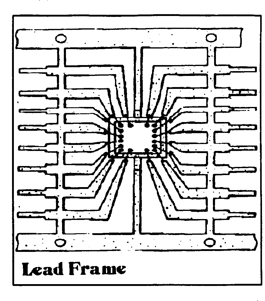
| 666, | through 677, for lead frames. |
| 688, | and 689, for housings with large area flexible electrodes
in press contact with opposite sides of active semiconductor chip
and surrounded by an insulating element. |
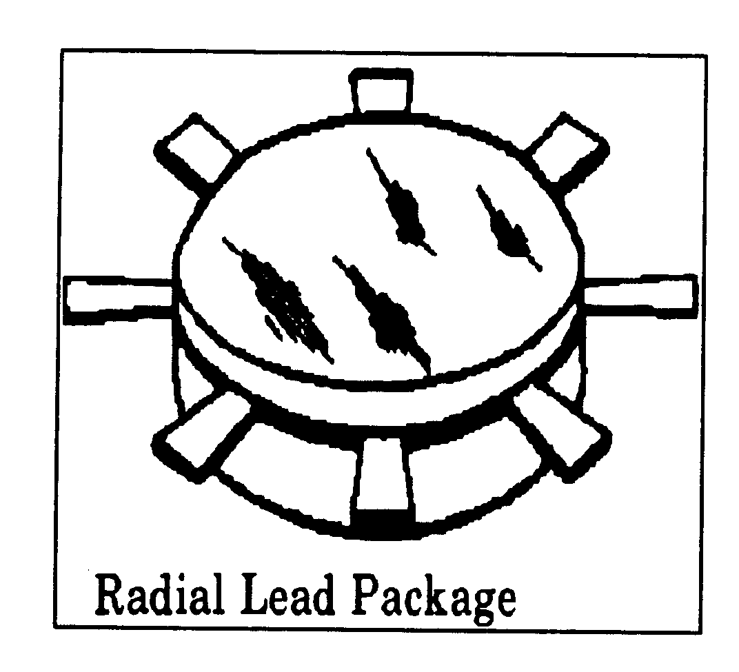
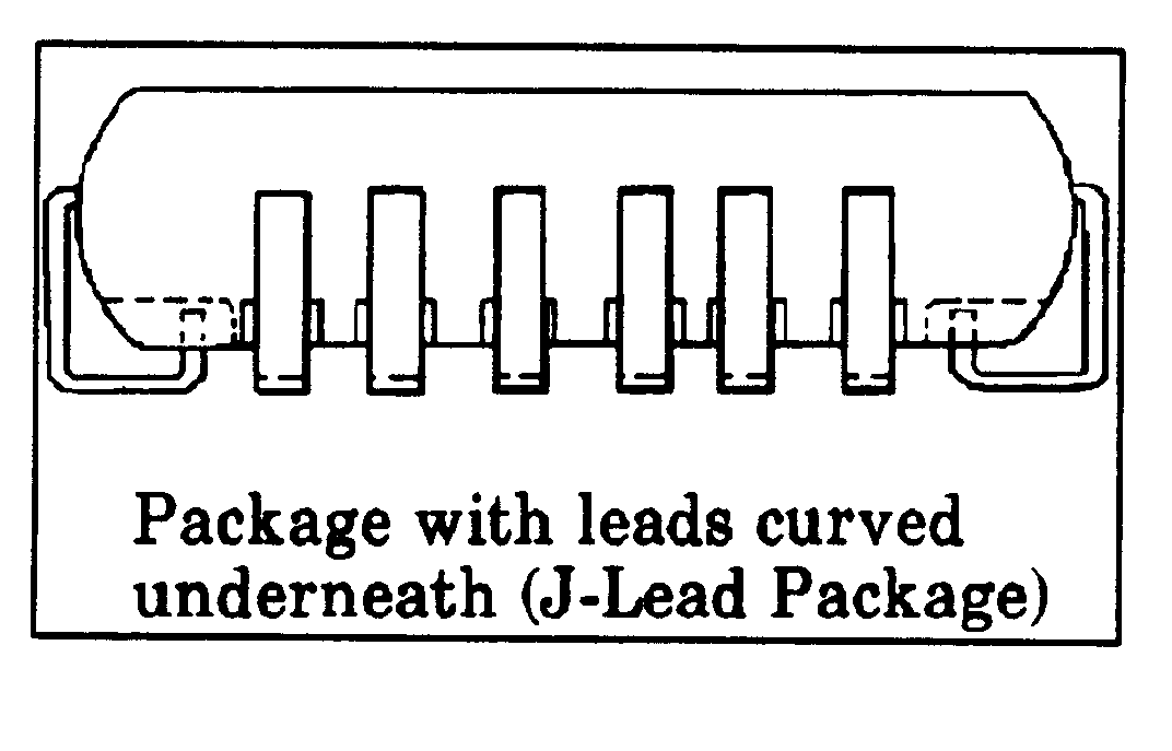
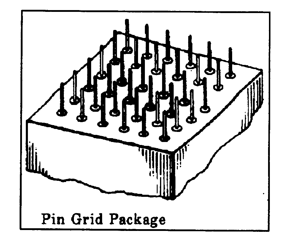
| 690, | through 700, for housings with specified contact
or lead. |
| 905, | for plural DRAM cells sharing a common contact or
common trench. |
| 926, | for a device with an elongated lead extending axially
through another elongated lead. |
| 928, | for shorted pn or Schottky junction other than an
emitter junction. |
SEE OR SEARCH CLASS:
| 174, | Electricity: Conductors and Insulators,
subclasses 99+ for bus bar structure, per se. |
| 361, | Electricity: Electrical Systems and Devices,
subclasses 772 through 776for specific lead configurations connecting electronic
systems and devices to printed circuit boards. |
|