| CPC H03K 17/6871 (2013.01) [H01L 29/2003 (2013.01); H01L 29/7786 (2013.01)] | 20 Claims |
|
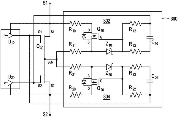
1. Apparatus for performing substrate voltage management, comprising:
an active substrate voltage management circuit configured to be coupled to a substrate of a bidirectional gallium nitride high electron mobility transistor comprising a first source and a second source,
wherein the active substrate voltage management circuit comprises a first circuit that is connected to the first source and a second circuit that is connected to the second source such that when the bidirectional gallium nitride high electron mobility transistor is operational one of the first circuit or the second circuit connects one of the first source to the substrate or the second source to the substrate, respectively, to control a bias voltage applied to the substrate, and
wherein a first resistor of the first circuit and a second resistor of the second circuit are connected in parallel to each other and the substrate to protect a first transistor of the first circuit and a second transistor of the second circuit from an overcurrent situation when the first transistor and the second transistor are both on together and when the bidirectional gallium nitride high electron mobility transistor device is not.
|