| CPC H01L 31/1804 (2013.01) [H01L 21/0275 (2013.01); H01L 21/3046 (2013.01); H01L 21/3086 (2013.01); H01L 21/30621 (2013.01); H01L 21/486 (2013.01); H01L 21/6835 (2013.01); H01L 21/76898 (2013.01); H01L 23/49827 (2013.01); H01L 31/1892 (2013.01); H01L 2221/68345 (2013.01); Y02E 10/547 (2013.01)] | 20 Claims |
|
1. A method for substrate structuring, comprising:
bonding a silicon substrate to a carrier plate via an adhesive, the substrate having a thickness between 110 μm and 300 μm, the adhesive comprising at least one of a water-soluble adhesive layer, a solvent-soluble adhesive layer, a thermal release adhesive layer, or a UV release adhesive layer;
chucking the carrier plate and the silicon substrate on a support stand;
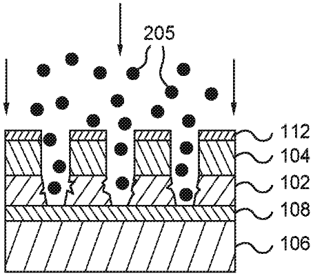
patterning the substrate to form one or more cavities and one or more vias therein, the one or more cavities and the one or more vias having different morphologies; and
exposing the substrate to an etch process to remove debris from the one or more cavities and the one or more vias, the etch process further smoothening one or more surfaces of the substrate.
|