| CPC H01L 31/109 (2013.01) [H01L 31/028 (2013.01); H01L 31/02327 (2013.01); H01L 31/105 (2013.01); H01L 31/1804 (2013.01)] | 22 Claims |
|
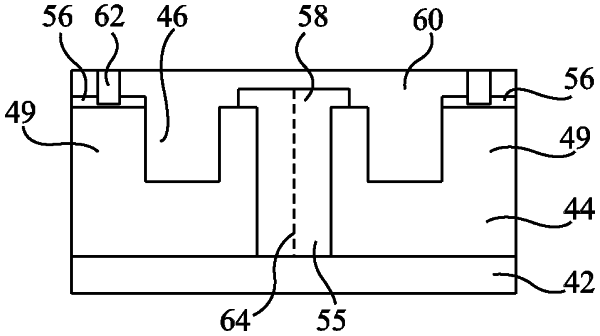
1. A method, comprising:
etching first and second trenches in a layer of semiconductor material to delimit a central region of semiconductor material, wherein the layer of semiconductor material is located on a first layer of insulating material;
depositing a second layer of insulating material which fills the first and second trenches and covers the central region;
etching the second layer of insulating material and the layer of semiconductor material at the central region to form a cavity which extends completely through both the second layer of insulating material and the layer of semiconductor material to reach the first layer of insulating material and delimit a first portion of the central region and a second portion of the central region spaced apart from each other by said cavity; and
epitaxially growing a semiconductor material different than a semiconductor material of said layer of semiconductor material in said cavity to form an active area of a photodiode.
|