| CPC H01L 29/7832 (2013.01) [H01L 29/66893 (2013.01); H01L 29/7825 (2013.01)] | 20 Claims |
|
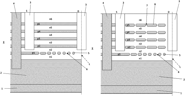
1. A semiconductor device, comprising:
a substrate of a first conductivity type that is a base for the semiconductor device;
a high voltage junction field effect transistor, JFET, over the substrate, wherein the JFET comprising a plurality of parallel conductive layers, the JFET being isolated with a deep polycrystalline trench of a first conductivity type on a source side of the JFET;
a first conductive layer of the second conductivity type of the parallel conductive layers stretching over the substrate;
wherein on top of the first conductive layer of the second conductivity type is arranged a plurality of layers forming the parallel conductive layers with channels formed by a plurality of doped epitaxial layers of the second conductivity type with a plurality of gate layers of the first conductivity type on both sides thereof;
wherein,
a lowermost layer of the first conductivity type is arranged in the form of consecutive dots with different lengths and distances between them.
|