US 11,837,652 B2
Semiconductor processing system with in-situ electrical bias and methods thereof
David Hurley, Dublin (IE); Ioan Domsa, Dublin (IE); Ian Colgan, Dublin (IE); Gerhardus Van Der Linde, Dublin (IE); Patrick Hughes, Dublin (IE); Maciej Burel, Dublin (IE); Barry Clarke, Dublin (IE); Mihaela Ioana Popovici, Haasrode (BE); and Lars-Ake Ragnarsson, Heverlee (BE)
Assigned to TOKYO ELECTRON LIMITED, Tokyo (JP)
Filed by Tokyo Electron Limited, Tokyo (JP)
Filed on May 9, 2022, as Appl. No. 17/662,579.
Application 17/662,579 is a division of application No. 16/841,342, filed on Apr. 6, 2020, granted, now 11,335,792.
Prior Publication US 2022/0262921 A1, Aug. 18, 2022
Int. Cl. H01L 29/66 (2006.01); H01L 21/02 (2006.01); H01L 21/67 (2006.01)
CPC H01L 29/6684 (2013.01) [H01L 21/02532 (2013.01); H01L 21/02554 (2013.01); H01L 21/02667 (2013.01); H01L 21/67098 (2013.01)] 20 Claims
OG exemplary drawing
 
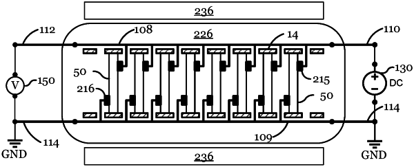
1. A system for processing semiconductor wafers, the system comprising:
a processing chamber;
a substrate holder configured to support a semiconductor wafer;
a heating element configured to heat the semiconductor wafer supported by the substrate holder;
a first electrode configured to be detachably attached to a first major surface of the semiconductor wafer;
a first wire coupling the first electrode to a first potential node; and
a load-rail configured to detachably attach the first electrode to the first major surface of the semiconductor wafer and load the semiconductor wafer into the processing chamber.