| CPC H01L 29/4238 (2013.01) [H01L 21/823418 (2013.01); H01L 21/823431 (2013.01); H01L 21/823468 (2013.01); H01L 21/823475 (2013.01); H01L 23/5226 (2013.01); H01L 27/0886 (2013.01); H01L 29/41775 (2013.01); H01L 29/7851 (2013.01)] | 19 Claims |
|
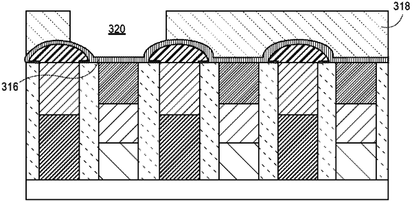
1. An integrated circuit structure, comprising:
a plurality of gate structures above substrate, each of the gate structures including a gate insulating layer thereon, the gate insulating layer having an uppermost surface;
a plurality of conductive trench contact structures alternating with the plurality of gate structures, each of the conductive trench contact structures including a metal oxide cap structure thereon, the metal oxide cap structure having an uppermost surface above the uppermost surface of the gate insulating layer;
a plurality of dielectric spacers alternating with the plurality of gate structures and the plurality of conductive trench contact structures, wherein an uppermost surface of the plurality of dielectric spacers is at a same level as an uppermost surface of the plurality of conductive trench contact structures;
an interlayer dielectric material over the plurality of gate structures and over the plurality of conductive trench contact structures;
an opening in the interlayer dielectric material and in a gate insulating layer of a corresponding one of the plurality of gate structures; and
a conductive via in the opening, the conductive via in direct contact with the corresponding one of the plurality of gate structures, and the conductive via on a portion of one or more of the metal oxide cap structures.
|