| CPC H01L 29/063 (2013.01) [H01L 21/046 (2013.01); H01L 29/0623 (2013.01); H01L 29/1095 (2013.01); H01L 29/66068 (2013.01); H01L 29/66734 (2013.01); H01L 29/7397 (2013.01); H01L 29/7811 (2013.01); H01L 29/7813 (2013.01); H01L 29/0615 (2013.01); H01L 29/0619 (2013.01); H01L 29/0696 (2013.01); H01L 29/0878 (2013.01); H01L 29/1037 (2013.01); H01L 29/1608 (2013.01)] | 21 Claims |
|
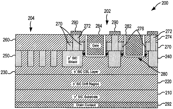
1. A method of forming a semiconductor device, the method comprising:
forming a wide band-gap semiconductor drift region on a substrate, the drift region and the substrate each doped with dopants having a first conductivity type;
implanting second conductivity type dopants into an upper surface of the drift region to form a termination structure in a termination region of the semiconductor device and a shielding pattern in an active region of the semiconductor device, the second conductivity type being opposite the first conductivity type;
forming a first conductivity type semiconductor layer on the upper surface of the drift region via epitaxial growth, the semiconductor layer having a first conductivity dopant concentration of less than 1×10¹⁶/cm3 in the completed semiconductor device; and
implanting second conductivity type dopants into the semiconductor layer in the active region to form well regions of the second conductivity type.
|