| CPC H01L 23/66 (2013.01) [H01L 21/4853 (2013.01); H01L 21/4857 (2013.01); H01L 21/565 (2013.01); H01L 21/568 (2013.01); H01L 21/6835 (2013.01); H01L 23/3128 (2013.01); H01L 23/5383 (2013.01); H01L 23/5386 (2013.01); H01L 23/5389 (2013.01); H01L 24/19 (2013.01); H01L 24/20 (2013.01); H01Q 1/2283 (2013.01); H01L 2221/68372 (2013.01); H01L 2223/6627 (2013.01); H01L 2223/6677 (2013.01); H01L 2224/214 (2013.01)] | 20 Claims |
|
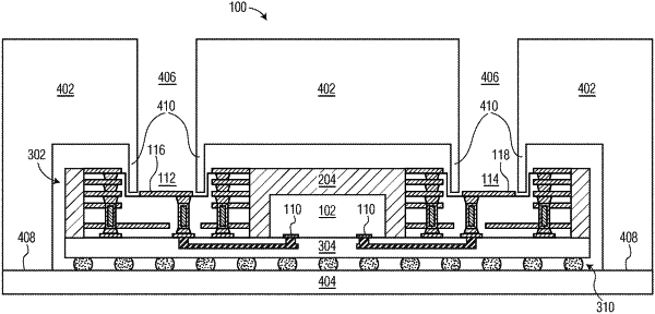
1. A method of manufacturing a semiconductor device, the method comprising:
forming an assembly comprising:
placing a semiconductor die and a launcher structure on a carrier substrate, the launcher structure including an antenna launcher;
encapsulating at least a portion of the semiconductor die and the launcher structure;
applying a redistribution layer on a first major surface of the semiconductor die and a first major surface of the launcher structure, a bond pad of the semiconductor die connected by way of the redistribution layer to the antenna launcher;
attaching the assembly to a substrate; and
attaching a waveguide structure to the substrate, the waveguide structure overlapping the assembly and physically decoupled from the assembly.
|