| CPC G06F 1/1647 (2013.01) [G09F 9/3026 (2013.01); H01L 23/552 (2013.01); H01L 33/62 (2013.01)] | 6 Claims |
|
1. An display apparatus comprising:
a cabinet; and
an LED module assembly detachably disposed in the cabinet;
wherein the LED module assembly comprises:
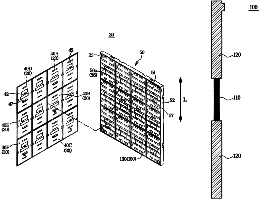
a plurality of LED modules;
a support frame on which the plurality of LED modules are disposed; and
a coupling member configured to couple the plurality of LED modules to the support frame and to include a conductive region,
wherein the plurality of LED modules comprises a corresponding surface facing the support frame and a plating processing region formed along an edge of the corresponding surface,
wherein the coupling member comprises a non-conductive region alternately provided with the conductive region, and
wherein the plating processing region contact the conductive region of the coupling member to attenuate electromagnetic waves generated from the LED module assembly.
|