| CPC H10N 70/841 (2023.02) [H10B 63/00 (2023.02); H10N 70/021 (2023.02); H10N 70/063 (2023.02); H10N 70/8833 (2023.02)] | 17 Claims |
|
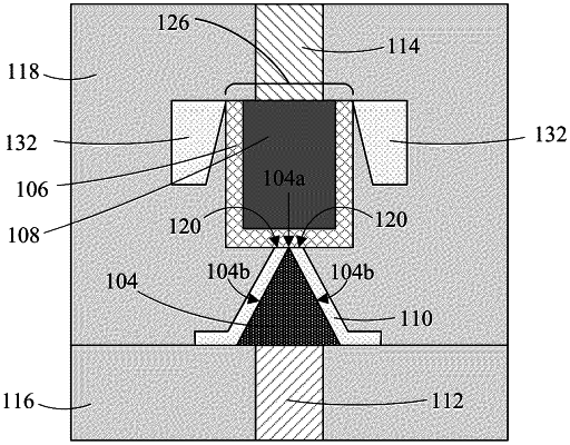
1. A memory device comprising:
a first electrode having tapered sides that converge at a top of the first electrode;
a dielectric layer disposed on and conforming to the tapered sides of the first electrode;
a resistive layer in contact with the top of the first electrode and the dielectric layer; and
a second electrode disposed on the resistive layer, wherein the resistive layer conforms to a bottom and side surfaces of the second electrode.
|