US 11,818,961 B2
Self-aligned encapsulation hard mask to separate physically under-etched MTJ cells to reduce conductive re-deposition
Yi Yang, Fremont, CA (US); Dongna Shen, San Jose, CA (US); Vignesh Sundar, Fremont, CA (US); and Yu-Jen Wang, San Jose, CA (US)
Assigned to TAIWAN SEMICONDUCTOR MANUFACTURING COMPANY, LTD., Hsinchu (TW)
Filed by Taiwan Semiconductor Manufacturing Company, Ltd., Hsinchu (TW)
Filed on Jul. 29, 2022, as Appl. No. 17/816,035.
Application 17/816,035 is a continuation of application No. 17/121,457, filed on Dec. 14, 2020.
Application 17/121,457 is a continuation of application No. 16/113,079, filed on Aug. 27, 2018, granted, now 10,868,237, issued on Dec. 15, 2020.
Prior Publication US 2022/0367793 A1, Nov. 17, 2022
This patent is subject to a terminal disclaimer.
Int. Cl. H01L 43/12 (2006.01); H01L 43/02 (2006.01); H01F 41/34 (2006.01); H01F 10/32 (2006.01); H10N 50/01 (2023.01); H10N 50/80 (2023.01); G11C 11/16 (2006.01); H10B 61/00 (2023.01)
CPC H10N 50/01 (2023.02) [H01F 10/3254 (2013.01); H01F 41/34 (2013.01); H10N 50/80 (2023.02); G11C 11/161 (2013.01); H10B 61/00 (2023.02)] 20 Claims
OG exemplary drawing
 
1. A method comprising:
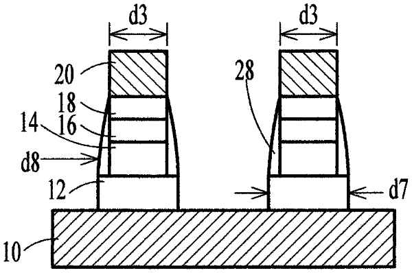
forming a stack of magnetic tunneling junction (MTJ) layers over a first electrode;
forming a second electrode on the stack of MTJ layers;
removing a first portion of the stack of MTJ layers to form a patterned first portion while using the first electrode as a mask, wherein a second portion of the stack of MTJ layers covers a top surface of the first electrode after the removing of the first portion of the stack of MTJ layers;
forming a spacer on a sidewall of the patterned first portion of the stack of MTJ layers; and
removing a first portion of the spacer to expose a sidewall surface of the second electrode.