| CPC H10N 30/875 (2023.02) [H10N 30/802 (2023.02); H10N 30/88 (2023.02); H03H 3/02 (2013.01); H03H 9/1021 (2013.01)] | 7 Claims |
|
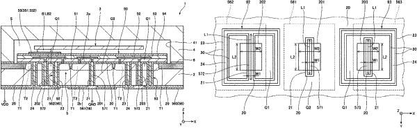
1. A vibration device comprising:
a semiconductor substrate having a first surface and a second surface in an obverse-reverse relationship;
an integrated circuit disposed on the first surface;
a first terminal which is disposed on the second surface and to which a substrate potential is applied;
a second terminal which is disposed on the second surface and to which a potential different from the substrate potential is applied;
a first through electrode which penetrates the semiconductor substrate, and is configured to electrically couple the first terminal and the integrated circuit to each other;
a second through electrode which penetrates the semiconductor substrate, and is configured to electrically couple the second terminal and the integrated circuit to each other;
a frame which penetrates the semiconductor substrate, and has an insulating property;
a vibration element disposed on the first surface; and
a lid bonded to the first surface, wherein
the first through electrode is located outside the frame, and
the second through electrode is located inside the frame.
|