| CPC H10N 30/2047 (2023.02) [B81B 2201/032 (2013.01); B81B 2203/0127 (2013.01)] | 20 Claims |
|
1. A MEMS optical device, comprising:
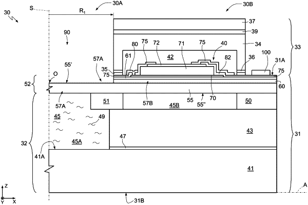
a substrate, the substrate housing a first cavity containing a fluid;
a deformable structure coupled to the substrate, the deformable structure includes:
a first portion and a second portion, the first portion of the deformable structure being suspended over the first cavity;
a first flexible layer covering the first cavity and including a first region and a second region, the first region being arranged adjacent to the first cavity, and the first region of the first flexible layer forms a first membrane; and
a second flexible layer over the second region of the first flexible layer, and the second region of the first flexible layer and the second flexible layer form a second membrane;
a piezoelectric actuator over the second portion of the deformable structure, the second region of the flexible layer being arranged adjacent to the piezoelectric actuator; and
a cap coupled to the second portion of the deformable structure and defining a chamber housing the piezoelectric actuator, and
wherein the substrate further includes a second cavity, the second cavity being arranged adjacent to the second region of the first flexible layer, and wherein the first membrane is suspended over the first cavity, and the second membrane is suspended over the second cavity.
|