US 11,818,937 B2
Organic light emitting display
Yo Han Kim, Seoul (KR); Yong Tack Kim, Yongin-si (KR); Yoon Hyeung Cho, Yongin-si (KR); Jong Jin Park, Cheonan-si (KR); Deok Chan Yoon, Hwaseong-si (KR); Yun Kyu Lee, Gumi-si (KR); and Dong Uk Choi, Sejong-si (KR)
Assigned to Samsung Display Co., Ltd., Yongin-si (KR)
Filed by Samsung Display Co., Ltd., Yongin-si (KR)
Filed on Dec. 6, 2021, as Appl. No. 17/543,483.
Application 17/543,483 is a continuation of application No. 16/706,559, filed on Dec. 6, 2019, granted, now 11,195,884.
Claims priority of application No. 10-2019-0014470 (KR), filed on Feb. 7, 2019.
Prior Publication US 2022/0093691 A1, Mar. 24, 2022
This patent is subject to a terminal disclaimer.
Int. Cl. H10K 59/38 (2023.01); H10K 50/13 (2023.01); H10K 50/115 (2023.01); H10K 50/844 (2023.01); H10K 50/84 (2023.01); H10K 59/12 (2023.01); H10K 59/35 (2023.01)
CPC H10K 59/38 (2023.02) [H10K 50/115 (2023.02); H10K 50/13 (2023.02); H10K 50/844 (2023.02); H10K 50/846 (2023.02); H10K 59/12 (2023.02); H10K 59/35 (2023.02)] 20 Claims
OG exemplary drawing
 
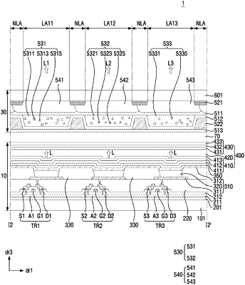
1. A display device comprising:
a first base substrate;
a plurality of light emitting diodes on the first base substrate;
a first inorganic layer on the plurality of light emitting diodes;
a second inorganic layer on the first inorganic layer and having a refractive index greater than a refractive index of the first inorganic layer;
an organic layer on the second inorganic layer;
a third inorganic layer on the organic layer; and
a plurality of wavelength conversion patterns on the third inorganic layer,
wherein a thickness of the first inorganic layer is 5000 Å or more, and
wherein the refractive index of the second inorganic layer is 1.5 to 1.57 for light having a wavelength of about 560 nm.