| CPC H10K 59/353 (2023.02) [G09G 3/3216 (2013.01); G09G 3/3225 (2013.01); H10K 59/131 (2023.02); H10K 59/179 (2023.02); H10K 59/351 (2023.02); H10K 59/352 (2023.02); G09G 2300/0426 (2013.01); G09G 2300/0452 (2013.01)] | 19 Claims |
|
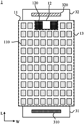
1. A display panel having a first display area and a second display area that are adjacent to each other; the display panel comprising:
a substrate;
a plurality of first light-emitting devices disposed on the substrate and located in the first display area;
a first driving circuit disposed on the substrate and coupled to the plurality of first light-emitting devices; wherein the first driving circuit is configured to actively drive the plurality of first light-emitting devices to emit light; the first driving circuit includes a plurality of pixel driving circuits and a signal line; the signal line is located in the second display area, and extends substantially along an edge of the second display area proximate to the first display area; and the signal line is coupled to pixel driving circuits located on two opposite sides of the second display area, and an orthographic projection of the signal line on the substrate and an orthogonal projection of the first display area on the substrate have a gap therebetween;
a plurality of second light-emitting devices disposed on the substrate and located in the second display area; and
a second driving circuit disposed on the substrate and coupled to the plurality of second light-emitting devices; wherein the second driving circuit is configured to passively drive the plurality of second light-emitting devices to emit light; wherein
an orthographic projection of at least one of the plurality of second light-emitting devices on the substrate is overlapped with an orthogonal projection of the gap on the substrate;
wherein the first driving circuit further includes scan signal lines configured to provide scan signals to the plurality of pixel driving circuits, and the scan signal lines extend along a first direction; the first direction is a direction along which the two opposite sides of the second display area are distributed.
|