| CPC H10K 59/1315 (2023.02) [H10K 59/126 (2023.02); H10K 59/1213 (2023.02); H10K 59/1216 (2023.02); H01L 27/1214 (2013.01); H10K 59/35 (2023.02); H10K 59/38 (2023.02)] | 20 Claims |
|
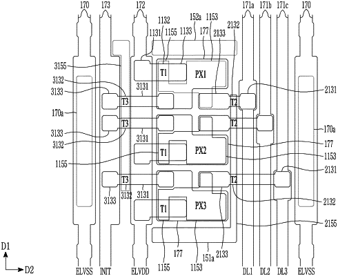
1. A display device comprising:
a substrate;
a first data line, a second data line, and a third data line extending in a first direction on the substrate and disposed to be adjacent to each other along a second direction crossing the first direction;
a semiconductor layer disposed on the first, second, and third data lines;
a first lower storage electrode, a second lower storage electrode, and a third lower storage electrode arranged to be adjacent along the first direction;
a first scan line extending in the second direction;
a first auxiliary scan pattern overlapping the first scan line and connected to the first scan line;
a first pixel connected to the first scan line and the first data line;
a second pixel connected to the first scan line and the second data line; and
a third pixel connected to the first scan line and the third data line,
wherein the first auxiliary scan pattern is disposed on a same layer as the first lower storage electrode and does not overlap the first, second, and third data lines.
|