US 11,818,925 B2
Light-emitting device, method for manufacturing the same, and cellular phone
Kaoru Hatano, Kanagawa (JP); Satoshi Seo, Kanagawa (JP); and Shunpei Yamazaki, Tokyo (JP)
Assigned to Semiconductor Energy Laboratory Co., Ltd., Atsugi (JP)
Filed by Semiconductor Energy Laboratory Co., Ltd., Atsugi (JP)
Filed on Dec. 27, 2021, as Appl. No. 17/562,085.
Application 16/930,373 is a division of application No. 15/276,071, filed on Sep. 26, 2016, granted, now 10,896,941, issued on Jan. 19, 2021.
Application 17/562,085 is a continuation of application No. 16/930,373, filed on Jul. 16, 2020, granted, now 11,289,558.
Application 15/276,071 is a continuation of application No. 14/103,990, filed on Dec. 12, 2013, granted, now 10,269,883, issued on Apr. 23, 2019.
Application 14/103,990 is a continuation of application No. 12/617,379, filed on Nov. 12, 2009, granted, now 8,610,155, issued on Dec. 17, 2013.
Claims priority of application No. 2008-294661 (JP), filed on Nov. 18, 2008.
Prior Publication US 2022/0123079 A1, Apr. 21, 2022
Int. Cl. H04M 1/02 (2006.01); H10K 59/127 (2023.01); H10K 50/84 (2023.01); H10K 59/122 (2023.01); H10K 59/124 (2023.01); H10K 71/50 (2023.01); H10K 77/10 (2023.01); H10K 59/12 (2023.01); H10K 102/00 (2023.01)
CPC H10K 59/127 (2023.02) [H04M 1/0269 (2022.02); H10K 50/841 (2023.02); H10K 50/846 (2023.02); H10K 59/122 (2023.02); H10K 59/124 (2023.02); H10K 59/1275 (2023.02); H10K 71/50 (2023.02); H10K 77/111 (2023.02); H10K 59/1201 (2023.02); H10K 2102/311 (2023.02); Y02E 10/549 (2013.01); Y02P 70/50 (2015.11)] 5 Claims
OG exemplary drawing
 
1. A display device comprising:
an EL panel comprising a light-emitting element over a flexible substrate;
a driver circuit overlapping with the EL panel;
a transistor over the flexible substrate;
a first insulating film over the transistor; and
an electrode of the light-emitting element over the first insulating film and electrically connected to the transistor,
wherein the EL panel is configured to display an image in a first direction and in a second direction different from the first direction,
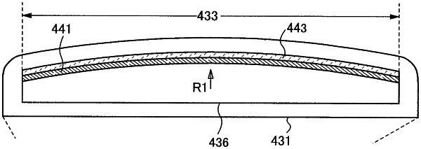
wherein the EL panel is bent in such a way that an edge of the EL panel overlaps with the EL panel with a curved region of the EL panel therebetween, and
wherein the driver circuit overlaps with the EL panel with the curved region provided therebetween.