| CPC H10K 59/124 (2023.02) [H01L 27/1225 (2013.01); H01L 27/1251 (2013.01); H01L 27/1255 (2013.01); H10K 59/1213 (2023.02); H10K 59/1216 (2023.02); H10K 71/00 (2023.02); H01L 25/167 (2013.01); H01L 25/18 (2013.01); H10K 59/1201 (2023.02); H10K 59/121 (2023.02); H10K 59/65 (2023.02)] | 8 Claims |
|
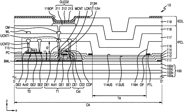
1. A display device comprising:
a substrate comprising a component area and a display area adjacent to the component area, the component area including a transmission area;
a first thin-film transistor comprising a first semiconductor layer arranged on the substrate and a first gate electrode overlapping the first semiconductor layer, the first semiconductor layer including a silicon semiconductor;
a first insulating layer covering the first gate electrode and overlapping the transmission area;
a second thin-film transistor comprising a second semiconductor layer arranged on the first insulating layer and a second gate electrode overlapping the second semiconductor layer, the second semiconductor layer including an oxide semiconductor;
a second insulating layer covering the second gate electrode and having a transmission hole overlapping the transmission area;
an intermediate insulating layer between the first insulating layer and the second insulating layer;
a conductive pattern between the intermediate insulating layer and the first insulating layer;
a display element arranged on the second insulating layer and spaced apart from the transmission area; and
a pattern layer arranged between the intermediate insulating layer and the second insulating layer and overlapping the component area,
wherein the transmission hole exposes an upper surface of the intermediate insulating layer, and
the pattern layer comprises an opening that entirely overlaps the transmission hole and exposes the upper surface of the intermediate insulating layer.
|