| CPC H10K 59/1213 (2023.02) [G09G 3/2003 (2013.01); G09G 3/3225 (2013.01); H10K 59/126 (2023.02); H10K 59/38 (2023.02); G09G 2360/145 (2013.01); H10K 59/131 (2023.02)] | 29 Claims |
|
1. A display device, comprising:
a display panel including a plurality of transistors and displaying an image on a front surface thereof; and
a sensing module on a rear surface of the display panel, wherein:
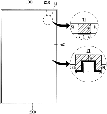
the display panel includes a first region that overlaps the sensing module and a second region that does not overlap the sensing module,
a W/L ratio of one of the transistors in the first region is greater than a W/L ratio of another of the transistors in the second region, the W/L ratio being obtained by dividing a width of a channel of the transistor by a length of the channel, and
the transistors in the second region each include a bent region between a source and a drain, and the transistors in the first region do not include a bent region, and
the number of transistors with bent regions is greater than the number of transistors with non-bent regions.
|