| CPC H10K 50/856 (2023.02) [H10K 50/858 (2023.02); H10K 59/122 (2023.02); H10K 71/00 (2023.02); H10K 59/1201 (2023.02)] | 11 Claims |
|
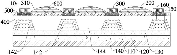
1. A display panel, comprising a display backboard,
wherein the display backboard comprises:
a base substrate, a thin film transistor array layer on a surface of the base substrate, a flattening layer on a side of the thin film transistor array layer away from the base substrate, and a pixel-defining layer on a surface of the flattening layer away from the base substrate,
wherein the pixel-defining layer comprises a first pixel-defining layer, the first pixel-defining layer defines a plurality of first openings, at least a portion of a sidewall of each first opening is provided with a reflective layer,
wherein the pixel-defining layer further comprises a second pixel-defining layer, the second pixel-defining layer is on exposed surfaces of the reflective layer and the first pixel-defining layer, and the second pixel-defining layer completely covers the exposed surfaces of the reflective layer and the first pixel-defining layer,
wherein the display panel further comprises:
a plurality of microlenses provided on a side of the first pixel-defining layer of the display backboard away from the base substrate, and surfaces of the plurality of microlenses away from the display backboard are a curved surface convex away from the display backboard, and an orthographic projection of at least one of the first openings on the base substrate at least partially overlaps with orthographic projections of the plurality of microlenses on the base substrate, and
a plurality of barriers provided on a side of the first pixel-defining layer away from the base substrate, adjacent ones of the barriers define a plurality of second openings, and the plurality of microlenses are provided in the plurality of second openings,
wherein a surface of the barriers is relatively hydrophobic relative to a surface of the display backboard away from the base substrate, and
wherein the display panel further comprises:
a packaging structure provided on the surface of the display backboard; and
a black matrix and a color resist layer, wherein the black matrix is disposed on a surface of the packaging structure away from the base substrate, the black matrix defines a plurality of third openings, the color resist layer is disposed in the plurality of third openings, and orthographic projections of the third openings on the base substrate at least partially overlap with orthographic projections of the first openings on the base substrate.
|