| CPC H10B 63/32 (2023.02) [H10N 70/231 (2023.02); H10N 70/826 (2023.02)] | 19 Claims |
|
1. A method, comprising:
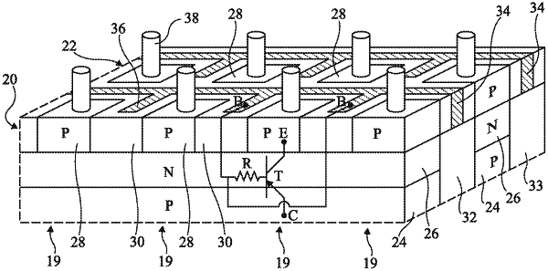
forming a row of bipolar transistors having a common base, the common base being located between a plurality of first conduction regions and a second conduction region, the first conduction regions separated from one another by insulator walls, an insulating trench being in contact with the row of bipolar transistors;
forming a cavity in the insulating trench and the insulator walls, side surfaces of the first conduction regions being exposed in the cavity;
forming a spacer layer in the cavity, the spacer layer covering the exposed side surfaces of the first conduction regions and a side surface of the insulating trench in the cavity; and
filling the cavity with a conductive material; and
forming a metal layer in the cavity and on the spacer layer prior to the filling the cavity with the conductive material.
|