| CPC H10B 63/24 (2023.02) [G11C 13/0004 (2013.01); H10B 61/10 (2023.02); H10B 63/84 (2023.02); H10N 50/01 (2023.02); H10N 50/80 (2023.02); H10N 70/063 (2023.02); H10N 70/231 (2023.02); H10N 70/24 (2023.02); H10N 70/25 (2023.02); H10N 70/8413 (2023.02); H10N 70/8825 (2023.02); H10N 70/8828 (2023.02); H10N 70/8833 (2023.02); H10N 70/8836 (2023.02)] | 15 Claims |
|
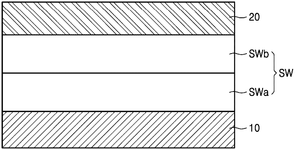
1. A semiconductor device comprising:
a first electrode;
a second electrode separated from the first electrode; and
a first chalcogen compound layer and a second chalcogen compound layer between the first electrode and the second electrode, wherein
the first chalcogen compound layer and the second chalcogen compound layer each independently include a first element selected from the group consisting of germanium (Ge) and tin (Sn) and a second element including one or more selected from the group consisting of sulfur (S), selenium (Se), and tellurium (Te), and
the first chalcogen compound layer and the second chalcogen compound layer have different compositions from each other,
wherein an energy band gap of the first chalcogen compound layer is greater than an energy band gap of the second chalcogen compound layer by an amount ranging from 0.1 eV to 1.0 eV.
|