| CPC H10B 43/35 (2023.02) [H10B 41/27 (2023.02); H10B 41/35 (2023.02); H10B 43/27 (2023.02)] | 10 Claims |
|
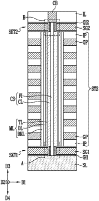
1. A semiconductor device comprising:
a stack structure including gate patterns and insulating patterns;
a channel layer penetrating the stack structure;
a source layer spaced apart from the stack structure;
a conductor spaced apart from the stack structure;
a first select transistor between the stack structure and the source layer; and
a second select transistor between the stack structure and the conductor,
wherein the first select transistor includes:
a first carbon layer in contact with the source layer and the channel layer;
a first select gate spaced apart from the first carbon layer; and
a first gate insulating layer between the first select gate and the first carbon layer, and
wherein the second select transistor includes:
a second carbon layer in contact with the conductor and the channel layer;
a second select gate spaced apart from the second carbon layer; and
a second gate insulating layer between the second select gate and the second carbon layer.
|