| CPC H10B 43/27 (2023.02) [G11C 5/063 (2013.01); G11C 16/0483 (2013.01); G11C 16/08 (2013.01); H10B 41/10 (2023.02); H10B 41/27 (2023.02); H10B 41/35 (2023.02); H10B 43/10 (2023.02); H10B 43/35 (2023.02); H01L 29/792 (2013.01)] | 12 Claims |
|
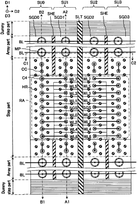
1. A semiconductor memory device comprising:
a plurality of first conductive layers stacked in a first direction and disposed between nearest of two first slits in a second direction;
a second conductive layer disposed above the plurality of first conductive layers and disposed between one of the nearest two first slits and a second slit;
a third conductive layer disposed above the plurality of first conductive layers and disposed between another of the nearest two first slits and the second slit;
a first pillar extending through the plurality of first conductive layers and the second conductive layer in the first direction, the first pillar including a semiconductor layer;
a second pillar extending through the plurality of first conductive layers and the third conductive layer in the first direction, the second pillar including a semiconductor layer;
a first plug extending in the first direction and in contact with the second conductive layer;
a second plug extending in the first direction and in contact with the third conductive layer;
a third plug extending through the plurality of first conductive layers and the second conductive layer in the first direction and electrically connected to the first plug; and
a fourth plug extending through the plurality of first conductive layers and the third conductive layer in the first direction and electrically connected to the second plug.
|