| CPC H10B 41/70 (2023.02) [G11C 16/045 (2013.01); G11C 16/10 (2013.01); G11C 16/14 (2013.01); G11C 16/26 (2013.01); H10B 41/35 (2023.02)] | 13 Claims |
|
1. An array structure of erasable programmable non-volatile memory cells, the array structures being constructed in a substrate, the array structure comprising:
an isolation structure formed on the substrate, wherein a surface of the substrate is divided into a first region and a second region by the isolation structure;
a first well region formed in the surface of the substrate corresponding to the first region;
a second well region formed in the surface of the substrate corresponding to the second region;
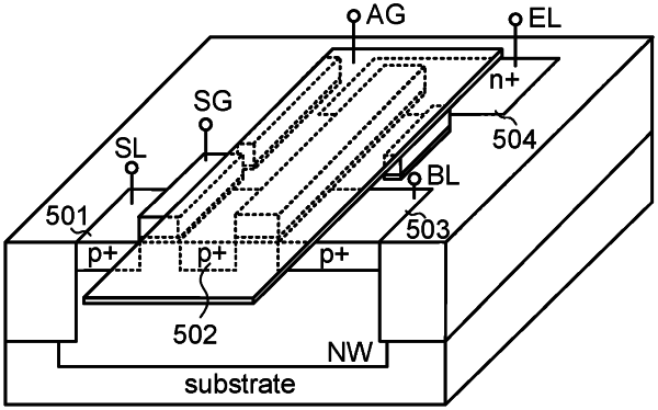
a first gate structure and a second gate structure formed on the surface of the first region, wherein the first region is divided into a first doped region, a second doped region and a third doped region by the first gate structure and the second gate structure, the first gate structure is connected to a first select gate line, the second gate structure is extended externally to the second region through a surface of the isolation structure, and a portion of the second region is covered by the second gate structure, the first doped region is connected to a source line, and the third doped region is connected to a first bit line;
a third gate structure formed on the isolation structure, and located beside a first side of the second gate structure;
a fourth doped region formed in the surface of the substrate corresponding to the second region, wherein the fourth doped region is connected to an erase line; and
a metal layer formed over the second gate structure, and electrically connected to the third gate structure, wherein the metal layer is connected to an assist gate line;
wherein the first gate structure comprises a first gate oxide layer and a first polysilicon gate layer, the second gate structure comprises a second gate oxide layer and a second polysilicon gate layer, and the third gate structure comprises a third gate oxide layer and a third polysilicon gate layer,
wherein the first doped region, the first gate structure and the second doped region are collaboratively formed as a first select transistor, the second doped region, the second gate structure and the third doped region are collaboratively formed as a first floating gate transistor, the second gate structure and the fourth doped region are collaboratively formed as a first MOS capacitor, the second polysilicon gate layer and the third polysilicon gate layer are collaboratively formed as a first poly/poly plate capacitor, and the second polysilicon gate layer and the metal layer are collaboratively formed as a first metal/poly plate capacitor,
wherein a first memory cell of the array structure comprises the first select transistor, the first floating gate transistor, the first MOS capacitor, the first poly/poly plate capacitor and the first metal/poly plate capacitor.
|