| CPC H10B 12/50 (2023.02) [G11C 11/4085 (2013.01); H01L 25/0652 (2013.01); H01L 29/4238 (2013.01); H01L 23/49816 (2013.01); H01L 23/49833 (2013.01); H01L 2225/06513 (2013.01); H01L 2225/06541 (2013.01)] | 20 Claims |
|
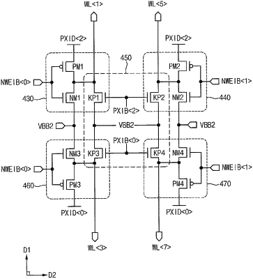
1. A semiconductor memory device comprising:
a first sub word-line driver including a first transistor configured to supply a negative voltage to a first word-line extending in a first direction in response to a driving signal; and
a second sub word-line driver including a second transistor configured to supply the negative voltage to a second word-line extending in the first direction in response to the driving signal,
wherein the first transistor and the second transistor comprise:
a first active pattern that extends in a second direction crossing the first direction and that is connected with the first word-line through a first direct contact;
a second active pattern that extends in the second direction, that is spaced apart from the first active pattern in the second direction by a first gap and that is connected with the second word-line through a second direct contact; and
a gate pattern on a portion of the first active pattern and a portion of the second active pattern, the gate pattern partially overlapping the first active pattern and the second active pattern,
wherein the first active pattern is connected with a third direct contact that does not overlap the gate pattern and that supplies the negative voltage, and
wherein the second active pattern is connected with a fourth direct contact that does not overlap the gate pattern and that supplies the negative voltage.
|