| CPC H10B 12/30 (2023.02) [H01L 28/60 (2013.01); H01L 29/7802 (2013.01)] | 20 Claims |
|
1. A method of fabricating a semiconductor device, the method comprising:
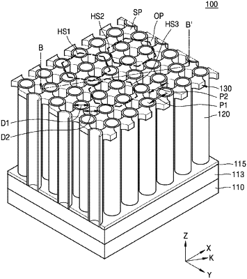
forming contact plugs on a semiconductor substrate;
forming a mold layer and a support forming layer on the contact plugs;
forming a plurality of open areas which expose the contact plugs, by etching the mold layer and the support forming layer;
forming a plurality of lower electrodes along internal walls of the plurality of open areas; and
forming a support which contacts the plurality of lower electrodes, by etching the support forming layer to define the plurality of open areas through an extreme ultraviolet (EUV) process of reflecting EUV light from an EUV photomask,
wherein a center point of each of the plurality of open areas is at a center point of a triangle formed by center points of three corresponding neighboring lower electrodes among the plurality of lower electrodes.
|