| CPC H10B 10/12 (2023.02) [H01L 21/823821 (2013.01); H01L 21/823842 (2013.01); H01L 21/823892 (2013.01); H01L 27/0924 (2013.01); H01L 27/0928 (2013.01); H01L 29/1083 (2013.01); H01L 29/4966 (2013.01)] | 9 Claims |
|
1. A method for manufacturing a semiconductor device, the method comprising:
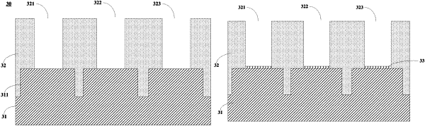
providing a substrate structure including a substrate, forming an interlayer dielectric layer on the substrate, forming a plurality of trenches in the interlayer dielectric layer exposing a surface of the substrate and comprising at least a first trench for forming a gate structure of a first transistor, a second trench for forming a gate structure of a second transistor, and a third trench for forming a gate structure of a third transistor;
performing a first doping into the substrate to form a first doped region in the substrate below a bottom of the first trench, the first doped region comprising an N-type dopant;
performing a second doping into the substrate to form a second doped region in the substrate below a bottom of the second trench, the second doped region comprising a first P-type dopant;
performing a third doping into the substrate to form a third doped region in the substrate below a bottom of the third trench, the third doped region comprising a second P-type dopant;
forming an interface layer on the bottom of the plurality of trenches;
forming a high-k dielectric layer on the interface layer and sidewalls of the plurality of trenches;
forming a first PMOS work function adjustment layer on the high-k dielectric layer of the third trench;
forming a second PMOS work function adjustment layer in the plurality of trenches after forming the first PMOS work function adjustment layer;
forming an NMOS work function adjustment layer in the plurality of trenches after forming the second PMOS work function adjustment layer; and
forming a barrier layer in the plurality of trenches after forming the NMOS work function adjustment layer, and forming a metal gate layer on the barrier layer.
|