| CPC H05K 3/28 (2013.01) [G06F 3/044 (2013.01); G06F 3/0412 (2013.01); G06F 3/0443 (2019.05); G06F 3/0445 (2019.05); G06F 3/0446 (2019.05); G02F 1/13338 (2013.01); G06F 2203/04103 (2013.01); H05K 1/11 (2013.01); H05K 2201/09381 (2013.01)] | 10 Claims |
|
1. A detection device comprising:
a substrate; and
a detection electrode on the first substrate,
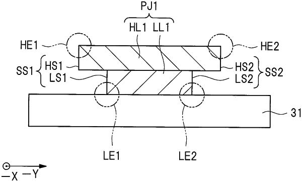
wherein the detection electrode has a lower layer portion and an upper layer portion which is on and in contact with the lower layer portion,
the lower layer portion being between the substrate and the upper layer portion,
both of the lower layer portion and the upper layer portion being conductive,
the upper layer portion has a first region which is in contact with the lower layer portion and overlaps the lower layer portion, and a second region which is not in contact with the lower layer portion and does not overlap the lower layer portion,
the first and second regions are located continuously,
a part of the detection electrode includes the lower layer portion and the upper layer portion, and
the detection electrode has a single layer portion consisting of a single layer and including an entirety of the detection electrode in a thickness direction of the detection electrode.
|
|
5. A substrate with a detection electrode comprising:
a base substrate; and
a lower layer portion and an upper layer portion which are included in the detection electrode,
wherein the lower layer portion on the base substrate and the upper layer portion which is on and in contact with the lower layer portion,
the lower layer portion being between the base substrate and the upper layer portion,
both of the lower layer portion and the upper layer portion being conductive,
the upper layer portion has a first region which is in contact with the lower layer portion and overlaps the lower layer portion, and a second region which is not in contact with the lower layer portion and does not overlap the lower layer portion,
the first and second regions are located continuously,
a part of the detection electrode includes the lower layer portion and the upper layer portion, and
the detection electrode has a single layer portion consisting of a single layer and including an entirety of the detection electrode in a thickness direction of the detection electrode.
|
|
9. A detection device comprising:
a substrate; and
a detection electrode on the first substrate,
wherein the detection electrode has a lower layer portion and an upper layer portion which is on and in contact with the lower layer portion,
the lower layer portion being between the substrate and the upper layer portion,
both of the lower layer portion and the upper layer portion being conductive,
the upper layer portion has a first region which is in contact with the lower layer portion and overlaps the lower layer portion, and a second region which is not in contact with the lower layer portion and does not overlap the lower layer portion,
the first and second regions are located continuously,
the second region protrudes from the first region, and
the detection electrode has a portion which does not have the second region, the portion being a part of the detection electrode and including an entirety of the detection electrode in a thickness direction of the detection electrode.
|