| CPC H05K 3/108 (2013.01) [H05K 3/064 (2013.01); H05K 3/423 (2013.01); H05K 2203/0143 (2013.01); H05K 2203/0554 (2013.01); H05K 2203/0582 (2013.01)] | 7 Claims |
|
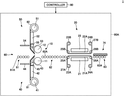
1. A resist layer forming method comprising:
laminating a resist layer on a base at a first pressure using a laminate roller having a first temperature;
pressing the resist layer against the base at a second pressure higher than the first pressure using a metal plate having a second temperature lower than the first temperature; and
roll-pressing the resist layer against the base at a third pressure, using a pressure roller having a third temperature, between the laminating the resist layer on the base and the pressing the resist layer against the base, wherein the second temperature is lower than each of the first temperature and the third temperature, and wherein the second pressure is higher than each of the first pressure and the third pressure.
|