| CPC H05K 1/112 (2013.01) [H05K 1/0222 (2013.01); H05K 1/115 (2013.01); H05K 1/025 (2013.01); H05K 1/0218 (2013.01); H05K 1/111 (2013.01)] | 21 Claims |
|
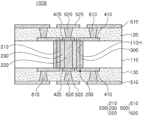
1. A printed circuit board, comprising:
a core layer;
a through portion penetrating through an upper surface and a lower surface of the core layer;
a first via disposed to be spaced apart from an inner surface of the through portion within the through portion;
a second via disposed inside the first via, and having a diameter, different from that of the first via;
an insulating material disposed between the first via and the inner surface of the through portion; and
a first via pad disposed on the first via,
wherein the first via pad is in contact with the core layer, the insulating material, and the first via.
|