| CPC H05K 1/111 (2013.01) [H05K 1/0218 (2013.01); H05K 3/34 (2013.01)] | 7 Claims |
|
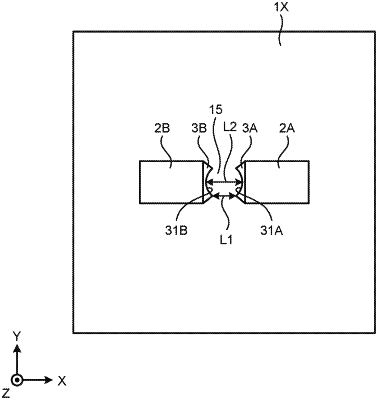
1. A printed wiring board comprising:
a first electrode pad to be soldered to a first electrode of an electronic component;
a second electrode pad to be soldered to a second electrode of the electronic component;
a first barrier conductor continuous with the first electrode pad; and
a second barrier conductor continuous with the second electrode pad, wherein
the first barrier conductor and the second barrier conductor are located at positions facing each other with an adhesive area therebetween, and the first electrode pad and the second electrode pad are positioned such that the first electrode pad faces the adhesive area with the first barrier conductor therebetween and that the second electrode pad faces the adhesive area with the second barrier conductor therebetween, the adhesive area being an area for an adhesive to be placed for adhesion of the electronic component, and
a longest distance between the first barrier conductor and the second barrier conductor in a direction of arrangement of the first electrode pad and the second electrode pad is equal to or longer than an inter-electrode distance, the inter-electrode distance being a distance between the first electrode and the second electrode.
|