| CPC H04N 25/772 (2023.01) [G01C 3/02 (2013.01); H01L 27/1461 (2013.01); H04N 25/63 (2023.01)] | 20 Claims |
|
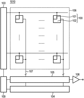
1. A photoelectric conversion device comprising:
at least one charge holding portion including a first semiconductor region of a first conductivity type formed under an electrode via an insulating layer and configured to hold signal charges based on incident light; and
an avalanche photodiode including a second semiconductor region of the first conductivity type and a third semiconductor region of a second conductivity type that is different from the first conductivity type,
wherein the signal charges are transferred from the first semiconductor region to the second semiconductor region via a fourth semiconductor region of the first conductivity type, and the third semiconductor region of the second conductivity type in this order, and
wherein the first semiconductor region is arranged above the fourth semiconductor region.
|