| CPC H04N 25/771 (2023.01) [H01L 27/14612 (2013.01); H01L 27/14656 (2013.01); H04N 25/57 (2023.01); H04N 25/589 (2023.01); H04N 25/59 (2023.01); H04N 25/767 (2023.01)] | 14 Claims |
|
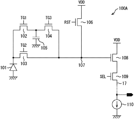
1. A light detecting device, comprising:
a photoelectric conversion region;
a first transmission transistor coupled to the photoelectric conversion region;
a second transmission transistor coupled to the photoelectric conversion region;
a first memory portion coupled to the first transmission transistor;
a second memory portion coupled to the second transmission transistor;
a third transmission transistor coupled to the first memory portion;
a fourth transmission transistor coupled to the second memory portion;
a floating diffusion coupled to the third transmission transistor and the fourth transmission transistor;
an amplification transistor coupled to the floating diffusion;
a selection transistor coupled to the amplification transistor;
a signal line coupled to the selection transistor;
a discharge transistor coupled between the photoelectric conversion region and a power source; and
circuitry is configured to:
read out a first signal corresponding to transmission of a first charge from the second memory portion to the amplification transistor, wherein
the fourth transmission transistor is configured to be turned on based on an end of an accumulation period,
the transmission of the first charge from the second memory portion to the amplification transistor is based on the turn on of the fourth transmission transistor, and
the third transmission transistor is configured to be turned on based on the read out of the first signal; and
read out a second signal corresponding to transmission of a second charge from the first memory portion to the amplification transistor, wherein
the transmission of the second charge from the first memory portion to the amplification transistor is based on the turn of the third transmission transistor.
|