| CPC H04N 25/75 (2023.01) [G01S 7/4808 (2013.01); G01S 17/26 (2020.01); G01S 17/89 (2013.01); H04N 23/80 (2023.01); H04N 25/40 (2023.01); H04N 25/745 (2023.01)] | 20 Claims |
|
1. An imaging device comprising:
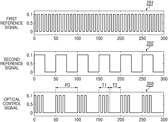
a light source configured to be operated by an optical control signal that is generated using a combination of a first reference signal having a first frequency and a second reference signal having a second frequency different from the first frequency for each frame period of a plurality of frame periods;
a plurality of pixels, each of the plurality of pixels including a photodiode configured to generate an electrical charge in response to a light reception signal output by the light source and reflected from a subject, and a pixel circuit configured to output a pixel signal corresponding to the electrical charge of the photodiode; and
a logic circuitry configured to generate raw data to generate a depth image using the pixel signal,
wherein the plurality of pixels includes first pixels and second pixels, and
the logic circuitry is configured to input a first photo control signal having the first frequency to the pixel circuit connected to the photodiode in each of the first pixels, and is configured to input a second photo control signal having the second frequency to the pixel circuit connected to the photodiode in each of the second pixels.
|