| CPC H04N 25/709 (2023.01) [H01L 27/14643 (2013.01); H01L 31/107 (2013.01)] | 12 Claims |
|
1. A photoelectric conversion device comprising:
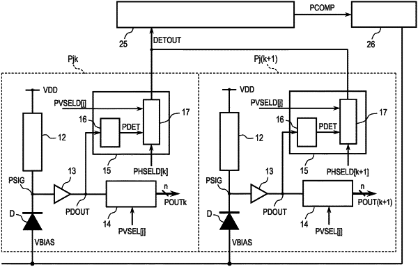
a plurality of pixels each including an avalanche diode that photoelectrically converts incident light and multiplies generated charge by an avalanche multiplication, a quench circuit that reduces the avalanche multiplication of the avalanche diode, a pulse conversion circuit that converts an output signal of the avalanche diode into pulses, and a signal generation circuit that generates an accumulation signal obtained by integrating or accumulating a number of pulses output from the pulse conversion circuit;
a detection circuit that detects whether or not the pulse output from the pulse conversion circuit has a width not smaller than a predetermined width; and
a voltage control circuit that controls a reverse bias voltage applied to the avalanche diode within a range not lower than a breakdown voltage of the avalanche diode based on a detection result of the detection circuit,
wherein the voltage control circuit includes an accumulation circuit that accumulates the number of pixels that output a pulse having a pulse width not smaller than the predetermined width and a signal comparison circuit that compares an accumulation value by the accumulation circuit with a predetermined value, and when the accumulation value is not less than the predetermined value, the reverse bias voltage applied to the avalanche diode is lowered within a range not lower than the breakdown voltage of the avalanche diode.
|