US 11,818,481 B2
Solid-state image sensor and electronic device
Tatsuki Nishino, Kanagawa (JP); Hiroki Hiyama, Kanagawa (JP); Shizunori Matsumoto, Kanagawa (JP); Takahiro Miura, Kanagawa (JP); Akihiko Miyanohara, Tokyo (JP); and Tomohiro Matsumoto, Kanagawa (JP)
Assigned to Sony Semiconductor Solutions Corporation, Kanagawa (JP)
Filed by Sony Semiconductor Solutions Corporation, Kanagawa (JP)
Filed on Nov. 15, 2022, as Appl. No. 17/987,266.
Application 17/987,266 is a continuation of application No. 16/649,808, granted, now 11,533,445, previously published as PCT/JP2018/031438, filed on Aug. 24, 2018.
Claims priority of application No. 2017-198122 (JP), filed on Oct. 12, 2017.
Prior Publication US 2023/0086897 A1, Mar. 23, 2023
This patent is subject to a terminal disclaimer.
Int. Cl. H04N 25/704 (2023.01); G01J 1/44 (2006.01); H01L 27/146 (2006.01); H04N 25/50 (2023.01)
CPC H04N 25/704 (2023.01) [G01J 1/44 (2013.01); H01L 27/14643 (2013.01); H04N 25/50 (2023.01); G01J 2001/4466 (2013.01)] 24 Claims
OG exemplary drawing
 
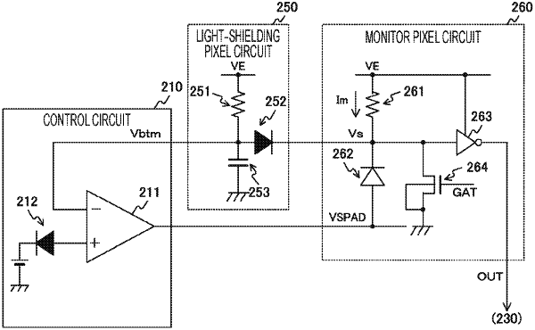
1. A light detecting device, comprising:
first pixel circuitry including a first avalanche photodiode and a first inverter, the first pixel circuitry configured to output a first output signal;
second pixel circuitry including a second avalanche photodiode and a second inverter, the second pixel circuitry configured to output a second output signal; and
control circuitry configured to receive the second output signal,
wherein an output of the control circuitry is coupled to an anode of the first avalanche photodiode and an anode of the second avalanche photodiode.